YILDIZ TECHNICAL UNIVERSITY
GRADUATE SCHOOL OF NATURAL AND APPLIED SCIENCES
PARTICLE SWARM OPTIMIZATION FOR ELECTRONIC
CIRCUIT DESIGN AUTOMATION
Revna ACAR VURAL, M.Sc in Electronics and Communication Engineering
Prepared within the framework of the Electronics Program at the Institute of Sciences Division of Electronics and Communication Engineering
PhD DISSERTATION
Date of Defence Examination : 11.02.2011
Supervisor : Prof. Dr. Tülay YILDIRIM (YTU) Members of the Examining Committee : Prof. Dr. Oğuzhan ÇİÇEKOĞLU (BU) :Prof. Dr. M. Oruç BİLGİÇ (KU) :Prof. Dr. Herman SEDEF (YTU) : Prof. Dr. Halit PASTACI (HU)
ii
Page
LIST OF SYMBOLS... iv
LIST OF ABBREVIATIONS ... v
LIST OF FIGURES ... vi
LIST OF TABLES ...viii
PREFACE... x
ABSTRACT ... xi
ÖZET ...xii
GENİŞLETİLMİŞ TÜRKÇE ÖZET...xiii
1. INTRODUCTION ... 1
2. EVOLUTIONARY ALGORITHMS AND ARTIFICIAL NEURAL NETWORKS .. 13
2.1 Evolutionary Algorithms ... 13
2.1.1 Particle Swarm Optimization... 15
2.1.2 Genetic Algorithm ... 17
2.1.3 Artificial Bee Colony Optimization ... 18
2.2 Artificial Neural Networks ... 19
2.2.1 Multilayer Perceptron ... 22
2.2.1.1 Backpropagation Training Algorithm ... 24
2.2.1.2 Levenberg-Marquardt Training Algorithm... 24
2.2.2 Radial Basis Functions ... 25
2.2.3 General Regression Neural Network ... 26
2.3 Particle Swarm Optimization- Artificial Neural Networks: A Hybrid Structure .. 27
2.3.1 Representation of Particle Vector ... 29
2.3.2 Evaluation (Fitness) Function... 29
2.3.3 The Processing Steps of PSO-ANN Hybrid Algorithm ... 30
2.3.4 PSO-MLP Application for Classification of Nonlinear Inputs: EXOR Problem .. 30
3. EVOLUTIONARY ALGORITHMS FOR DISCRETE CIRCUIT DESIGN ... 32
3.1 Analog Active Filter Structures ... 32
3.1.1 Butterworth Filter ... 33
3.1.2 State Variable Filter... 34
3.2 Conventional Design Method ... 35
3.3 Evolutionary Algorithm Based Active Filter Design ... 35
3.3.1 Butterworth Filter Design ... 36
iii
3.3.2.1 Component Representation for GA ... 38
3.3.2.2 Component Representation for PSO and ABC... 39
3.4 Simulation Results ... 40
3.4.1 Butterworth Filter Design Results ... 40
3.4.2 State Variable Filter Design Results... 44
3.5 Summary... 52
4. PARTICLE SWARM OPTIMIZATION FOR INTEGRATED CIRCUIT DESIGN.. 54
4.1 Particle Swarm Optimization for Digital Integrated Circuit Design ... 54
4.1.1 Dynamic Characteristics of an Inverter ... 54
4.1.2 PSO Based Inverter Design ... 58
4.1.2.1 Output Fall Time Estimation ... 58
4.1.2.2 Symmetric Output Response: Identical Fall and Rise Times ... 61
4.1.2.3 Symmetric Output Response & Identical Propagation Delay Times ... 63
4.1.3 Validation of PSO results with SPICE simulation ... 65
4.2 Particle Swarm Optimization for Analog Integrated Circuit Design... 67
4.2.1 Analog Integrated Circuit Structures ... 67
4.2.1.1 Differential Amplifier Structure ... 68
4.2.1.2 Two Stage Operational Amplifier Structure... 73
4.2.2 Design Procedure for Analog Integrated Circuits ... 74
4.2.2.1 Design Procedure for Differential Amplifier... 74
4.2.2.2 Design Procedure for Two-Stage Operational Amplifier... 75
4.2.3 Simulation Results of PSO Based Analog Integrated Circuit Design ... 76
4.2.3.1 Simulation Results of PSO based Differential Amplifier Design ... 76
4.2.3.2 Simulation Results of PSO based Two-Stage Operational Amplifier Design... 85
4.3 Summary... 91
5. ANN FOR TECHNOLOGY INDEPENDENT INTEGRATED CIRCUIT DESIGN. 94 5.1 Current Steering Type DAC Structure ... 94
5.2 Static Characterization of DAC ... 96
5.3 ANN Based Design Methodology ... 99
5.3.1 Measurement of SSP Values and Creation of DAC Database ... 100
5.3.2 Selection of Appropriate ANN Structure ... 103
5.3.3 GRNN Based Design Methodology ... 104
5.4 Simulation Results ... 106
5.5 Summary... 111
6. CONCLUSION... 113
REFERENCES ... 120
APPENDIXES... 129
Appendix 1 TSMC 0.25µm Technology Model Parameters ... 130
Appendix 2 TSMC 0.35µm Technology Model Parameters ... 133
Appendix 3 ON SEMI 0.5µm Technology Model Parameters ... 136
Appendix 4 ON SEMI 1.5 µm Technology Model Parameters ... 139
iv
c1,2 Acceleration factors
C Capacitor
Cox Oxide capacitance per unit area
CF Cost function
CP Crossover probability
di Desired value for ith output neuron
f -3dB Cut-off frequency
fj Activation function of jth hidden neuron
ft Unity-gain frequency
gbest Global best value
gm Transconductance of MOSFET
H Passband gain Ibias Bias current
L Gate length of MOSFET MP Mutation probability
N Number of particles
neti Net input to ith neuron
pbest Personal best value
Pdiss Power dissipation
Q Quality factor
R Resistor
SL Search limit
SN Maximum food number
Vtn Threshold voltage for NMOS
Vtp Threshold voltage for PMOS
VDS Drain-to-source voltage
VGS Gate-to-source voltage
vIC Common-mode input voltage
vID Differential-mode input voltage
VOS Input offset voltage
VDD Positive DC supply voltage
VSS Negative DC supply voltage
w Inertia weight parameter
wij Weight from neuron i to j
W Gate width of MOSFET
xpi Input i for pth data
φij Uniformly distributed real random number within the range [-1,1]
εp
p-dimensional vector of error
δ Local gradient σ Spread parameter
ω Angular frequency
τp Propagation delay time
µn,p Charge-carrier effective mobility
λ Channel-length modulation parameter
α Learning rate
v ABC Artificial Bee Colony
ACO Ant Colony Optimization ADC Analog/Digital Converter AIA Artificial Immune Algorithm ANN Artificial Neural Networks BP Backpropagation
BSIM Berkeley Short-channel IGFET Model CAD Computer Aided Design
CCII Second Generation Current Conveyor
CMOS Complementary Metal Oxide Semiconductor CMRR Common Mode Rejection Ratio
CSA Clonal Selection Algorithm DAC Digital/Analog Converter DNL Differential Nonlinearity DE Differential Evolution EA Evolutionary Algorithm EC Evolutionary Computation FET Field Effect Transistor
FPGA Field Programmable Gate Array GA Genetic Algorithm
GP Genetic Programming
GRNN General Regression Neural Networks IC Integrated Circuit
ICMR Input Common Mode Range INL Integral Nonlinearity
LNA Low Noise Amplifier LM Levenberg-Marquardt LSB Least Significant Bit MLP Multilayer Perceptron MOS Metal Oxide Semiconductor MSE Mean Square Error
NMOS N-channel Metal Oxide Semiconductor PE Processing Element
PSO Particle Swarm Optimization
PMOS P-channel Metal Oxide Semiconductor PSRR Power Supply Rejection Ratio
RBF Radial Basis Functions SA Simulated Annealing SI Swarm Intelligence
SPICE Simulation Program with Integrated Circuit Emphasis
SR Slew Rate
SSP Static Specification Parameters SVF State Variable Filter
TN Total Number of Initial Particles TS Tabu Search
TSMC Taiwan Semiconductor Manufacturing Company VCVS Voltage Controlled Voltage Source
vi
Page
Fig. 1.1 Optimization scheme for electronic circuit design (Massara, 1991) ... 2
Fig. 1.2 Pictorial comparison of classical and modern heuristic optimization strategies (Chan and Tiwari, 2007)... 4
Fig. 2.1 General EA procedures... 14
Fig. 2.2 Procedures of PSO algorithm ... 16
Fig. 2.3 Basic Computation Model of GA ... 17
Fig. 2.4 Procedures of ABC algorithm ... 18
Fig. 2.5 ANN Architecture (Haykin, 1999) ... 19
Fig. 2.6 Common nonlinear activation functions-Soft nonlinearity (a) Sigmoid and (b) Hyperbolic Tangent;- Hard nonlinearity (c) Signum and (d) Step... 20
Fig. 2.7 Neural Computation [1]... 21
Fig. 2.8 General Procedures of an Artificial Neural Network ... 21
Fig. 2.9 MLP Structure ... 22
Fig. 2.10 RBF Structure ... 25
Fig. 2.11 GRNN Architecture (Specht, 1991a)... 26
Fig. 2.12 Particle vector representing weight values ... 29
Fig. 3.1 Butterworth 4th order VCVS low-pass filter (Jiang et al., 2007) ... 33
Fig. 3.2 State variable 2nd order low-pass filter (Schaumann and Valkenburg, 2001) ... 34
Fig. 3.3 Component values in a chromosome for Butterworth filter ... 37
Fig. 3.4 Component values in a chromosome for SVF... 39
Fig. 3.5 Box and whisker plots for Butterworth filter design with E12 series over 20 runs42 Fig. 3.6 CF values vs. iteration number for GA method (E12 series) ... 42
Fig. 3.7 CF values vs. iteration number for ABC method (E12 series) ... 42
Fig. 3.8 CF values vs. iteration number for PSO method (E12 series)... 43
Fig. 3.9 Frequency responses of conventional and EA based design of Butterworth filter (E12)... 44
Fig. 3.10 Box and whisker plots for SVF design with E24 series over 20 runs ... 47
Fig. 3.11 Box and whisker plots for SVF design with E96 series over 20 runs ... 47
Fig. 3.12 CF values vs. iteration number for GA method (E24 series) ... 48
Fig. 3.13 CF values vs. iteration number for ABC method (E24 series) ... 48
Fig. 3.14 CF values vs. iteration number for PSO method (E24 series)... 49
Fig. 3.15 CF values vs. iteration number for GA method (E96 series) ... 49
Fig. 3.16 CF values vs. iteration number for ABC method (E96 series) ... 49
Fig. 3.17 CF values vs. iteration number for PSO method (E96 series)... 50
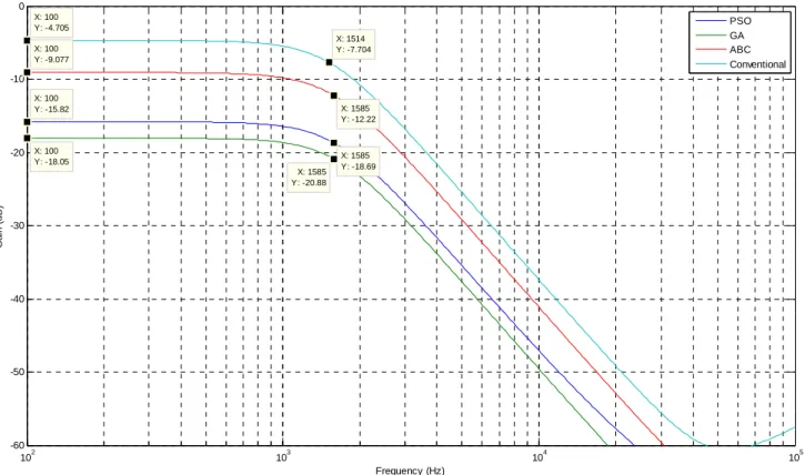
Fig. 3.18 Frequency responses of conventional and EA based design of SVF filter (E24).. 51
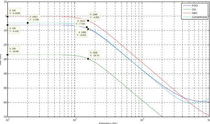
Fig. 3.19 Frequency responses of conventional and EA based design of SVF filter (E96).. 52
Fig. 4.1 Inverter Structure ... 54
Fig. 4.2 (a)Load capacitance discharges through NMOS transistor (b) Output voltage waveform during high-to-low transition (Kang and Leblebici, 2005) ... 55
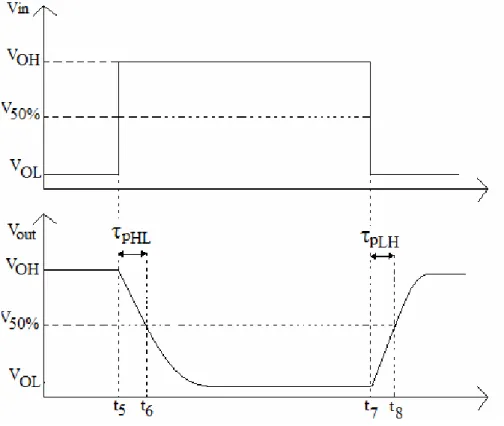
Fig. 4.3 (a)Load capacitance charges through PMOS transistor (b) Output voltage waveform during low-to-high transition (Kang and Leblebici, 2005) ... 56
Fig. 4.4 Input and output voltage waveforms of a typical inverter and definitions of propagation delay times (DeMassa and Ciccone, 1996) ... 57
Fig. 4.5 CF value vs. iteration number for the 5th design ranges for Case Study-I... 60
Fig. 4.6 CF value vs. iteration number for the first design in case study-II... 63
vii
vID and common mode, vIC, input voltages (Allen and Holberg, 2002)... 68
Fig. 4.10 Small signal model for the CMOS differential amplifier (a) Exact model... 70
(b) Simplified equivalent model. ... 70
Fig. 4.11 Configurations for simulating design specifications for (a) Gain and Phase Margin (b) Offset voltage (c) CMRR (d) ICMR (e) PSRR (f) Output voltage swing ... 72
Fig. 4.12 Two-stage Operational Amplifier (Allen and Holberg, 2002) ... 73
Fig. 4.13 PSO Based Differential Amplifier with Current Mirror Load Design Results-I... 78
Fig. 4.14 PSO Based Differential Amplifier with Current Mirror Load Design Results-II . 80 Fig. 4.15 Frequency response of PSO based Differential Amplifier with Current Mirror Load ... 81
Fig. 4.16 Phase margin of PSO based Differential Amplifier with Current Mirror Load .... 81
Fig. 4.17 Offset voltage of PSO based Differential Amplifier with Current Mirror Load ... 82
Fig. 4.18 Slew rate of PSO based Differential Amplifier with Current Mirror Load ... 82
Fig. 4.19 ICMR-Vic(min) of PSO based Differential Amplifier with Current Mirror Load 82 Fig. 4.20 ICMR-Vic(max) of PSO based Differential Amplifier with Current Mirror Load. 83 Fig. 4.21 PSRR- of PSO based Differential Amplifier with Current Mirror Load ... 83
Fig. 4.22 PSRR+ of PSO based Differential Amplifier with Current Mirror Load... 83
Fig. 4.23 PSO Based Two-stage Operational Amplifier Design Results... 86
Fig. 4.24 Frequency response of PSO based Two-stage Operational Amplifier ... 87
Fig. 4.25 Phase margin of PSO based Two-stage Operational Amplifier ... 88
Fig. 4.26 Output voltage range of PSO based Two-stage Operational Amplifier ... 88
Fig. 4.27 Slew rate of PSO based Two-stage Operational Amplifier ... 88
Fig. 4.28 ICMR -Vic(min) of PSO based Two-stage Operational Amplifier ... 89
Fig .4.29 ICMR - Vic(max) of PSO based Two-stage Operational Amplifier... 89
Fig. 4.30 PSRR- of PSO based Two-stage Operational Amplifier ... 89
Fig. 4.31 PSRR+ of PSO based Two-stage Operational Amplifier... 90
Fig. 5.1 Current steering 4-bit CMOS DAC circuitry (Hoeschele, 1994) ... 95
Fig. 5.2 DNL and INL errors for 3-bit DAC... 97
Fig. 5.3. Gain error for 3-bit DAC ... 98
Fig. 5.4. Illustration of nonmonotonic transition for 3-bit DAC... 98
Fig. 5.5 General Technology Independent Design Methodology for DAC... 99
Fig. 5.6 Transient response of DAC design with ON SEMI 1.5 µm (Serin, 2008) ... 100
Fig. 5.7 DAC Database Structure... 103
Fig. 5.8 Validation of Test Results with GRNN Based Design Methodology ... 105
Fig. 5.9. Test error of GRNN Based Design Methodology for proper samples ... 107
Fig. 5.10 Improvement of monotonicity for 57th test sample by GRNN Based Methodology... 109
Fig. 5.11 DNL Improvement of GRNN based methodology (b) over actual output (a) for 57th test sample ... 109
Fig. 5.12 INL Improvement of GRNN based methodology (b) over actual output (a) for 57th test sample ... 110
viii
Page Table 1.1 The error rate and synthesis time of various analog CAD tools
(Lee and Kim, 2006)... 6
Table 2.1 Truth table for XOR... 30
Table 2.2 Training Performance of PSO-MLP Structure ... 31
Table 3.1 Effects of Genetic Algorithm’s Own Parameters on Butterworth Filter Performance ... 41
Table 3.2 Effects of PSO Algorithm’s Own Parameters on Butterworth Filter Performance... 41
Table 3.3 Effects of ABC Algorithm’s Own Parameters on Butterworth Filter Performance... 41
Table 3.4 Previous Methods and GA, ABC, PSO Techniques for Butterworth Filter Design ... 43
Table 3.5 Effects of Genetic Algorithm’s Own Parameters on SVF Performance (E24) ... 45
Table 3.6 Effects of Genetic Algorithm’s Own Parameters on SVF Performance (E96) ... 45
Table 3.7 Effects of PSO Algorithm’s Own Parameters on SVF Performance (E24) ... 46
Table 3.8 Effects of PSO Algorithm’s Own Parameters on SVF Performance (E96) ... 46
Table 3.9 Effects of ABC Algorithm’s Own Parameters on SVF Performance (E24) ... 46
Table 3.10 Effects of ABC Algorithm’s Own Parameters on SVF Performance (E96) ... 47
Table 3.11 Previous Methods and GA, ABC, PSO Techniques for SVF Design ... 50
Table 4.1 PSO inputs and outputs for Case Study-I ... 59
Table 4.2 Specified Ranges and PSO Synthesized Results for Case Study-I... 59
Table 4.3 Evolution of Particles for 5th design of Case Study-I ... 60
Table 4.4 PSO Inputs and Outputs for Case Study-II... 61
Table 4.5 Specified Ranges and PSO Synthesized Results for Case Study-II ... 62
Table 4.6 Evolution of Particles for first design of Case Study-II ... 62
Table 4.7 Specified Ranges and PSO Synthesized Results for Case Study-III ... 64
Table 4.8 Initial and Final Positions of Particles for 5th design of Case Study-III ... 65
Table 4.9 SPICE Results vs. PSO Results for Case-I... 66
Table 4.10 SPICE Results vs. PSO Results for Case-II... 66
Table 4.11 SPICE Results vs. PSO Results for Case-III ... 66
Table 4.12 Inputs and Outputs for PSO based Differential Amplifier Design ... 77
Table 4.13 Comparison of classical method and PSO based method by means of design specifications ... 79
Table 4.14 Comparison of classical method and PSO based method by means of design parameters ... 79
Table 4.15 Comparison of DARWIN and PSO with bias current improvement by means of design specs... 84
Table 4.16 Comparison of DARWIN and PSO with bias current improvement by means of design parameters... 84
Table 4.17 PSO Inputs and Outputs for PSO based Two-stage Operational Amplifier... 85
Table 4.18 Comparison of Convex Optimization and PSO based design method by means of design specifications ... 90
Table 4.19 Comparison of Convex Optimization and PSO based design method by ... means of design parameters... 91
Table 5.1 PMOS width and length values for DAC design with ON SEMI 1.5 µm technology... 100
ix
Table 5.4 INL error values for each digital input word ... 101
Table 5.5 PMOS width and length values for DAC design with ON SEMI 0.5 µm technology... 102
Table 5.6 PMOS width and length values for DAC design with TSMC 0.35 µm technology... 102
Table 5.7 Training error values depending to PSO-MLP parameters ... 104
Table 5.8 Performance of GRNN based design methodology for test sample–1 ... 106
Table 5.9 DNL and INL results of GRNN based method for whole test set ... 107
x
This dissertation was written during my time as a doctoral candidate at the Department of Electronics and Communication Engineering, Yildiz Technical University. Throughout my doctoral studies, I was supported by several people and Scientific Research Coordination Department, Yildiz Technical University. At this point, I should express my sincere thanks. First and foremost, I would like to thank my supervisor Prof. Dr. Tulay Yildirim for her guidance and support from the very beginning of my academic studies. It has been over eight years since she has been supervising me, facilitating my research projects and academic development. Her constant support and encouragement kept me going at times where the burden of a PhD seemed unbearable. I also would like to thank Prof. Dr. Oguzhan Cicekoglu and Prof. Dr. Oruc Bilgic for their valuable advices and instructions during my doctoral research. I owe special thanks to my dear friends and colleagues Asst. Prof. Dr. Burcu Erkmen, Asst. Prof. Dr. Nihan Kahraman and Dr. Tuba Kiyan for their support and encouragement. Furthermore, I would like to thank to Scientific Research Coordination Department, Yildiz Technical University for sponsoring the ongoing academic research project with project number: 29-04-03-KAP01.
I would like to express my deepest gratitude to my beloved family; my dearest husband Cem Vural, our precious son Berk Vural, my brother Arda Acar and my parents Ayse Rezzan Acar and Yilmaz Acar. During my doctoral studies, they encouraged me with great patience and understanding. Without their love and everlasting support, I could have never succeeded. I also would like to thank to my best friends Yasemin Engin, Ozge Saracoglu and Cagla Yilmaz who individually have always been a true sister for me.
Finally, I dedicated this thesis to my beloved grandfather Mehmet Nezihi Onen who passed away during my final months in PhD. He was very willing to witness my graduation and always had faith in my decisions. I always counted on his support and endless compassion.
xi
PARTICLE SWARM OPTIMIZATION FOR ELECTRONIC CIRCUIT DESIGN AUTOMATION
Together with the increase in electronic circuit complexity, the design and optimization processes have to be automated with high accuracy. Predicting and improving the design quality in terms of performance, robustness and cost is the central concern of electronic design automation. Generally, optimization is a very difficult and time consuming task including many conflicting criteria and a wide range of design parameters. The evolutionary algorithms were introduced as an efficient method for exploring the search space and handling multi objective optimization problems. Therefore, fast and accurate evolutionary methods are being utilized for accommodating required functionalities and performance specifications in electronic circuit design automation area.
Particle swarm optimization (PSO) is an evolutionary algorithm technique based on the social behavior, movement and intelligence of swarms searching for an optimal location in a multidimensional search area. In this dissertation, the applicability of PSO as a global optimization tool has been investigated comprehensively for electronic circuit design automation. For this purpose, PSO was utilized for fast and optimal design of discrete and integrated circuit design having a fixed topology for a particular process technology. However, due to the rapid evolution of process technologies, the expectation for changing process technologies need to be accounted in the design cycle. Therefore, technology independent circuit design methodologies need to be developed. Considering discrete circuits, performance of PSO has been investigated, whether optimized design error will be affected in case different manufactured series are utilized for selection of components of a particular filter topology. Following, a more difficult analog design problem is considered and PSO is used in a hybrid configuration. Performance of the hybrid method is compared with different approaches for technology independent design of a digital to analog converter.
Simulation results indicate that as a global optimization tool, PSO is a very efficient method for optimal component selection and sizing task in electronic circuit design automation by means of both high accuracy and short computation time. Since once programmed, no human intervention is required (e.g. to provide an initial “good design” or to interactively guide the optimization process), the proposed method yields completely automated sizing of optimal circuits by means of both discrete and integrated design concepts.
Keywords: Particle Swarm Optimization, Artificial Neural Networks, Multi-objective Optimization, Design Automation.
xii
ELEKTRONİK DEVRE TASARIM OTOMASYONU İÇİN PARÇACIK SÜRÜ
OPTİMİZASYONU
Elektronik devre karmaşıklığı arttıkça, tasarım ve optimizasyon süreçlerinin yüksek doğrulukla otomatikleştirilmesi gerekmektedir. Elektronik devre tasarım otomasyonunun merkezindeki konu, tasarım kalitesinin performans, güvenilirlik ve maliyet açısından kestirimi ve iyileştirilmesidir. Genel olarak optimizasyon, çok sayıda birbiriyle çelişen kriter ve çeşitli tasarım parametrelerini içeren zor ve çok zaman alıcı bir süreçtir. Evrimsel algoritmalar, arama uzayını araştırabilecek ve çok amaçlı optimizasyon problemlerinin üstesinden gelebilecek etkili bir yöntem olarak önerilmiştir. Bu sebeple hızlı ve doğru evrimsel metotlar, elektronik devre tasarım otomasyonu alanında gerekli fonksiyonelliği ve performans tanımlamalarını sağlamak üzere kullanılmaktadır.
Parçacık Sürü Optimizasyonu (PSO), çok boyutlu arama uzayındaki en iyi konumu araştıran sürülerin sosyal davranış, hareket ve zekasını temel alan evrimsel bir algoritmadır. Bu tezde, küresel bir optimizasyon aracı olan PSO’nun elektronik devre tasarım otomasyonuna uygunluğu kapsamlı olarak incelenmiştir. Bu amaçla PSO, belirli bir üretim teknolojisi için sabit bir topolojiye sahip ayrık ve entegre devrelerin hızlı ve optimum tasarımında kullanılmıştır. Bununla birlikte üretim teknolojilerinde hızlı gelişmeye bağlı olarak, üretim teknolojilerinin gelişeceği beklentisi de tasarım sürecine dahil edilmelidir. Bundan dolayı, teknolojiden bağımsız devre tasarım yöntemleri geliştirilmelidir. Ayrık devreler dikkate alındığında PSO’nun performansı, belirli bir filtre topolojisinin eleman seçiminde farklı üretim serileri kullanıldığı durumda, optimize edilmiş devrenin tasarım hatasının etkilenip etkilenmediğine bağlı olarak incelenmiştir. Ardından daha karmaşık bir analog tasarım problemi ele alınmış ve PSO karma bir düzenleme içerisinde kullanılmıştır. Karma düzenlemenin performansı, sayısal analog çevirici devresinin teknolojiden bağımsız tasarımı için farklı yaklaşımlarla karşılaştırılmıştır.
Simülasyon sonuçları, elektronik devre tasarım otomasyonunda optimum eleman seçimi ve boyutlandırma işi için küresel bir optimizasyon aracı olan PSO’nun etkili bir yöntem olduğunu göstermektedir. Bir kez programlandıktan sonra kullanıcı müdahalesi gerekmediğinden (iyi bir başlangıç noktası bulmak, optimizasyon sürecini yönlendirmek vs...) önerilen yöntem, hem ayrık hem de entegre tasarım açısından devrelerin tamamen otomatik olarak boyutlandırmasını sağlamaktadır.
Anahtar Kelimeler: Parçacık Sürü Optimizasyon, Yapay Sinir Ağları, Çok amaçlı Optimizasyon, Tasarım Otomasyonu.
xiii
Devre tasarım süreci entegre devrenin içindeki tek bir transistörden karmaşık elektronik sistemlere kadar geniş bir aralığı kapsamaktadır. Tasarım, devrenin çalışma prensiplerinin tanımlanması ile başlar. Bu tanımlamalar, devrenin yapısı karmaşıklaştıkça daha fazla tasarım parametresi içerecek; bununla birlikte tanımlamalar da birbiriyle çelişir hale gelecektir. Arama uzayı büyüdükçe kullanıcının optimum tasarıma ulaşmak için bu süreci otomatikleştirecek bir takım araçlar kullanması gerekmektedir. Günümüzdeki karmaşık devre yapıları göz önüne alındığında, devre topolojisinin belirlenmesi, uygun değer boyutlandırma ve serim optimizasyonu için tasarım araçlarının kullanılması kaçınılmazdır. Elektronik devre tasarım otomasyonu için kullanılan bu araçların yüksek doğrulukla çalışması ve hızlı işlem yapabilmesi büyük önem taşımaktadır.
Belirli bir devre topolojisi için optimum boyutlandırma işlemi çok amaçlı optimizasyon problemi olarak tanımlanabilir. Çok sayıda tasarım parametresi içeren çelişkili tanımlamaları ve tasarım kısıtlamalarını sağlayan optimum tasarım parametrelerini elde etmek için çeşitli optimizasyon yöntemleri önerilmiştir. Klasik ve buluşsal teknikler, algoritmalarda kullanılan değişkenlere, arama uzayının boyutuna ve dışbükeylik durumuna bağımlı olduğu için özellikle optimum boyutlandırma gibi çok amaçlı optimizasyon problemleri için yetersiz kalmaktadır. Kendi kendine organize olan sistemlerin birbirleri ve çevreleri ile etkileşimini inceleyen sürü zekası temelli sistemler bahsedilen bu eksikleri gidermek üzere önerilmiştir. Parçacık Sürü Optimizasyonu (PSO), çok boyutlu arama uzayındaki en iyi konumu araştıran sürülerin sosyal davranış, hareket ve zekasını temel alan evrimsel bir algoritmadır. Bu tezde, küresel bir optimizasyon aracı olan PSO’nun elektronik devre tasarım otomasyonuna uygunluğu kapsamlı olarak incelenmiştir. Bu amaçla PSO, belirli bir üretim teknolojisi için sabit bir topolojiye sahip ayrık ve entegre devrelerin hızlı ve optimum tasarımında kullanılmıştır. Tasarım kriterleri programa tanıtılarak belirlenen sınırlar içerisinde devrenin boyutlandırma işleminin PSO algoritması tarafından yapılması hedeflenmiştir. Bununla birlikte üretim teknolojilerinde hızlı gelişmeye bağlı olarak, üretim teknolojilerinin gelişeceği beklentisi de tasarım sürecine dahil edilmelidir. Ayrık devreler açısından farklı üretim serileri ve entegre devreler açısından farklı üretim teknolojileri kullanılarak aynı devre tasarımının minimum hata kriteri ile gerçeklenmesi hedeflenmiştir. PSO algoritması ile birlikte incelenen diğer yöntemler Bölüm 2’de verilmiştir.
Ayrık devre tasarımı çerçevesinde analog aktif filtrelerin pasif eleman değerlerinin üretim serilerine uygun olarak seçilmesi, bu devrelerin kullanılabilirliği açısından çok önemlidir. Filtre tasarımında kullanılan geleneksel yönteme göre, elemanlar ideal kabul edilir ve tasarım sırasında sınırsız değer alabilir. Halbuki kapasite ve direnç gibi ayrık elemanlar sabit ve tercih edilen değerlere göre üretilirler. Filtre tasarımında eleman değerleri, tasarımda kullanılan formüle ve tasarım kriterlerine (kesim frekansı, kalite faktörü) bağlı olarak hesaplanır. Bu hesaplamayı kolaylaştırmak için birbirine eşit seçilen bazı ayrık eleman değerlerine bağlı olarak elde edilen diğer ayrık eleman değerleri, tercih edilen değerlerle örtüşmeyebilir. Devrenin performansı, seçilen en yakın tercih edilen değerlere bağlı olarak düşebilir ve bu durum devre için belirlenen hata kriteri değerinin artmasına sebep olur. Optimize edilmiş bir tasarım gerçekleştirmek için tercih edilen değerlerin tüm olası kombinasyonları üzerine bir arama yapmak geçerli bir çözüm değildir. Örneğin, sekiz elemanlı devre yapısı göz önüne alındığında, eleman değerleri E12 üretim serisinden dört dekat aralığında seçilecekse, arama uzayı 3x10¹³ nokta içerir ki; mantıklı bir süre içerisinde bilgisayar destekli arama yapılıp bu noktaların değerlendirilmesi pek mümkün değildir. Bölüm 3’te incelenen bu problemde evrimsel algoritmalar, iki farklı filtre yapısının minimum hata ile tasarımı için farklı üretim
xiv
düşük tasarım hatası gözetilerek seçimi bakımından incelenmiştir. Durum değişkenli filtre yapısında ise evrimsel algoritmaların seçtiği pasif elemanlarla yapılan tasarım sonucunda elde edilen toplam hata değerinin farklı bir üretim serisi kullanılması durumunda önemli ölçüde etkilenmemesi hedeflenmektedir.
Entegre devreler sayısal ve analog olarak ikiye ayrılmaktadır. Anahtarlama karakteristiği, sayısal entegre devrelerin hızını belirleyen önemli bir etkendir. Bu nedenle tasarım aşamasının başında optimize edilmesi gereklidir. Analog entegre devrelerdeki tasarım problemi ise çok sayıda çelişkili tasarım kriterine ve tasarım kısıtlamalarına uygun en küçük MOSFET alanını elde etmektir. Günümüzde yaygın olarak kullanılan sayısal tasarım araçları olmasına rağmen analog entegre devre otomasyonu halen geliştirilme aşamasındadır. Sayısal entegre tasarımında başarıyla kullanılan genel amaçlı kütüphane tabanlı yaklaşım, uygulamaya çok bağlı olan analog yaklaşımda pek geçerli olmamaktadır. Literatürde önerilen çeşitli analog entegre devre tasarım araçları, MOSFET boyutlandırma problemi için çeşitli optimizasyon yöntemlerinden faydalanmaktadır. Bu yöntemler simülasyon veya denklem tabanlıdır. Simülasyon tabanlı yaklaşımlar oldukça uzun sürmekte, denklem tabanlı olanlar da bir önceki yaklaşım kadar yüksek doğruluğa ulaşamamaktır. Dolayısıyla yüksek doğruluklu ve hızlı optimizasyon yöntemlerine ihtiyaç duyulmaktadır. Bölüm 4’te PSO algoritması hem sayısal hem analog entegre devre tasarım problemlerine uygulanmıştır. Sayısal bir devre olan CMOS eviricinin anahtarlama karakteristiğini optimize edecek CMOS boyutları PSO yardımıyla 3 farklı senaryo için elde edilmiştir. Bununla birlikte, denklem tabanlı bir yöntem olarak, PSO analog entegre devre tasarımında kullanılmış, elde edilen sonuçlar SPICE simülasyonu ve literatürde önerilen yöntemler ile karşılaştırılmıştır. Bu amaçla, farksal kuvvetlendirici ve işlemsel kuvvetlendirici yapıları incelenmiş, birbiriyle çelişen tasarım kriterlerini ve tasarım kısıtlamalarını sağlayacak optimum MOSFET boyutları PSO yardımıyla belirlenmiştir. Burada tasarım problemini PSO’ya tanıtabilmek için tasarım kriterlerini ve MOS yapıların kanal genişliklerinin (W), kanal boylarına (L) oranlarını değişken olarak içeren bir denklem oluşturulmalıdır. PSO’nun bulması gereken, bu denklemin minimum noktası ve bu minimum noktayı sağlayan tasarım kriter değerleri ve W/L oranlarıdır.
Bununla beraber, devredeki transistör sayısı arttığı zaman sadece devre denklemleriyle tasarım yapmak mümkün olmamaktadır. Karmaşık devre yapıları için, tasarımda karşılaşılan bütün idealsizliklerin ve lineer olmayan durumların temsil edilebildiği hızlı ve yüksek doğruluklu çözümler önerilmelidir. Ayrıca, üretim teknolojilerinde hızlı gelişmeye bağlı olarak, üretim teknolojilerinin gelişeceği beklentisi de tasarım sürecine dahil edilmeli ve teknolojiden bağımsız devre tasarım yöntemleri geliştirilmelidir. Çok karmaşık, uzun ya da çok sayıda düzensiz bilgi taşıyan böylesi verilerin çözümlenebilmesinde, devre tanımlama denklemlerine ihtiyaç duymadan, simülasyon sonuçları ile oluşturulan veri kümesinin giriş ve çıkışlarını haritalayabilen yapay sinir ağları (YSA) yaygın olarak kullanılmaktadır. Ağa tanıtılan örnekler için doğru çıkışları üretecek, diğer bir deyişle ağ çıkışı ile hedef çıkış arasındaki hatayı en aza indirgeyecek ağırlık değerlerinin bulunması çok boyutlu optimizasyon problemidir. Bu işlemler ağ yapısına bağlı olarak tek adımda veya yinelemeli olarak gerçekleştirilebilir ve hedeflenen hata değerine ulaşıldığı durumda ağın “öğrendiği” kabul edilir. Yinelemeli işlemlerde kullanılacak olan optimizasyon algoritması, özellikle veri kümesinin büyük boyutlu olduğu durumda, problemin niteliğine uygun olarak seçilmelidir. Bölüm 5’te farklı ağ yapılarının performansı sayısal analog çeviricinin teknoloji parametrelerinden bağımsız tasarımı için incelenmiştir. İlk olarak problemi temsil edecek veri kümesi oluşturulmuştur. Daha sonra çok büyük boyutlu bu problemin çözümünde hem tek
xv incelenmiştir.
Bu tezde PSO algoritmasının elektronik devre tasarımında kullanılabilirliği farklı özellikte ve farklı boyutta tasarım problemleri açısından incelenmiştir. Türev hesabı gerektirmemesi ve ayarlanacak parametre sayısının az olması algoritmayı hızlandırırken, parçacıkların birbirleriyle ve çevreleriyle etkileşim prensibi arama uzayının etkili olarak araştırılmasına ve dolayısıyla küresel optimum noktanın keşfedilmesini sağlamaktadır. Simülasyon sonuçları ve diğer yöntemlerle yapılan karşılaştırmalar, elektronik devre tasarım otomasyonunda optimum eleman seçimi ve boyutlandırma işi için küresel bir optimizasyon aracı olan PSO’nun etkili bir yöntem olduğunu göstermektedir. Bir kez programlandıktan sonra kullanıcı müdahalesi gerekmediğinden önerilen yöntem, hem ayrık hem de entegre tasarım açısından devrelerin tamamen otomatik olarak boyutlandırmasını sağlamaktadır.
1. INTRODUCTION
The process of circuit design can cover systems ranging from complex electronic systems all the way down to the individual transistors within an integrated circuit and begins with the specification, which states the functionality that the finished design must provide, but does not indicate how it is to be achieved (Sherwani, 1999).The initial specification is basically a technically detailed description of what the customer wants the finished circuit to achieve and can include a variety of electrical requirements, such as what signals the circuit will receive, what signals it must output, what power supplies are available and how much power it is permitted to consume. The specification can also set some of the physical parameters that the design must meet, such as size, weight, moisture resistance, temperature range, thermal output, vibration tolerance and acceleration tolerance. Given a set of design specifications, a designer first initiates the circuit design by determining a circuit topology. It is most frequently the case that the designer modifies a known topology rather than creates a completely new one. The designer usually selects from well-characterized topologies or previously adopted ones, or builds one by combining them. Decision criteria rely on rough performance estimations of circuits. Next, the designer determines the values of designable parameters of a selected topology, such as transistor sizes and component values, to satisfy given specifications. Early in this stage, the designer may use analytical equations that express the relations between circuit performance and design parameters, and assign approximate values to the design parameters. Later these values are refined according to accurate performance evaluations performed by a circuit simulator such as SPICE.
Several types of parameters p=(x,s) influence the dynamic and static behavior of electronic circuits and have to be taken into account when optimizing appropriate performance functions
f(p): design parameters x and manufacturing process parameters s. During optimization,
performance function f(p) should be minimized while also several constraints have to be satisfied. The performance function f(p) and the constraint functions c(p) can be costly to evaluate and are subject to noise (i.e. due to numerical integration effects). For both, the dependency on p can be highly nonlinear (Maten et al., 2006). Once the specialized constraints of particular circuit design problem have been properly formulated as an optimization problem, the techniques that then are utilized are totally unspecialized in character. Optimization thus provides a truly general design engineering scheme (Fig.1.1) and extensively used in following electronic design areas (Massara, 1991):
• Design accommodating complex device models
• Design accommodating non-standard specification constraints (minimum component
spread, minimum sensitivity to component variations, maximum yield, etc.)
• Large-scale analog and digital circuit design; printed circuit board and interconnection;
integrated circuit design and layout (e.g., minimum interconnection length, optimum placement of major functional blocks)
• Distributed device design (microwave, surface acoustic waveform structures, etc.) • Passive component and topology selection in analog and digital filter design • Neural network training for applications in electronic engineering
Fig. 1.1 Optimization scheme for electronic circuit design (Massara, 1991)
Integrated circuits (IC) are characterized by complex tradeoffs between multiple nonlinear objectives while satisfying multiple nonlinear and sometimes non convex constraints. Typical of IC objective and/or constraint functions are area, delay, and power. Expressed as functions of the usual IC designable parameters, such as stripe widths and supply voltages, these objectives are frequently, and, in physical limits, inherently, in competition with one another.
As an example wideband amplifier designmay have performance functions as the noise figure and the bandwidth of the amplifier and specifications may be set that the input and output impedances are within 5 percent of 50 Ω over the band of the amplifier. Here, there exists two criteria to be evaluated and these are clearly conflicting. Moreover the specifications over the input and output impedances have to be satisfied for all frequencies in the band of the amplifier. Thus IC design problem with conflicting criteria can be characterized as constrained multi objective optimization problem. (Brayton et al., 1981)
Together with the increase in circuit complexity, the design and optimization complexity of today’s ICs has increased drastically. Obtaining the optimal solution for a particular combination of design criteria by hand is unaffordable and time consuming. Selection of independent design parameters is quite important in design process. Ideally all design parameters are accepted as variables and the optimal solution is searched. However, tremendous growth of search space makes the search process inefficient. In addition; there are several relations that should hold between certain L, W, and W/L ratios to make the search space smooth and the optimization process reliable. Therefore efficient optimization methods for automation of optimal sizing of MOS transistors are required. Classical approaches are either deterministic or statistical-based techniques. Deterministic methods, such as Simplex (Nelder & Mead, 1965), Branch and Bound (Land and Doig, 1960), Goal Programming (Scniederjans, 1995), Dynamic Programming (Bellman, 2003) are effective only for small size problems. They are not efficient when dealing with multi-criteria problems. In addition, it has been proven that these optimization techniques impose several limitations due to their inherent solution mechanisms and their tight dependence on the algorithm parameters. Besides they rely on the type of objective, the type of constraint functions, the number of variables and the size and the structure of the solution space. Moreover they do not offer general solution strategies. Most of the optimization problems require different types of variables, objective and constraint functions simultaneously in their formulation. Statistical methods generally start with finding a “good” DC quiescent point, which is provided by the skilled analogue designer. Following, a simulation-based tuning procedure takes place. However these statistic-based approaches are time consuming and do not guarantee the convergence towards the global optimum solution (Talbi, 2002). Therefore, classic optimization procedures are generally not adequate. Heuristics are necessary to solve big size problems and/or with many criteria (Basseur et al., 2006). They can be ‘easily’ modified and adapted to suit specific problem requirements. Even though they don’t guarantee to find in an exact way the optimal solution(s), they give ‘good’ approximation of it (them) within an
acceptable computing time (Chan and Tiwari, 2007). Some mathematical heuristics that were previously utilized were Local Search (Aarts and Lenstra, 2003), Simulated Annealing (SA) (Kirkpatrick et al., 1983; Siarry et al., 1997), Tabu Search (TS) (Glover, 1989; Glover, 1990), Genetic Algorithms (GA) (Grimbleby, 2000; Dreo et al., 2006), etc.
Fig. 1.2 Pictorial comparison of classical and modern heuristic optimization strategies (Chan and Tiwari, 2007)
However these techniques do not offer general solution strategies that can be applied to problem formulations where different types of variables, objectives and constraint functions are used. In addition, their efficiency is also highly dependent on the algorithm parameters, the dimension of the solution space, the convexity of the solution space, and the number of variables. Actually, most of the circuit design optimization problems simultaneously require different types of variables, objective and constraint functions in their formulation. Hence, the abovementioned optimization procedures are generally not adequate or not flexible enough. In order to overcome these drawbacks, a new set of nature inspired heuristic optimization algorithms were proposed. The thought process behind these algorithms is inspired from the collective behavior of decentralized, self-organized systems. It is known as Swarm Intelligence (SI) (Bonabeau et al. 1999). SI systems are typically made up of a population of simple agents interacting locally with each other and with their environment. These particles obey to very simple rules, and although there is no centralized control structure dictating how each particle should behave, local interactions between them lead to the emergence of
complex global behavior. Most famous such SIs are Ant Colony Optimization (ACO) (Dorigo et al., 1999), Artificial Bee Colony optimization (ABC) (Karaboga, 2005) and Particle Swarm Optimization (PSO) (Kennedy and Eberhart, 1995; Clerc, 2006). PSO, in its current form, has been in existence for almost a decade, which is a relatively short period when compared to some of the well known natural computing paradigms, such as evolutionary computation. PSO has gained widespread demand amongst researchers and has been shown to offer good performance in an assortment of application domains (Banks et al., 2007).
Above mentioned optimization methods are incorporated into computer-aided design tools (CAD) for optimal sizing of complex ICs together with topology selection (Maulik et al., 1992) and actual circuit layout (Harvey et al., 1992). CAD tools are the key to managing this increased complexity while meeting the shortening time-to-market factor. Predicting and improving the design quality in terms of performance, robustness and cost is a central concern of computer aided circuit design. CAD tools are also needed to assist or automate many of routing and repetitive design tasks, taking away the tedium of manually designing these sections and providing the designer with more time to focus on the creative aspects of the design (Gielen and Rutenbar, 2000).
The analog design medium has proven to be a formidable domain to its digital counterpart for many high performance IC applications. In digital domain, CAD tools are fairly well developed and commercially available today, certainly for lower level of the design flow. While digital synthesis tools have evolved in phase with digital revolution, analog portion of design automation has not been able to keep up with its demand. Some of the main reasons for this lack of automation are that analog design in general is perceived as less systematic and more heuristic and knowledge-intensive in nature than digital design. The variety of circuit schematics and number of conflicting requirements and corresponding diversity of device sizes are also much larger. These differences from digital design explain why analog CAD tools cannot simply adapt digital algorithms but why specific analog solutions need to be developed that are targeted to the analog design paradigm and complexity. Historically, researchers developed two mainstreams of analog automation methodologies. One of the early approaches uses optimization-based method which optimizes a set of performance constraints characterized by complicated trade-offs and makes extensive use of detailed circuit simulator embedded in the inner loop of optimization engine. This mechanism works quite well for tuning purpose of the circuit that is already close to a good design. These techniques require many iterations to adjust transistor sizes and optimization engine needs to evaluate
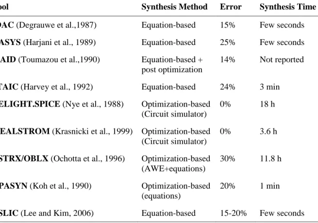
corresponding performance at each cycle. This procedure is very time consuming and computationally expensive task. Second approach is equation-based method which is based on inverse process of circuit analysis technique. Since sizing of a circuit is done mathematically, the automation is much faster while accuracy is not as good as the first approach due to the simplified device equations and approximations. Comparison of previously proposed analog CAD tools is given in Table 1.1 (Gielen and Rutenbar, 2000; Lee and Kim, 2006).
Table 1.1 The error rate and synthesis time of various analog CAD tools (Lee and Kim, 2006)
Tool Synthesis Method Error Synthesis Time
IDAC (Degrauwe et al.,1987) Equation-based 15% Few seconds OASYS (Harjani et al., 1989) Equation-based 25% Few seconds ISAID (Toumazou et al.,1990) Equation-based +
post optimization
14% Not reported
STAIC (Harvey et al., 1992) Equation-based 24% 3 min DELIGHT.SPICE (Nye et al., 1988) Optimization-based
(Circuit simulator)
0% 18 h
MEALSTROM (Krasnicki et al., 1999) Optimization-based (Circuit simulator)
0% 3.6 h
ASTRX/OBLX (Ochotta et al., 1996) Optimization-based (AWE+equations)
30% 11.8 h
OPASYN (Koh et al., 1990) Optimization-based (equations)
20% 1 min
ASLIC (Lee and Kim, 2006) Equation-based 15-20% Few seconds
Among the CAD tools tabulated above, STAIC, DELIGHT.SPICE, and OPASYN utilize classical optimization techniques while IDAC, MAELSTROM, ASTRX/OBLX, ASLIC, and OASYS are heuristic based systems. Kruiskamp and Leenaerts (1995) developed a GA based CMOS operational amplifier synthesis tool (DARWIN) for topology selection and circuit sizing. Massier et al. (2008) proposed sizing rules method for CMOS and bipolar analog IC synthesis. Sripramong and Toumazou (2002) introduced an automated circuit design system for the evolution and subsequent invention of CMOS amplifiers. This system utilized genetic programming for evolving new circuit topologies and current-flow analysis for screening and correcting circuits. Hershenson et al. (2001) proved that the design of CMOS op-amp can be
well approximated as polynomial convex optimization problem that can then be solved using geometric programming techniques, producing a close-by-first-cut design in an extremely efficient way. In (Liu et al., 2009), an evolution-based methodology named memetic single-objective evolutionary algorithm is developed for automated sizing of high-performance analog IC circuits. Guerra-Gomez et al. (2009) proposed multi-objective evolutionary algorithm based on decomposition (MOEA/D) for optimization of second generation current conveyors (CCII). Mentioned system uses HSPICE as circuit evaluator. Considering optimal CCII design without any circuit evaluator; a multi-objective heuristic (Salem et al.,2006; Fakhfakh et al., 2009a) and PSO algorithm (Cooren et al., 2007; Fakhfakh et al., 2009b; Fakhfakh et al., 2010) are utilized by formulating the requirements for the design of CCII in terms of boundaries on performance functions. Tawdross and König (2005) investigated PSO as an alternative to GA genetic algorithm for field programmable analog scalable device array reconfiguration. For this purpose an operational amplifier with particular design constraints was designed using PSO taking into different external influences such as high temperature and fabrication faults. Having successful results authors extended their PSO based dynamic hardware design environment to functional block level (Tawdross and König, 2006). A 3-bit ADC structure is developed using previously designed op-amps and resistors. Thakker et al. (2009) extended PSO algorithm to a hierarchical scheme for automatic sizing of low power analog circuits where simulation of circuits is performed with Cadence Spectre. Microwave circuit design is another area where optimization tools were widely used. Considering less computation time, PSO was chosen as the synthesis procedure for two sets of microwave circuits: micro stripe coupler and single shunt stub matching circuit (Ulker, 2008). Tulunay and Balkir (2008) proposed an automatic synthesis tool of a cascade low noise amplifier (LNA). Fakhfakh et al. (2010) utilized PSO technique for optimal sizing of CMOS LNA with inductive degeneration design. Choi and Allstod (2006) developed a SA algorithm based synthesis tool that includes an adaptive tunneling mechanism and post-optimization sensitivity analysis with respect to design, process and temperature variations. A very detailed investigation about the state of the art in applying EAs for the synthesis and sizing of analog ICs was presented by Tlelo-Cuautle et al. (2010).
Considering digital ICs, circuit delays often need to be reduced to obtain faster response times, with a minimal area penalty. A typical digital IC consists of multiple stages of combinational logic blocks that lie between latches, clocked by system clock signals. Delay reduction must ensure that the worst-case delay of the combinational blocks is such that valid signals reach a latch before any transition in the signal clocking the latch, with allowances for
set-up time requirements. In other words, the worst-case delay of each combinational stage must be restricted to be below a certain specification. Given the MOS circuit topology, the delay can be controlled by varying the sizes of transistors in the circuit. Here, the size of a transistor is measured in terms of its channel width, since the channel lengths in a digital circuit are generally uniform. Roughly speaking, the sizes of certain transistors can be increased to reduce the circuit delay at the expense of additional chip area (Sapatnekar, 1993). As an optimization tool, PSO was utilized in field programmable gate arrays (FPGA) placement and routing for minimization of the distances between configurable logic blocks (Gudise and Venayagamoorthy, 2004). Venayagamoorthy et al. (2007) proposed PSO algorithm as a method for determining the parameters for circuit partitioning problem and this method optimized the critical path as well as the number of partitioning and test vectors. Gate level design of combinational logic circuits is another area where PSO was successfully utilized for minimizing the number of gates during realization of 100% feasible circuits (Coello Coello, 2003; Moo Moore and Venayagamoorthy, 2005; Moore and Venayagamoorthy, 2006). Vural et al. (2010c) utilized PSO for inverter design having symmetric output response. Having obtained successful results authors enhanced their work to a more detailed dynamic characterization of inverter design framework considering three different case studies (Vural et al., 2010d).
So far it has been mentioned about optimization in analog and digital IC design. Despite the extensive usage of ICs, discrete components are still preferred in analog active filter design. Conventionally, the values of passive components used in the active filters are chosen as equal to each other. This approach simplifies the design procedure but also limits the freedom of design. Moreover, components are assumed to be ideal and have infinite value during analog design process. However, discrete components such as resistors and capacitors are produced in approximate logarithmic multiples of a defined number of constant values such as E12 series. There are also E24, E48, E96 and E192 ranges for components of tighter tolerance with 24, 48, 96 and 192 different values within each decade, respectively. In order to reduce the costs and make the design more reliable, discrete components are chosen from these industrial series or other possible produced preferred values. Performing an exhaustive search on all possible combinations of preferred values for obtaining an optimized design is not feasible when components are selected from the tighter tolerance series over wide decade range. Therefore, intelligent search methods must be developed that requires short computation time with high accuracy.
The application of evolutionary techniques in filter design automation and optimization is a promising area which is based on concepts of natural selection and survival of the fittest. In (Wang et al., 2005), optimal microwave filter design with arbitrary geometries is aimed to be designed with particle swarm optimization (PSO) and finite element method. Coefficient optimization of digital filters with numerous evolutionary approaches was investigated in (Karaboga, 2009; Luitel and Venayagamoorthy, 2008). In (Zebulum et al., 1998), a detailed comparative study on analog passive filter design with different evolutionary methodologies was presented. An automated passive analog circuit synthesis procedure based on GA was utilized for the simultaneous generation of both the topology and the component value selection in (Das and Vemuri, 2007). Component value and topology evolution were also studied in (Koza et al., 1997) by means of genetic programming (GP) and in (Chang et al., 2006) by using GP based tree representation method. Unconstrained and constrained evolutions were applied towards design of analog LCR low pass filter (Sapargaliyev and Kalganova, 2006). This work has been a successful attempt to application of evolutionary strategy method for analog filter design. A robust design paradigm that exploits the open-ended topological synthesis capability of GP was developed in (Hu et al., 2005) to evolve robust low-pass and high-pass analog passive filters. In (Goh and Li, 2001), a GA based growing technique for component value optimization of analog passive filters was presented. Component value selections of analog passive and active filters were also investigated in (Sheta, 2010). Sheta (2010) explored the advantages of differential evolution (DE) over numerical optimization approaches to perform the operation of selecting the best values of circuit elements for various types of band-pass filters. In (Zebulum et al., 1999; Xu and Ding, 2009) component value selection and topology optimization of analog active filter has been performed using GA and adaptive immune GA, respectively. Moreover, some particular analog active filter types were also optimized using evolutionary approaches in the literature. A voltage controlled voltage source (VCVS) low pass Butterworth active filter circuit was designed using clonal selection algorithm (CSA) and results of CSA based design were compared with results of tabu search (TS) based, GA based, and conventional design methods (Jiang et al., 2007). In (Vural and Yildirim, 2010a), a PSO based component value selection method has been utilized for the optimal design of the same circuit topology used in (Jiang et al., 2007) and less design error was obtained when compared with results of (Jiang et al., 2007). In (Horrocks and Spittle, 1993; Kalinli, 2004; Kalinli, 2006), component values of a low pass state variable active filter (SVF) circuit was selected using GA, TS and artificial immune algorithm (AIA), respectively. However, (Horrocks and Spittle, 1993; Kalinli, 2004;
Kalinli, 2006) used a different calculation of cutoff frequency than regular and practical expression of cutoff frequency statement used in (Vural and Yildirim, 2010b).
Abovementioned electronic circuit design problems were all considered for a particular technology. However, the ability to accurately predict the performance of circuits made of MOSFETs or high-speed VLSI interconnects barely keeps pace with the technology that shrinks the FET and printed circuit board dimensions, increases the operating speed, and creates new devices. The arising problem is that as their dimensions are reduced or a new device is developed, the old device or circuit models are no longer suitable. Consequently, new models have to be developed in order to use and predict the performances of the new device or circuit. This, however, is not valid for neural networks which not only being computationally very efficient but also are flexible and general. Therefore, there is a growing interest in applying the potential of neural networks to many new fields especially in CAD of VLSI circuits.
In ANN modeling of VLSI circuits, complex semiconductor equations are not required and the parameter extraction step, which represents a difficult and time consuming method, can also be omitted. Some researchers have tried to predict the transistors’ sizes for basic integrated circuits where the circuit outputs are used as inputs for ANN (Wolfe and Vemuri, 2003; Jianjun et al., 2003; Pratap, 2005; Zhongliang, 2004). However, technology independent neural network modeling for VLSI design automation has not been explored until (Kahraman, 2008). Kahraman (2008) proposed a method to predict the transistor sizes of fundamental circuits that correspond to design constraints, with minimum user effort and design knowledge for a newer design technology, using neural networks. In contrast to other modeling researches, the output specifications of integrated circuits are predicted for new technology designs. A huge database was constituted using AC and DC simulations of basic analog and digital circuits varying transistor sizes with Cadence Spectre Analog Environment. This database was applied to different ANN architectures so as to estimate the transistor sizes of the circuit that meet the design constraints in new technology successfully. While predicting the new transistor sizes, ANN does not need any technology parameters. ANN just learns from the database that was constituted before, calibrates its synaptic weights, calculates an error function and predicts the output for new data (Kahraman, 2008; Kahraman and Yildirim, 2008a, 2008b). Selection of the appropriate ANN architecture for high dimensional electronic circuit design database is very important. First of all, selected structure should be able to process input information with a massive feature. Method of training should be
considered as well, since error backpropagation method would require a very long time for training high-dimensional database due to the derivation procedures. Furthermore a multi-layer perceptron (MLP) trained by error backpropagation, the most commonly used ANN, requires that the analyst determine the appropriate number of hidden layer nodes, the initial connection weights, and the form of the activation function (Currit, 2002). Recently PSO algorithm was proposed as an alternative training method for MLP. Performances of the mentioned training algorithms were compared with PSO and more accurate results were obtained with PSO in shorter computation time (Mendes et al., 2002; Zhao et al., 2005; Kuo, 2007; Junyou, 2007; Al-Kazemi and Mohan, 2002; Braendler and Hendtlass, 2002; Zhang et al., 2000). The aim is to minimize classification and generalization error (Zhao et al., 2005), mean absolute percentage error (Junyou, 2007) and/or mean square error (Junyou, 2007; Kuo, 2007; Mendes et al., 2002; Zhao et al., 2005; Al-Kazemi and Mohan, 2002; Zhang et al., 2000). Besides software applications PSO is also applied to training of a neural hardware. The challenge of training a neural hardware is to store the bit values representing weight and bias values; increasing bit values enhances the accuracy as well as the hardware complexity. Braendler and Hendtlass (2002) reported that limited number of bits utilized by PSO for weight quantization did not affect accuracy significantly and fast execution capability of PSO is very advantageous on training neural hardware. Vural and Yildirim (2008) proposed a method for ANN based optimization of ICs by utilizing PSO as a training algorithm for MLP. This dissertation has two objectives: The first one is to explore evolutionary algorithms, particularly Particle Swarm Optimization algorithm on electronic circuit design automation. PSO-based method is applied to both discrete and integrated circuit design problems with particular technology parameters. The problem considered in this dissertation is the selection of component values and transistor dimensions, which is only a part of a complete analog circuit CAD tool. Other parts which are beyond the scope of this work are the topology selection (Maulik et al., 1992) and actual circuit layout (Harvey et al., 1992). The optimal component selection and transistor sizing of the CAD process remains between these two tasks. As reported in the literature, simulation-based optimization technique requires very long execution time and equation-based methods are less accurate than the former method. Therefore, optimization methods with high accuracy and short computation time are necessary for design automation. PSO as a global optimization method has fewer primitive mathematical operators than in GA (e.g reproduction, mutation and crossover) and those mathematical operations require more fine-tuning of own parameters which leads to longer computation time. Second objective of this dissertation is to investigate and compare ANN
methods including a PSO-trained one for a more complex circuit design problem; technology independent digital-to-analog converter (DAC) design automation.
The organization of this dissertation is as follows: Section 2 provides an insight of the evolutionary techniques utilized for both discrete and integrated circuit design cases and artificial neural network structures utilized for technology independent design of a selected DAC structure.Discrete circuit design with evolutionary algorithms is investigated in Section 3. Here, passive components of two different analog active filter structures are selected using EAs for two different manufactured series. Results are discussed in detail. Section 4 describes the PSO-based method for integrated circuit design. For this purpose, design equations of both differential amplifier with current mirror load source and two-stage operational amplifier are derived and equation-based PSO method is utilized for optimal sizing of MOS transistors for minimum occupied area. Section 5 is dedicated to technology independent neural network modeling of CMOS current-steering type DAC. Here, all ANN structures described in Section 2 are utilized for this very high-dimensional dataset and performance of the each structure is evaluated. Section 6 concludes with a discussion of simulation results and suggests possible extensions.
2. EVOLUTIONARY ALGORITHMS AND ARTIFICIAL NEURAL NETWORKS In this section, Particle Swarm Optimization (PSO), Genetic Algorithm (GA) and Artificial Bee Colony optimization (ABC) algorithm as evolutionary algorithms and Multilayer Perceptron (MLP), Radial Basis Function neural network (RBF) and General Regression Neural Network (GRNN) as artificial neural network structures utilized for electronic circuit design were investigated. Among evolutionary algorithms, PSO algorithm is the main concern of this thesis and is explained more detailed since its performance results reported in the literature is very promising and it has not been widely used for electronic circuit design area. PSO is also used as a training algorithm for MLP in order to investigate whether it can enhance MLP performance for very high dimensional electronic circuit design database when used instead of Backpropogation (BP) and Levenberg-Marquardt (LM) training algorithms that increases computational complexity.
2.1 Evolutionary Algorithms
In artificial intelligence, evolutionary computation (EC) refers to computer-based problem solving systems that use computational models of evolutionary processes, such as natural selection, survival of the fittest and reproduction, as the fundamental components of such computational systems (Engelbrecht, 2007).
Evolutionary algorithm (EA) is a subset of evolutionary computation, a generic population-based metaheuristic optimization algorithm. Each EA therefore maintains a population of candidate solutions. The first step in applying an EA to solve an optimization problem is to generate an initial population. The standard way of generating an initial population is to assign a random value from the allowed domain to each of the genes of each chromosome. The goal of random selection is to ensure that the initial population is a uniform representation of the entire search space. The size of the initial population has consequences in terms of computational complexity and exploration abilities. Large numbers of individuals increase diversity thereby improving the exploration abilities of the population. However, the more the individuals increase the computational complexity per generation. While the execution time per generation increases, it may be the case that fewer generations are needed to locate an acceptable solution. Smaller population sizes have the converse effect.