Chapter 1
Atomically Thin Materials
Abstract In this chapter, I will provide a brief overview of atomically thin materials that are formed by layers held together by van der Waals forces or weak covalent bonding. These materials provide a unique and cheap way of studying plethora of phenomena. Perhaps, the relative simplicity of the methods that are commonly used in the studies of two dimensional (2D) materials are one of the main reasons why they attracted attention at this level since the advent of graphene. After an introduction to the properties of 2D materials, I will talk about the methods to obtain 2D materials and conclude the chapter with the possibilities of heterostructures of 2D materials. Keywords Atomically thin materials
·
Two dimensional materials·
Graphene·
Transition metal dichalcogenides1.1
Introduction to Atomically Thin Materials
Materials that are formed by layers which are held together by van der Waals forces or weak covalent bonding can be mechanically or chemically exfoliated down to an in-plane covalently bonded single layer. The history of 2D materials dates back to 1960’s. Graphene, one atom thick graphite layer, is among the first examples that has been isolated and studied in depth as a monolayer as early as 1980. However, the real debut of the 2D materials has been made by the seminal paper by Novoselov and Geim where they studied the graphene under electric and magnetic field [1]. The high quality of the crystals combined with the simplicity of obtaining them lead many researchers to ditch more complicated 2D electron gas materials for graphene. This is followed by demonstration of many effects in graphene. Further, other lay-ered materials known to be mechanically exfoliable are joined the parade. As of 2020, more than a thousand materials have been identified as “easily” exfoliable and almost twice is identified as potentially exfoliable [2]. This overwhelming number of materials enables a plethora of novel physics as the number of layers often has a significant influence in the electrical, optical and thermal properties of the materials. As an instance, when the monolayer limit is approached, MoS2transitions from an indirect to a direct band gap with the change in the gap energy as well. Another © The Author(s), under exclusive license to Springer Nature Singapore Pte Ltd. 2020
T. S. Kasirga, Thermal Conductivity Measurements in Atomically
Thin Materials and Devices, Nanoscience and Nanotechnology,
https://doi.org/10.1007/978-981-15-5348-6_1
2 1 Atomically Thin Materials
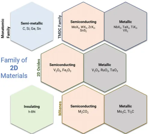
Fig. 1.1 A schematic showing the greater family of 2D materials. Although the great majority
of the 2D materials that has been extensively studied so far belongs to the semiconductors of the TMDCs, there are still hundreds of 2D layers to be investigated
tuning parameter is the formation of the heterostructure of various materials. MoS2 can form both in-plane and van der Waals heterostructures with another 2D material. As recently demonstrated, van der Waals heterostructure of bilayer of a material with a small twist shows distinctly different electrical properties due to formation of the Moiré potentials to modify the energy landscape of the charge carriers.
In terms of electrical conductivity there are insulating, semiconducting, semi-metallic and semi-metallic 2D materials. Among the semiconductors there are famous examples such as MoS2or WS2(or their selenides) where they show direct band gap in the monolayer and indirect band gap from bilayer to bulk. The strong spin-orbit coupling with the broken inversion symmetry leads to optically accessible valley physics. Another commonly studied semiconducting 2D material has been the black phosphorous. It offers a thickness tunable direct bandgap with a high carrier mobility over 1000 cm2/Verses. Despite being unstable in the ambient, the prospects it offers in applications have attracted a great deal of attention. Metallic 2D materials have
1.1 Introduction to Atomically Thin Materials 3 started attracting interest as more and more studies showed high quality contact formation to the semiconducting 2D materials through the edge epitaxy. Moreover, many metallic 2D materials show intriguing properties. The exotic effects observed in the bulk such as superconductivity, charge density waves or Kondo physics typically gets modified as the material thickness approaches to the monolayer limit due to various reasons. As an instance 2H–TaS2 shows superconducting transition at an elevated temperature with the hints of 2D superconductivity in 6 layers [3]. It is also possible to obtain ferromagnetism in the 2D limit in materials such as CrI3and Cr2Ge2Te6. This magnetism can be tuned with the number of layers as well as the external pressure on the sample.
The “periodic table” of 2D materials is yet to be completed and seems like it is going to offer a new “chemistry” that uses 2D layers rather than atoms (Fig.1.1). There are many good literature reviews on the topic and as I would like to focus on the thermal properties of 2D materials on this brief, I will stop the introduction to the 2D materials here and refer the reader to these excellent reviews for further information.
1.2
Obtaining 2D Materials
2D materials can be obtained via various methods. The most commonly employed method is the mechanical exfoliation of atomically thin crystals from the bulk using a sticky tape [1]. This produces very high-quality crystals; however, the yield of the monolayer crystals is sufficient only for proof-of-concept demonstrations. Another commonly used method is the chemical vapor deposition (CVD) of the 2D flakes. This method typically yields lower quality samples as compared to the mechanical exfoliation yet results in large crystals in multiples of numbers. By controlling the growth parameters, it is also possible to obtain wafer large polycrystalline mostly monolayer films. Further improvement in uniformity of the monolayers in CVD can be achieved in metal-organic deposition of the monolayers on substrates like sapphire. However, as demonstrated in many studies dislocations and defects in the grain boundaries in polycrystalline films are prone to oxidation and vastly alters the overall sample properties. Finally, liquid exfoliation is another common method to obtain the monolayers in liquid via intercalating ions in between the layers. The method produces sub-micron sized crystals and not suitable for many applications and proof-of-concept demonstrations.
1.2.1
Mechanical Exfoliation of 2D Materials
Mechanical exfoliation of the 2D materials has been a revolutionary method to inves-tigate atomically thin layers. First of all, it only requires the bulk crystal and a sticky tape. As the intralayer forces are very week, mechanical tape can easily separate the layers from each other. These layers can be deposited on smooth surfaces with
4 1 Atomically Thin Materials
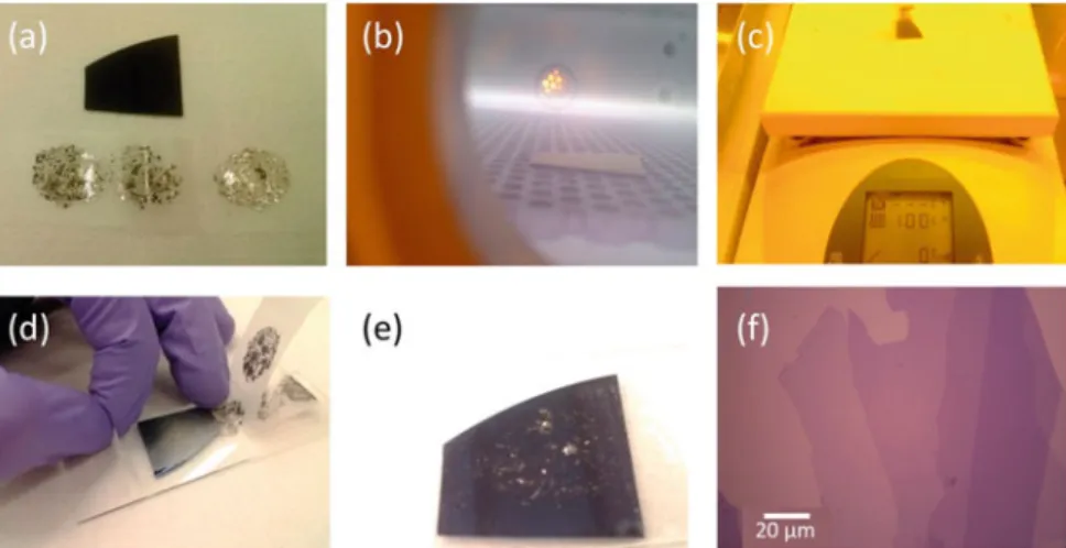
Fig. 1.2 a Tape with the 2D layers exfoliated from the bulk and the oxidized silicon chip is shown. b
and c shows the oxygen plasma treatment of the substrate to increase the adhesion of the monolayers and heated the substrate is heated to remove any water residues. d Adhesion of the tape on the substrate to deposit the monolayers is photographed and e the substrate after mechanical exfoliation.
f Optical microscope micrograph of the substrate shows large layered material. Reprinted with the
permission from Huang et al. [4] Copyright (2015) American Chemical Society
enough attraction by sticking the tape. This produces crystals of varying thicknesses. The yield heavily depends on the substrate, stickiness of the tape and the type of the crystal to be deposited. Moreover, oxidation of the surface further effects the yield of the atomically thin layers to be deposited (Fig.1.2). There are recent efforts that results in reproducible exfoliation [4] of the monolayers up to in centimeter size [5]. As an example gold evaporated stacks of polyvinylpyrrolidone (PVP) with thermal release tape can pick a single monolayer from the bulk crystal and can be deposited on a surface with a subsequent etching of the gold on the top. Type of the tape used is also important in improving the yield. Typically, Nitto brand tape with very low adhesion is used for exfoliation of many materials yet some others require a stickier tape for a higher yield.
Currently, most of the leading laboratories on 2D materials around the world are now performing exfoliation within an inert chamber as even the most oxidation durable materials are adversely affected by the oxygen and the moisture in the ambi-ent. Recent developments in the oxygen and moisture free chambers will most likely to make the process more efficient and cheaper [6]. In particular, the booming interest on the physics of the twisted multi-layer structures namely the Moire superlattices increased the interest in ultra-clean interfaces between the layers [7,8]. Interlayer contamination leads to significant reduction in the electronics of the superlattice.
The sticky tape exfoliation of the 2D layered materials begin with the bulk crystal either mined (typically for graphite or MoS2) or synthesized via chemical vapor transport (CVT) synthesis method. Most of the CVT based synthesis of the bulk material follows a similar recipe. Precursor materials such as the metal and the
1.2 Obtaining 2D Materials 5 chalcogens mixed with a transport agent such as iodine are placed at the opposing sides of a vacuum sealed quartz ampule. Then, a long growth procedure starts with well defined temperature steps. A few millimeter large crystal may take up to a month to form at elevated temperatures. There are several companies that provide the bulk materials such as 2d Semiconductors Inc. (USA) and HQ Graphene (the Netherlands). However, most bulk crystals of 2D materials are notoriously difficult to obtain in the monolayer.
1.2.2
Chemical Vapor Deposition of Monolayers
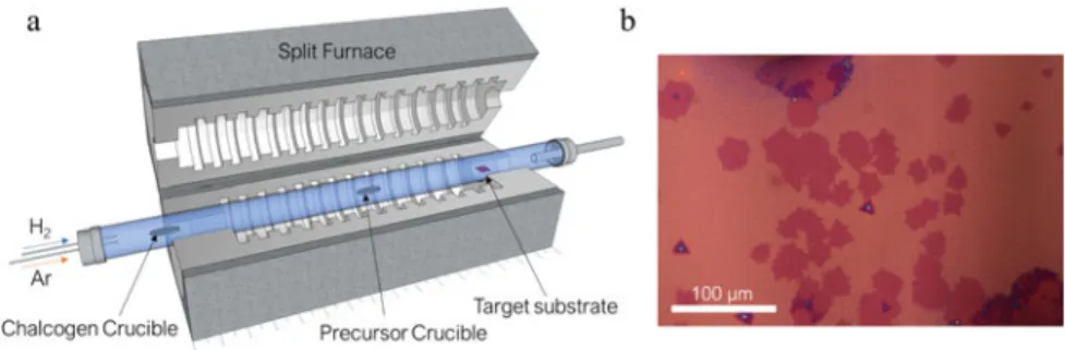
Chemical vapor deposition of monolayer materials begs for an entire book, perhaps several volumes of books. Chemical vapor deposition can be performed in several ways. First of all, it is possible to perform the growth using a vapor-vapor-solid mechanism starting with solid precursors and forming gasses. For instance, MoS2 monolayers can be synthesized using MoO3 and Se precursors with H2 gas on a substrate. It has been shown that if a salt such as NaCl or KI is added to the metal oxide precursor, due to formation of more volatile gaseous and liquid precursors, the nucleation and the growth of the crystals become more controllable. This also enables the synthesis of layered metalchalcogenides from metal precursors with little volatility. It is also possible to use the metalorganic chemical vapor deposition method for wafer-scale synthesis of monolayers. However, the quality of the film is still not at the desired level due to the small grain sizes. Also, the cost of the synthesis is still not justifiable for many applications for the quality of the crystals obtained (Fig.1.3). Finally, I would like to highlight one of the methods we introduced [9]. Using a custom-made chemical vapor deposition chamber with an optical observation win-dow, we enabled the real-time control of the monolayer synthesis. This enables the fabrication of unique heterostructures of 2D materials as well as establishing the required parameters for the crystal growth. The chamber is a cold-walled chamber that is composed of discrete heaters that are designated for heating different
precur-Fig. 1.3 a Schematic of a typical CVD split-tube furnace for 2D materials growth is shown. b A
6 1 Atomically Thin Materials
Fig. 1.4 Figure showing the results of the substrate temperature on the nucleation of MoSe2crystals
on oxidized silicon substrates. This is different than what other studies reported as in conventional CVD chamber it is not possible to change the substrate temperature without creating thermal gradients over the sample or changing the precursor temperatures. Scale bar is 20µm
sors and the substrate that is directly located under an optical window. With an high magnification microscope equipped with 40× objective (ultra-long working distance with cover slip compensation up to 2 mm), high resolution tracking of the growth in-real time is possible. Moreover all the gas flow parameters are controlled via software that enables accurate timing of the reaction gasses. In our paper, we demonstrated the relevant mechanisms for the salt assisted synthesis of MoSe2, WSe2monolayers and their lateral and vertical heterostructures in a single-step. We also characterized the growth rate via vapor-solid-solid and vapor-liquid-solid mechanisms. Moreover, with the chamber we studied the real effect of the substrate temperature on the crystal formation. Unpublished results are shown in Fig.1.4that shows the sole effect of the substrate temperature on the nucleation of the MoS2crystals with all the other parameters are kept constant.
1.2.3
Heterostructures of 2D Materials
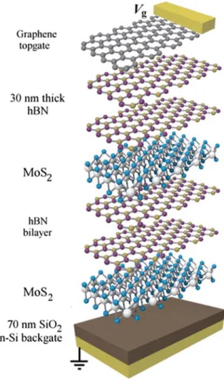
One of the marvels of the modern technology is the layer-by-layer deposition of semiconducting layers with varying band gaps. The deposition of the layers mostly uses molecular beam epitaxy, metalorganic chemical vapor deposition of pulsed laser deposition. This is a research field on its own and it has been a technological break-through. However, deposition of these semiconducting layers is extremely costly due to high purity and ultra-high vacuum conditions required for the deposition of the layers. Similar heterostructures can be fabricated by using 2D materials as well. It is possible to transfer both mechanically exfoliated and CVD grown crystals on various substrates and various other 2D crystals. New functionality can be gained through fabrication of such hetero-structures due to the electronic and phononic
1.2 Obtaining 2D Materials 7 intralayer coupling (Fig.1.5). Unlike the synthesized heterostructures, there is also so-called Moiré degree of freedom that results in novel electronic band formation [7]. The fabrication procedure of the heterostructures are rather straightforward however requires an ultra-clean environment for the best results. Gant et al. [6] recently pub-lished a very comprehensive paper on high quality transfer of 2D materials. I would like to refer the reader to their paper and the reference therein for a more detailed information.
Fig. 1.5 A schematic
showing the stacking of the van der Waals
heterostructure of 2D layers. Reprinted with the permission from Calman et al. [10]. Copyright (2016) AIP Publishing
8 1 Atomically Thin Materials
1.3
A Suitable Platform to Study Fundamental Science and
Explore Applications
In the previous sections I tried to give a brief overview of a wast field. I would like to conclude this chapter by discussing why 2D materials has been so popular in the last decade and a half. Creating non-existing features in solid-state systems require fabrication of carefully designed structures, called superlattices (SL), to be formed in very high quality layers. Most commonly employed method is layer by layer for-mation of these layers using molecular beam epitaxy (MBE). Operation of the MBE is extremely costly and the design of the structures require many iterations. The main reason is the lattice mismatch induced stress on the alternating layers. Thus buffer layers have to be investigated carefully to minimize such stresses to reduce the defect formation for high performance applications. Metal-organic chemical vapor depo-sition (MOCVD) is another commonly utilized method that is relatively cheaper to operate and can be scaled to multiple wafer deposition for industrial processes. How-ever, the defects and impurities in MOCVD grown SLs are much more significant compared to MBE grown SLs. Pulsed laser deposition (PLD) is another method that can be used for evaporation of materials in a controlled way on the target substrate. However, PLD method is somewhat limited in the industrial scale applications and creation of the SLs. Moreover, just like MBE, MOCVD and PLD are very expensive equipment for a research group to have and operate. These reasons form the basis of the boom behind the 2D materials research.
As mentioned in the introduction, 2D materials form a huge family. More than hundreds of 2D materials have been isolated so far. It is possible to form the het-erostructures of these 2D materials to create novel SLs. The major advantage over other SL forming methods is that the 2D crystals can be mechanically exfoliated and at the proof of concept level it is possible to study the basic physics and applications of the SLs. Furthermore, there are new degrees of freedoms that can be employed to gain novel functionality in the SL structure. For instance formation of Moire patterns due to slight rotational angles among the layers results in novel properties in the 2D SL structures. The entry barrier to the field is very low: crystals can be exfoliated from the bulk material using a sticky tape and can be deposited on any suitable substrate. Even the formation of the heterostructures can be done with very high precision at a very low initial and operational cost. This allows many researchers around the world to easily adopt the required methods to study the 2D materials. This is a positive feedback loop. As more researchers enter the field, it becomes more visible and as it becomes more visible more researchers keep entering the field. Still, there are many materials waiting to be discovered with many phenomena waiting to be explored.
1.3 A Suitable Platform to Study Fundamental Science and Explore Applications 9
1.3.1
Applications of 2D Materials
Being a relatively young research field, it is not realistic to expect applications that can compete with concurrent technologies. However, the prospects of applications are quite tantalizing and there are many research groups working on finding ways to make 2D materials commercially viable. This requires high quality materials to be synthesized in wafer scale and possibly the removal of the 2D layer from the growth substrate to form flexible optoelectronics and heterostructures. The major advantage of the 2D materials will become more apparent in the long run with the use of novel degrees of freedom available in these materials. As an instance, valley polarization that exists in inversion symmetry broken semiconducting monolayer provides a way to selectively couple circularly polarized light to the electronic states. Further examples can be given in the field of 2D magnets. These 2D magnets can be controlled depending on the number of layers.
As the focus of this brief is on the thermal conductivity measurements of 2D materials, I would like to conclude this chapter by providing an introduction on the thermal properties of 2D materials. Single crystal graphene flakes are shown to demonstrate very high thermal conductivity in the range of 1450–5300 W/m K [11–13]. Possibility of having such high thermal conductivity values is very promis-ing for heat dissipation applications. Another excitpromis-ing 2D material is the h-BN. Despite being an insulator, it exhibits considerably high thermal conductivity in the vicinity of 300 W/m K [14–16]. To put in a context, thermal conductivity of Si at room temperature is around 130 W/m K and even for copper and silver it is around 400 W/m K. These high thermal conductivity finds its particular use in heat dissi-pation in electronics and cooling applications. Another particularly important side is the ultra-low thermal conductivity measurements for heat shielding and high ZT materials for thermoelectric harvesting. However, as mentioned in the first sections, 2D materials family is a large one and there are many different types of 2D materials that are not measured to date.
References
1. Novoselov KS (2004) Science 306(5696):666. https://doi.org/10.1126/science.1102896.
https://www.sciencemag.org/lookup/doi/10.1126/science.1102896
2. Mounet N, Gibertini M, Schwaller P, Campi D, Merkys A, Marrazzo A, Sohier T, Castelli IE, Cepellotti A, Pizzi G, Marzari N (2018) Nat Nanotechnol 13(3):246.https://doi.org/10.1038/ s41565-017-0035-5.
3. Navarro-Moratalla E, Island JO, Manãs-Valero S, Pinilla-Cienfuegos E, Castellanos-Gomez A, Quereda J, Rubio-Bollinger G, Chirolli L, Silva-Guillén JA, Agraït N, Steele GA, Guinea F, Van Der Zant HS, Coronado E (2016) Nat Commun 7:1.https://doi.org/10.1038/ncomms11043
4. Huang Y, Sutter E, Shi NN, Zheng J, Yang T, Englund D, Gao HJ, Sutter P (2015) ACS Nano 9(11):10612.https://doi.org/10.1021/acsnano.5b04258
5. Liu F, Wu W, Bai Y, Chae SH, Li Q, Wang J, Hone J, Zhu XY (2020) To be published 906(February):1
10 1 Atomically Thin Materials 6. Gant P, Carrascoso F, Zhao Q, Ryu YK, Seitz M, Prins F, Frisenda R, Castellanos-Gomez A
(2020) 2D Materials (2020).https://doi.org/10.1088/2053-1583/ab72d6
7. Cao Y, Fatemi V, Fang S, Watanabe K, Taniguchi T, Kaxiras E, Jarillo-Herrero P (2018) Nature 556(7699):43.https://doi.org/10.1038/nature26160
8. Cao Y, Fatemi V, Demir A, Fang S, Tomarken SL, Luo JY, Sanchez-Yamagishi JD, Watanabe K, Taniguchi T, Kaxiras E, Ashoori RC, Jarillo-Herrero P (2018) Nature 556(7699):80.https:// doi.org/10.1038/nature26154
9. Rasouli HR, Mehmood N, Çakıro˘glu O, Kasırga TS (2019) Nanoscale 11(15):7317.
https://doi.org/10.1039/C9NR00614A. http://pubs.rsc.org/en/Content/ArticleLanding/2019/ NR/C9NR00614A,http://xlink.rsc.org/?DOI=C9NR00614A
10. Calman EV, Dorow CJ, Fogler MM, Butov LV, Hu S, Mishchenko A, Geim AK (2016) Appl Phys Lett 108(10):101901.https://doi.org/10.1063/1.4943204
11. Balandin AA, Ghosh S, Bao W, Calizo I, Teweldebrhan D, Miao F, Lau CN (2008) Nano Lett 8(3):902.https://doi.org/10.1021/nl0731872
12. Chen S, Moore AL, Cai W, Suk JW, An J, Mishra C, Amos C, Magnuson CW, Kang J, Shi L, Ruoff RS (2011) ACS Nano 5(1):321.https://doi.org/10.1021/nn102915x
13. Cai W, Moore AL, Zhu Y, Li X, Chen S, Shi L, Ruoff RS (2010) Nano Lett 10(5):1645.https:// doi.org/10.1021/nl9041966
14. Jo I, Pettes MT, Kim J, Watanabe K, Taniguchi T, Yao Z, Shi L (2013) Nano Lett 13(2):550.
https://doi.org/10.1021/nl304060g
15. Zhou H, Zhu J, Liu Z, Yan Z, Fan X, Lin J, Wang G, Yan Q, Yu T, Ajayan PM, Tour JM (2014) Nano Res 7(8):1232.https://doi.org/10.1007/s12274-014-0486-z
16. Cai Q, Scullion D, Gan W, Falin A, Zhang S, Watanabe K, Taniguchi T, Chen Y, Santos EJ, Li LH (2019) Sci Adv 5(6):1.https://doi.org/10.1126/sciadv.aav0129