A THESIS
SUBMITTED TO THE DEPARTMENT OF PHYSICS
AND THE GRADUATE SCHOOL OF ENGINEERING AND SCIENCES OF BILKENT UNIVERSITY
IN PARTIAL FULFILLMENT OF THE REQUIREMENTS FOR THE DEGREE OF
DOCTOR OF PHILOSOPHY
By
Serkan Bütün
December 2011
ii
I certify that I have read this thesis and that in my opinion it is fully adequate, in scope and in quality, as a thesis for the degree of Doctor of Philosophy.
Prof. Dr. Ekmel Özbay (Supervisor) I certify that I have read this thesis and that in my opinion it is fully adequate, in scope and in quality, as a thesis for the degree of Doctor of Philosophy.
Prof. Dr. Süleyman Özçelik I certify that I have read this thesis and that in my opinion it is fully adequate, in scope and in quality, as a thesis for the degree of Doctor of Philosophy.
Assoc. Prof. Dr. Ceyhun Bulutay I certify that I have read this thesis and that in my opinion it is fully adequate, in scope and in quality, as a thesis for the degree of Doctor of Philosophy.
Assoc. Prof. Dr. M. Özgür Oktel I certify that I have read this thesis and that in my opinion it is fully adequate, in scope and in quality, as a thesis for the degree of Doctor of Philosophy.
Assit. Prof. Dr. Ali Kemal Okyay
Approved for the Graduate School of Engineering and Sciences:
Prof. Dr. Levent Onural
iii
ABSTRACT
AlGaN UV PHOTODETECTORS: FROM MICRO TO
NANO
Serkan Bütün PhD in Physics
Supervisor: Prof. Dr. Ekmel Özbay
December, 2011
The absorption edge of AlGaN based alloys can be tuned from deep UV to near UV by changing the composition. This enables the use of the material in various technological applications such as military, environmental monitoring and biological imaging. In this thesis, we proposed and demonstrated various UV photodetectors for different purposes. The multi-band photodetectors have the unique ability to sense the UV spectrum in different portions at the same time. We demonstrated monolithically integrated dual and four-band photodetectors with multi layer structures grown on sapphire. This was achieved through epitaxial growth of multi AlGaN layers with decreasing Al content. We suggested two different device architectures. First one has separate filter and active layers, whereas the second one has all active layers which are used as filter layers as well. The full width at half maximum (FWHM) values for the dual band photodetector was 11 and 22 nm with more than three orders of magnitude inter-band rejection ratio. The self-filtering four band photodetector has FWHMs of 18, 17, 22 and 9 nm from longer to shorter bands. Whereas photodetector with separate filter layers has FWHMs of 8, 12, 11 and 8 nm, from longer to shorter bands. The overall inter-band rejection ration was increased from about one to two of magnitude after incorporating the passive filter layers. The plasmonic enhancement of photonic devices has attracted much
iv
attention for the past decade. However, there is not much research that has been conducted in UV region. In the second part of this thesis, we fabricated nano-structures on GaN based photodetectors and improved the responsivity of the device. We have fabricated Al nano-particles on sapphire with e-beam lithography. We characterized their response via spectral extinction measurements. We integrated these particles with GaN photodetectors and had enhancement of %50 at the plasmonic resonance of the nano-particles. Secondly, we have fabricated sub-wavelength photodetectors on GaN coupled with linear gratings. We had 8 fold enhancement in the responsivity at the plasmonic resonance frequency of the grating at normal incidence. Numerical simulations revealed that both surface plasmons and the unbound leaky surface waves played a role in the enhancement. We, finally, conducted basic research on the current transport mechanisms in Schottky barriers of AlGaN based materials. Experiments revealed that the tunneling current plays a major role in current transport. In addition incorporation, of a thin insulator between metal-semiconductor interface reduces the undesired surface states thereby improving the device performance.
Keywords: AlGaN, GaN, photodetector, multi-band, dual-band, MSM,
Schottky, plasmonics, surface plasmon polariton, grating, nano-particle , localized surface plasmon resonance
v
ÖZET
AlGaN UV FOTODEDEKTÖRLER: MİKRODAN
NANOYA
Serkan Bütün Fizik doktora
Tez Yöneticisi: Prof. Dr. Ekmel Özbay
Aralık, 2011
AlGaN temelli alaşımların soğurma kesimi Al oranı değiştirilerek derin UV dalgaboylarından yakın UV dalgaboylarına kadar ayarlanabilir. Bu özellik, malzemeyi, askeri, çevresel ve biyolojik görüntüleme gibi pek çok teknolojik alanlarda kullanma imkanı sağlamaktadır. Bu çalışmamızda, farklı uygulamalara yönelik UV fotodedektörler tasarladık ve ürettik. Çoklu bantlarda soğurma yapabilen dedektörler UV ışığı farklı dalgaboylarında algılayabilmektedirler. Bu amaçla, tek seferde büyütülmüş çoklu AlGaN katmanları üzerinde iki ve dört bantlı fotodedektörler ürettik. Bu, yukarı doğru azalan Al oranlarında AlGaN katmanları büyütülerek sağlandı. İki farklı tipte aygıt tasarımı yapıldı. Birinci tipte fotodedektör dört aktif soğurma katmanından oluştu. Her katman aynı zamanda diğer bantlar için filtre görevi gördü. İkinci tipte ise, her bant için farklı Al oranında bir aktif soğuma ve bir pasif filtre katmanı vardı. İki bantlı fotodedektörün her bandı için yarı doruk genişliği (YDG) kısa ve uzun bantlar için sırasıyla 11 ve 22 nm olarak ölçüldü. Bantlar arası bin kattan fazla kontrast ölçüldü. Birinci tip dört bantlı fotodedektör uzun banttan kısa banda doğru 18, 17, 22 ve 9 nm YDG gösterirken ikinci tip dört bantlı fotodedektör 8, 12, 11 ve 8 nm YDG gösterdi. Ayrıca bantlar arası kontrast on kattan yüz kata çıktı. Fotonik aygıtların plazmonik yapılarla güçlendirilmesi geçtiğimiz on yıldır çok ilgi çekmektedir. Fakat UV bölgede, bu konuda yapılmış çalışma hemen hemen
vi
hiç yoktur. Çalışmamızın ikinci kısmında ürettiğimiz çeşitli nano-yapıları GaN fotodedektörler ile bütünleştirdik ve fotodedektör cevabında bir iyileşme gözlemlerdik. Elektron mikroskobu ile safir üzerine Al nano-parçacıklar ürettik. Spektral geçirgenlik ölçümleri ile bu parçacıkların karakterizasyonu yaptık. Aynı nano-parçacıkları GaN fotodedektörler üzerine koyduğumuzda dedektör cevabında bir buçuk kata varan iyileşme gözlemledik. İkinci olarak, dalgaboyu altı fotodedektörler ürettik. Bu dedektörleri Al kırınım ağı ile bütünleştirdik. Kırınım ağının plasmonik çınlama dalgaboyu civarcında yüzeye dik aydınlatma ile fotodedektör cevabında sekiz kata varan bir iyileşme tespit ettik. Bilgisayar simülasyonları bu iyileşmenin hem yüzey plazmonlarına hem de yüzeyde oluşan sızıntı radyasyonuna bağlı olduğunu gösterdi. Son olarak AlGaN temelli malzemelerde Schottky tipi bariyerlerindeki akım mekanizmalarını inceleyen temel araştırmalar yaptık. Sonuçlara göre baskın akım mekanizmasının tünelleme akımı olduğu tespit edildi. Ayrıca metal-yarıiletken arayüzüne koyulacak ince yalıtkan katmanların istenmeyen ara-yüzey enerji seviyelerini düşürdüğü ve bu sayede aygıt performansını artırdığı gözlenmiştir.
Anahtar sözcükler: AlGaN, GaN, photodetector, çoklu bant, iki-bant, MSM, Schottky, plazmonik, yüzey plazmon polaritonları, kırınım ağı, nano-parçacık, sınırlandırılmış yüzey plazmon çınlamaları.
vii
Acknowledgements
I am honored to present my sincere gratitude to my supervisor Prof. Dr. Ekmel Özbay for his endless support, guidance, motivation and encouragement during this research. I was a life time experience and such a great honor to work with him.
I would like to thank to Prof. Dr. Süleyman Özçelik, Assoc. Prof. Dr. Ceyhun Bulutay, Assoc. Prof. Dr. Mehmet Özgür Oktel, and Asst. Prof. Dr. Ali Kemal Okyay for being in my thesis committee. I am grateful for their valuable time and comments for evaluating this thesis.
I would like to thank to all the former and present personnel of the Nanotechnology Research Center for being good friends, understanding and making life easier. I would like to thank specifically Dr. Mutlu Gökkavas for his help, valuable experiences and suggestions especially in multi color photodetector work. I am indepted to Mrs. Neval Ayşegül Cinel for her help in simulations of the plasmonic structures. I would also like to thank Dr. HongBo Yu on behalf of the MOCVD team. This work would not be possible without their efforts. I appreciate the efforts of Dr. Engin Arslan in our work on Schottky barriers for modeling our measurements.
I also would like to mention the help of some people in Semiconductor Technologies Advanced Research Lab of Gazi University, Prof. Dr. Semsettin Altındal, Dr. Sefer Bora Lişesivdin, Mrs. Yasemin Safak, Mrs. Habibe Uslu and Mr. Ilke Tasçıoglu for their parts in C-V measurements as well as comments in our collaborations.
I also thank to all the former and present faculty members and personnel of the Advanced Research Laboratory and the Department of Physics. It was an honor to work aside with these hardworking people. Another special thank goes here to Mr. Murat Güre and Ergun Kahraman for their technical support and guidance in the laboratory.
viii
I hereby would like to acknowledge and extend my heartfelt gratitude to the following persons with whom I made personal acquaintance with in Özbay group, Advanced Research Laboratory and the department of Physics during my Ph.D. Dr. Dündar Yılmaz, Dr. Koray Aydın, Dr. Hümeyra Çağlayan, Dr. Bayram Bütün, Dr. Turgut Tut, Dr. Kamil Boratay Alıcı, Dr. Funda Tamara Gündoğdu, Dr. Irfan Bulu, Dr. Aşkın Kocabaş, Mr. Deniz Çalışkan, Mr. Atilla Özgür Çakmak, Mr. Evrim Çolak, Mr. Hüseyin Çakmak, Mr, Semih Çakmakyapan, Mr. Özgür Kazar, Mr. Erkin Ülker, Mr. Mustafa Öztürk, Mrs. Pakize Demirel and many more, I thank you all for your friendship and valuable suggestions.
I am indebted to my parents and my brother for their love, encouragement and support.
Finally, I dedicate this work to my wife and my son. I am so much thankful for their love, endless trust and bringing joy to my life.
ix
Contents
ABSTRACT ... iii ÖZET ... v Acknowledgements ... vii Contents ... ixList of Figures ... xiii
List of Tables ... xvi
Chapter 1 Introduction ... 1
1.1 Motivation ... 4
1.2 Organization of the thesis ... 5
Chapter 2 Theoretical Background ... 6
2.1 A brief introduction to semiconductor physics ... 6
2.1.1 Electrical properties ... 6
2.1.2 Optical properties ... 8
2.1.3 The Schottky Junction ... 9
2.2 MSM photodetectors ... 11
2.2.1 Characterization of the photodetectors ... 12
2.3 Fundamentals of surface plasmon polaritons ... 13
2.3.1 Surface plasmon polaritons ... 13
2.3.2 Localized surface plasmon resonance ... 17
x
3.1 Introduction ... 20
3.2 Dual-Color sensing UV photodetectors ... 21
3.2.1 Concept ... 22
3.2.2 Fabrication and Results ... 23
3.2.3 Conclusion ... 30
3.3 Four-Color sensing UV photodetectors ... 31
3.3.1 Concept ... 32
3.3.2 Fabrication and Results ... 32
3.3.3 Conclusion ... 42
3.4 Four-Color sensing UV photodetectors with extra filter layers 42 3.4.1 Concept ... 43
3.4.2 Fabrication and Results ... 43
3.4.3 Conclusion ... 47
Chapter 4 UV Sensitive Nano-structured Photodetectors ... 49
4.1 Introduction ... 49
4.2 LSPR enhanced MSM UV photodetectors ... 50
4.2.1 Introduction ... 50
4.2.2 Fabrication and Results ... 51
4.2.3 Conclusion ... 54
4.3 Sub-wavelength UV photodetector with integration of a nanoantenna ... 56
4.3.1 Introduction ... 56
4.3.2 Fabrication of the Plasmonic Photodetectors ... 57
xi
4.3.4 FDTD Simulations ... 62
4.3.5 Conclusion ... 64
Chapter 5 Current Transport Mechanism Investigations of AlGaN Based Heterostructures ... 66
5.1 Current transport mechanisms and trap state investigations in (Ni/Au)-AlN/GaN Schottky barrier diodes ... 66
5.1.1 Introduction ... 67
5.1.2 Fabrication and Results ... 68
5.1.3 Conclusions ... 77
5.2 Electrical characterization of MS and MIS structures on AlGaN/AlN/GaN heterostructures ... 78
5.2.1 Introduction ... 78
5.2.2 Fabrication an Results ... 80
5.2.3 Conclusions ... 93
5.3 Leakage current investigation of Ni/Au Schottky contacts on GaN based heterostructures ... 94
5.3.1 Introduction ... 94
5.3.2 Fabrication and Results ... 95
5.3.3 Conclusion ... 98
Chapter 6 Conclusion ... 100
Bibliography ... 103
Appendix ... 116
A. Microfabrication techniques used in this study ... 116
A1. Sample Preparation ... 116
xii
A3. Etching ... 118
A4. Metallization ... 118
A5. Dielectric Coating ... 118
B. Nanofabrication techniques used in this study ... 119
B1. E-beam lithography ... 119
xiii
List of Figures
Figure 2.1: Energy bands of wurtzite GaN along symmetry lines of the
Brillouin zone. (adopted form[73]) ... 7
Figure 2.2: Absorption coefficient of AlxGa1-xN epitaxial films grown on sapphire. (adopted from [76]) ... 9
Figure 2.3: Band diagram of a metal-semiconductor-metal photodetector. ... 10
Figure 2.4: Dielectric permittivity functions of metals ... 14
Figure 2.5: Dispersion relation of the SPPs on Al/Air interface. ... 16
Figure 2.6: Extinction spectra of Al nano-spheres in air. ... 19
Figure 3.1: Conceptual drawing of the dual color MSM photodetector cross-section. ... 22
Figure 3.2: Spectral transmission measurements: ... 25
Figure 3.3:IV characterization of the dual color photodetectors ... 28
Figure 3.4: Spectral responsivity measurements of the dual-color photodetectors. ... 29
Figure 3.5: Schematic diagram of the spectral photoconductivity setup ... 31
Figure 3.6: Schematic illustration of how a four-band photodetector works. .... 33
Figure 3.7: Fabrication of the four-band photodetectors. ... 34
Figure 3.8: Spectral transmission measurements of the wafer 1. ... 34
Figure 3.9: Normalized Quantum efficiency of the photodetector ... 36
Figure 3.10: IV Measurements of the four band photodetector ... 38
Figure 3.11: Comparison of the spectral response and the transmission measurements. ... 40
Figure 3.12: IV measurements of the fabricated photodetectors on sample 2. The numbers denote the quadrants from top to bottom. ... 41
xiv
Figure 3.13: Spectral transmission measurements of the recess etched 8
layered sample. ... 44
Figure 3.14: Spectral normalized quantum efficiency measurements of the four-color sample with extra filter layers. ... 46
Figure 3.15: Spectral responsivity measurements of the four-color photodetector with extra filter layers in log scale. ... 46
Figure 3.16: Leakage current characteristics of the four-color photodetector with filter layers. ... 47
Figure 4.1: Conceptual drawing of an LSPR enhanced MSM photodetector. (viewed from the top) ... 51
Figure 4.2: A photograph of the micro-transmission setup. ... 52
Figure 4.3: Fabricated Al nano-particles: ... 53
Figure 4.4: Spectral quantum efficiency measurement of LSPR enhanced photodetector along with the control sample. ... 55
Figure 4.5: Enhancement of the quantum efficiency with Al nano-particles. .... 55
Figure 4.6: Conceptual drawing of the nano-structured MSM photodetector ... 59
Figure 4.7: Characterization and the optimization of the plasmonic gratings. .. 60
Figure 4.8: The fabrication and the measurements of the subwavelengt photodetectors. ... 62
Figure 4.9: Numerical simulations of the designed grating structures. ... 64
Figure 5.1: The J–V characteristics of (Ni/Au)–AlN/GaN SBDs. ... 70
Figure 5.2: The fitting of the tunneling current expression ... 71
Figure 5.3: The temperature dependences of the tunneling saturation current density (Js_tunnel) and the characteristic energy of tunneling (E00) for (Ni/Au)-AlN/GaN SBDs. ... 72
xv
Figure 5.4: (a) Typical measured capacitance and (b) conductance data as a function of voltage for (Ni/Au)–AlN/GaN SBDs measured at 0.7, 1, 2, and 3 kHz. ... 73 Figure 5.5: Equivalent circuit model of (Ni/Au)–AlN/GaN SBDs used to
extract trap parameters from the experimental measurements. ... 74 Figure 5.6: Parallel conductance as a function of frequency for (Ni/Au)–
AlN/GaN SBDs at different bias voltage values. ... 75 Figure 5.7: Experimentally derived density (Dt) and time constants (ηt) of
the trap statesas a function of energy separation from the conduction-band edge (Ec - Et). for (Ni/Au)–AlN/GaN SBDs. ... 76
Figure 5.8: AFM surface topography images of the SBD HEMTs ... 83 Figure 5.9: Forward and reverse bias semi-logarithmic I-V characteristics of
SBD HEMT and MIS HEMTs. ... 83 Figure 5.10: The I-V analysis of the SBDs. ... 87 Figure 5.11: Density of interface states Nss as a function of Ec-Ess ... 89 Figure 5.12: The measured (a) C–V and (b) G/ω–V characteristics of SBD
HEMTs and MIS HEMTs measured at 1 MHz ... 92 Figure 5.13: Density of interface states Nss as a function of Ec–Ess ... 93 Figure 5.14: Schematic presentation of the fabricated AlInN device used for
the leakage current investigation. ... 96 Figure 5.15: Temperature dependent IV characteristics of Ni/Au Schottky
contacts on AlInN. ... 98 Figure 5.16: Measured reverse-bias current density divided by electric field
vs. square root of electric field. ... 99 Figure 5.17: Temperature dependence of the slope and intercept functions f1
xvi
List of Tables
Table 3.1: Epitaxial layer content of the dual-color photodetector wafer. ... 26 Table 3.2: The summary of the epitaxial structure of the sample 1 for the
four color photodetector. ... 35 Table 3.3: The summary of the epitaxial structure of the sample 2 for the
four color photodetector. ... 38 Table 3.4: Bias conditions and the measured peak responsivity, quantum
efficiency with corresponding FWHM values of the four-color UV photodetector of sample 2. ... 41 Table 3.5: The summary of the epitaxial structure of the eight layer for the
four color photodetector with extra filter layers. ... 45 Table 3.6: Bias conditions and the measured peak responsivity, quantum
efficiency with corresponding FWHM values of the four-color UV photodetector with filter layers. ... 45 Table 5.1: Temperature dependent values of the tunneling saturation current
density ... 70 Table 5.2: The summary of the epitaxial structure of the Al0.22Ga0.78N wafer. . 81 Table 5.3: The passivation layer thickness dependent values of parameters
determined from I-V characteristics of SBD HEMTs and MIS HEMTs. ... 85 Table 5.4 The summary of the epitaxial structure of the Al0.83In0.17N wafer. .... 96
1
Chapter 1
Introduction
The interest in capturing the light dates way back into the history. The early notes mentioning of camera obscura1 are found in ancient China by Mo-Ti[1] (470 to 390 BC). Later Greek philosopher Aristotle (384 to 322 BC) explained [2] the operation principles of the camera. After the photochemicals such as silver nitrate and silver chlorite had been discovered, around 13th to 18th centuries, Niepce accomplished the fixing the image on a metal plate in 1826[3]. After the discovery of the effect of light on the conductivity of selenium and then of the photoelectric effect by Hertz[4] the photomultiplier tubes (PMT) were invented in 1934[5]. The main kicker in those days was the urgent need for a television camera. On the other hand, solid state photodetectors were investigated intensively after the semiconductors emerged around mid-nineteens. Today, we have many types of photodetectors based on semiconductors such as photodiodes from UV to terahertz regimes, charged coupled devices and CMOS sensors.
The earliest reference to the ultraviolet (UV) radiation was in the beginning of 19th century by Thomas Young’s experiments in which he showed the wave nature of this invisible radiation. Typically wavelengths of 100 to 400 nm are considered as UV. It is a highly ionizing radiation with its energy higher than 3.1 eV. The spectrum further divided in to three sub-regions although it covers relatively small portion of the whole electromagnetic spectrum. This is because even a small change in the energy of the UV radiation may result in diverse effects on biological or chemical substances. Usually, the region from 400 to 320 is referred as UVA, 280 to 320 nm is referred as UVB and 100 to 280 nm is referred as UVC.[6] Wavelengths below 280 nm is often regarded as
1 Camera obscura is the first camera which uses a pinhole to project an image on a screen in a dark environment.
the solar blind region since the stratospheric ozone layer absorbs almost all of the radiation in this region. Natural UV sources are very hot objects like the sun. The 9% of the solar radiation from the sun falls in to the UV spectrum [7]. Each subdivision has different effects on earth. For instance, UVA radiation stimulates the photosynthesis, and has some role in the synthesis of some vitamins. However prolonged exposures may lead to sunburn and premature aging. UVB is very detrimental for living species. It causes skin cancer, acute sunburns and cataracts. However, it activates the vitamin D. UVC is the most dangerous of all three. It can ionize the DNA thereby cause severe mutations. Nevertheless all of the radiation from the sun in this range is absorbed by ozone layer.[7]. Therefore it is crucial to have photosensitive receptors working in different portions of the UV radiation.
UV monitoring has many potential civil and military applications. For instance in situ temperature monitoring in nuclear power plants and internal combustion engines, telecommunication (inter-satellite communication in particular), secure non-line of sight communication, ozone layer monitoring, bio-chemical agent detection, instrument calibration for UV lithography, missile plume detection etc.[8, 9]
One must use wide band gap materials so as to detect UV radiation. Optoelectronics based on widely used Si and GaAs can operate in the UV region. However their absorption is very limited. They cannot withhold the severe conditions such as high temperature and high levels of radiation as nearby the most of the UV sources [8]. In addition they are intrinsically responsive to the visible and near infrared (IR) radiation. Therefore it is better to use a material which is intrinsically immune to the visible and IR radiation.
III-V nitrides have attracted much attention in the last couple of decades. Their room temperature direct band gaps (3.4 eV GaN, 6.2 eV AlN and 1.9 eV InN) promises very wide range optoelectronic devices. AlGaN alloys, in particular, have the ability to tune the band edge from 360 to 190 nm by varying Al mole fraction. Moreover, their direct band gap allows the precise tunability
of the material with a sharp cut off. They are immune to aging due to the high energetic radiation compared to the narrow band gap materials. Their resistance to high electric field is higher due to the wide band gap which makes them further beneficial for down scaling to the sub-micron dimensions[7, 10, 11].
UV photodetectors based on AlBxBGaB1-xBN have been reported after the first
successful demonstration of UV photodetectors [12, 13], such as the Schottky barrier [14, 15], p – i – n [16-18], and MSM [19-27] photodetectors.
Optoelectronic devices are getting smaller for better performance in terms of sensitivity, spatial resolution and high speed operation along with the technological developments. The nano-scaled integrated circuit elements have gained much attention due to the demand from the market for flexible, faster and more responsive electronic components. The down side of this miniaturization of the individual circuit elements, however, is the reduction of the absorption cross section for photodetectors in particular. Furthermore, when the device size is shorter than the wavelength, diffraction limits the amount of detectible radiation [28-31].
An intelligently designed plasmonic antenna can overcome this problem [32]. Surface plasmons (SP) are known as coupled plasma oscillations in metal-dielectric interfaces. The effective wavelength of bound surface plasmons is significantly less than the free space wavelength of the radiation[33]. Therefore light can be localized in a more confined volume with the help of the SPs. The experiments of Ebbessen et al.[34-39] have shown that light can be focused down to nearly 10% of its free space wavelength. There are many both experimental and theoretical reports indicating the enhanced responsivity of a photodetector is due to the excitation of surface plasmons [40-46] incorporating the extraordinary light transmission phenomenon. However it is not yet clear whether this enhancement is because of the surface plasmon excitation or leaky surface waves [47].
Localized surface plasmon resonance (LSPR) is a manifestation of SPs on nano-sized metallic particles. SPs interfere constructively at a resonance
frequency depending on the size and the shape of the particle. Thus, a strong extinction is apparent in the transmission spectrum of the nano-particles [48]. This extinction causes the localization of the electric field at the resonance frequency near the vicinity of the particle. This property has led the use of metal nano-particles in many applications such as surface enhanced Raman scattering [49-52] and biosensing [52-61]. There are also reports suggesting that this localized field can as well enhance the light absorption in the vicinity of the nano-particles for thin film and organic photovoltaics [62-71].
1.1 Motivation
The demand for UV optoelectronics has been expanding each day. The developments in the sensor technologies require devices working in very diverse spectrum. Therefore improving the performance and the functionality of UV photodetectors will fulfill the needs of the industry for the innovated products. A monolithically integrated multi-color UV sensor will significantly increase the radiation sensing capability of a photodetector as well as the simplicity of usage in comparison with the separate devices.
On the other hand making sub-wavelength sized devices has many physical insights as well as potential applications. Most of the work done in solar cells and photodetectors were, at most, in the red. This is mostly due to inadequacy of the dielectric constant of the commonly used metals Au and Ag. There is a huge gap from red to UV. By fabricating a nano-patterned antenna on top of a GaN photodetector, we were able to enhance the responsivity by eight-fold. The effective size of the photodetector was less than half of the incident wavelength.
We demonstrated that if one used Al nano-particle on a UV sensitive photodetector instead of Au or Ag, a plasmonic enhancement in UV can be attained. We further proved this enhancement via numerical simulations. This demonstration proves experimentally that LSPR can be utilized from UV to IR.
In addition, we have preformed more fundamental investigations on current transport mechanisms of the Ni-AlGaN based Schottky contacts for a deeper understanding since all of our photodetectors involve Schottky contacts. The investigation revealed that tunneling current is mostly the dominant on these contacts. Therefore operating temperature is less effective on device performance as opposed to the thermionic emission.
1.2 Organization of the thesis
We give a brief theoretical background in the chapter 2. The basic semiconductor physics and the principles of the MSM photodetector are covered first. Then, an overview of surface plasmon polaritons is provided.
In the chapter 3, we present our results on multi-color sensitive UV photodetector. First we discuss the dual color sensitive device. Then we compare our results of two different 4-color devices.
The nano-structure decorated UV photodetectors are discussed in the chapter 4. The first part is dedicated to LSPR enhanced GaN photodetectors. We present the nano-antenna integrated photodetector in the second part.
The investigations on the current transport mechanism of AlGaN based Schottky contacts are given in chapter 5. Current transport mechanisms and trap state investigations in (Ni/Au)-AlN/GaN Schottky barrier diodes are discussed in the first part. Then electrical characterization of MS and MIS structures on AlGaN/AlN/GaN heterostructures is covered. In the end, leakage current investigation of Ni/Au Schottky contacts on GaN based heterostructures is presented.
We give our final remarks and possible future directions of this study in Chapter 6.
We provided detailed fabrication steps used throughout this study in the Appendix.
6
Chapter 2
Theoretical Background
2.1 A brief introduction to semiconductor physics
A semiconductor is defined as a chemical element or a compound that has the electrical conductivity, ζ, higher than the insulators and lower than the common metals. The most common form of the semiconductors is the crystalline solids. Electrons have only certain bands in these materials due to the symmetric arrangement of the atoms in the crystal (Figure 2.1). The void between the uppermost valance band and the lower most conduction band is called the band gap of the semiconductor. That is, the minimum energy required to excite an electron from ground state to a conduction band is equal to the band gap and is usually expressed in terms of eV.In this chapter we will discuss the electrical and optical properties of semiconductors (mostly in the context of GaN). Thereafter, we will briefly discuss the Schottky junction.
2.1.1 Electrical properties
The electronic band structure (E-k relation) of a semiconductor is obtained by solving the Schrödinger equation. Bloch theorem states that if the potential, V(r), is periodic with the periodicity of the lattice, the solution of the Shrödinger equation
(2.1)
are of the form
where Un(k,r) is periodic in r with the periodicity of the direct lattice and n is the
band index [72].
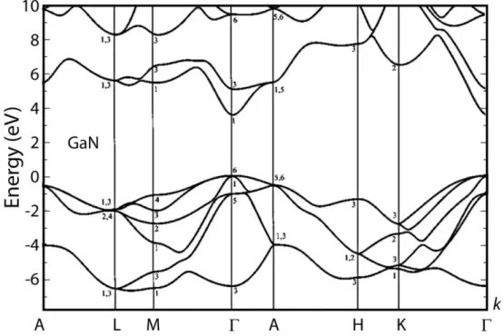
Figure 2.1: Energy bands of wurtzite GaN along symmetry lines of the Brillouin zone. (adopted form[73]1)
There are many numerical methods for calculating the band structure of the semiconductors. For instance, Yeo et al. calculated the band structure of GaN using empirical pseudopotential method. (Figure 2.1). They predicted the band gap of GaN as 3.42 eV.
2.1.1.1 The Band-gap of AlxGa1-xN
The band gap of AlxGa1-xN with respect to Al concentration x is calculated with the empirical formula
(2.3) where b (0<b<1) is the bowing parameter which is measured experimentally. There are a number of values for b reported in the literature [74]. In this work we used b = 0.62 eV.
1 Permission obtained from AIP under the license number 2800490336991. A copy of the license agreement is attached at the end of this thesis.
2.1.2 Optical properties
The interactions between photons and the electrons in a semiconductor form the basics of the technologies such as telecommunication, solid state lighting, and sensing [75]. There are many mechanisms involved in the absorption process such as interband and intraband transitions and exitonic effects. Intraband absorption mechanism is often described with a Drude-like model where a sinusoidal electric field interacts with electrons and holes. Interband absorption which involves transitions from valance band to conduction band is the most important process, which is the basis for solid state photodetectors and emitters. Excitonic effects, in addition, explain the behavior of the absorption coefficient near the band edge.
The absorption coefficient is usually determined with various measurements rather than the numerical calculation. The most common method is spectral reflectance/transmittance measurements. Reflection and the transmission coefficients for normal incidence are given by [72]
(2.4) (2.5)
where, w and λ are the thickness of the sample and the wavelength of the incident light, respectively. n and k are real and the imaginary parts of the index of refraction respectively. The absorption coefficient per unit length is than defined by
(2.6)
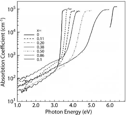
The absorption coefficient can be determined by analyzing T(λ) and R(λ). Brunner et al. measured the absorption coefficient of AlGaN films grown on sapphire with different Al content using transmission and photothermal
deflection spectroscopy [76]. We used these values as a reference for our AlGaN films in this thesis.
Figure 2.2: Absorption coefficient of AlxGa1-xN epitaxial films grown on sapphire.
(adopted from [76]1)
2.1.3 The Schottky Junction
Schottky junction (also known as metal-semiconductor junction) is made up of a metal and a semiconductor material. The name is given after W. Schottky who explained the rectifying behavior of this type of contact in 1930.
1 Permission obtained from AIP under the license number 2800490798464. A copy of the license agreement is attached at the end of this thesis.
Figure 2.3: Band diagram of a metal-semiconductor-metal photodetector.(a) at zero bias and (b) at a bias of V=VF=VR. Here the Fermi level, shown as dashed line, illustrated close to the conduction band because our GaN substrate is intrinsically n-type.
When a metal and a semiconductor are in contact, Fermi levels coincide in thermal equilibrium (See Figure 2.3a).This causes a built in potential, ϕB,
between the contacts. This barrier is expressed as
) (2.7)
where ϕm, and χ are the work function of the metal and the electron affinity of
the semiconductor, respectively and e is the elementary charge. Under the abrupt junction approximation the depletion width W is given as,
(2.8) where V is the applied bias voltage. There are mainly four current transport mechanisms in Schottky junctions. Such as thermionic emission – transport of electrons over the barrier (common for moderately doped semiconductors), quantum mechanical tunneling – important for heavily doped semiconductors,
recombination in space charge region and recombination in neutral region under forward bias.
The thermionic emission current density can be expressed as
(2.9)
(2.10)
where A** is the effective Richardson constant and J
S, is the saturation current
density.
When the tunneling current become the dominant mechanism in the current transport, the current density may be expressed as
(2.11)
where E00 is the characteristic tunneling energy that is related to the tunnel effect
transmission probability and JtS is the tunnel saturation current density.
For detailed derivation of the equations (2.7) through (2.11) please refer to the reference [72].
2.2 MSM photodetectors
Metal-semiconductor-metal (MSM) photodetectors are very easy to realize especially in materials like AlGaN/GaN. Due to growth complexities it is very difficult to grow complex epitaxial structures. In contrary, MSM devices just require a single epitaxial layer. Moreover the fabrication of these kinds of devices is straightforward. They are compatible with integrated circuit processing and suitable for high speed applications. Despite of these nice properties, there is problem due to the basic properties of metals. Metals are very good reflectors of the electromagnetic radiation. In addition skin depth values for metals are very small (~15-20 nm). Therefore in MSM structures only the half of the light can reach through the semiconductor. There are two possible
solutions to overcome this problem. First one is to make the electrodes as thin as possible so that they can transmit as much light as possible. The other method is back illumination of the device. But in this case your substrate and underlying layers should also be transparent to the incident radiation.
A typical MSM photodetector is consists of two back-to-back Schottky diodes (Figure 2.3). When a bias, V, is applied one of the diodes become forward and the other becomes reverse bias. There occurs an overall electric field between the contacts. The photo-generated carriers have to drift through the separation distance between the contacts. Therefore the speed of an MSM photodetector is often limited by this transit time.
2.2.1 Characterization of the photodetectors
The typical photodetector characterization methods include current-voltage (IV), spectral quantum efficiency and responsivity, noise and the temporal response. In this thesis we used IV and spectral quantum efficiency and responsivity measurements for the characterization of our photodetectors.
IV behavior of our MSM photodetectors is similar to the reversed bias Schottky junction. The details are represented in section 2.1.3.
Quantum efficiency of a photodetector is defined as the probability of generating an electron-hole pair which will contribute to the photocurrent by a single photon. It is a wavelength dependent quantity and is expressed conventionally as
(2.12)
where R is the reflectivity of the top surface, α(λ) is the absorption coefficient and d is the absorptive layer thickness. Efficiency is increasing with the increasing absorption layer thickness. But thick layers cause longer carrier transit times. Therefore it makes the detector slower. This phenomenon is called the efficiency-bandwidth trade off.
Responsivity is another figure of merit to characterize a photodetector. It is defined as the produces outcome (current or voltage) per incident optical power. Therefore it has the units usually A/W or V/W. The responsivity is related to the quantum efficiency as
(2.13)
where λ is expresses in nm.
2.3 Fundamentals of surface plasmon polaritons
In this chapter we will briefly discuss the physical mechanisms behind the surface plasmons polaritons.2.3.1 Surface plasmon polaritons
An interesting manifestation of solution to Maxwell’s equation on metal-dielectric interfaces is that there exist non-radiative surface bound electromagnetic waves with a broad spectrum of eigenfrequencies, ω from zero to ωP/√2 depending on the wavevector k, where ωP is the bulk plasma
frequency. Dielectric permittivity plays an important role on how does these surface bound waves behave. Drude-Lorentz model treats electrons simply as a free cloud on a positive immobile background. Electrons are displaced by an external electric field which has a frequency (~1015 Hz) much lower than their relaxation time (~10-18 s). This motion is modeled with a Lorentz oscillator with a damping factor, Γ, and a characteristic oscillation frequency, ω0, which defines
the restoring force exerted on electrons by the nuclei. Drude simply states that electrons in metals are free to move therefore one does not need a restoring force for metals. The resulting dielectric function in this model is
(2.14)
(2.15)
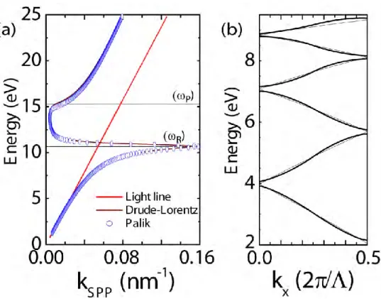
A more rigorous derivation is given in reference [77]. This model explains some metals well such as aluminum and zinc (Figure 2.4a) where as does not for especially some transition metals like silver and gold. (Figure 2.4b) The main reason behind is the interband transitions from the valance orbitals which are just below the Fermi level. Excitation with visible frequencies can cause these transitions. Therefore the upper bound frequency for the surface plasmon polaritons shifts towards red.
Figure 2.4: Dielectric permittivity functions of metals (a) aluminum and (b) silver. The dots are experimental data and the solid lines are calculated using Drude-Lorentz model.
Surface plasmon polaritons are surface bound electromagnetic waves produced by coherent fluctuations of surface charges by the presence of photons [33]. Electric field lines originated at positive charges ends at the negative ones. The parallel components of the electric, E∥, and the magnetic H∥ fields are continuous. Moreover we can assume that the surface charge density at the boundary, ρ=0, since the relaxation time of the electrons is very short compared to the frequency of the electromagnetic field. Therefore we have the continuity of the displacement field D⊥
Since the electric field lines are in opposite direction across the boundary, one should have ε<0 for one of the parts. Metals and highly doped semiconductors satisfy this condition when ω<ωP.
The dispersion relation of the SPPs can be derived using Maxwell’s equations and appropriate boundary conditions. The well known dispersion relation can be calculated by incorporating the continuity of the tangential components of E and H fields and the perpendicular components of D and B fields as
(2.18)
where kSPP is the SPP wavevector and k0=ω/c is the free space wavevector of the
incident photon. A more detailed derivation is presented in [78]. Figure 2.5a shows the calculated dispersion relation on Al/Air interface. There is a bound SPP mode up to ω<ωR (ωR=10.8 eV as predicted by Drude-Lorentz model). The
radiating bulk plasmon modes in the transparency region where ω>ωR can be
explained using free electron model which are beyond the scope of this thesis. The free electron model depicts a natural band gap for ωR<ω<ωP. However the
real metals have the damping factor which sets a maximum for SPP wavevector giving rise to a quasibound leaky mode [78].
If one assumes ε2<|ε1| for the real and imaginary parts of the metal
dielectric function εm, the real and the imaginary parts of the kSPP=k’SPP +i k’’SPP
can be written as
(2.19)
(2.20)
Given that the dielectric constant of the air is 1. Therefore for an air/metal interface the conditions |ε1|>1 and ε1<0 should be met in order to have k’SPP real.
Figure 2.5: Dispersion relation of the SPPs on Al/Air interface. (a) on a smooth surface. (b) on a grating with 300 nm period.
The intensity of the SPP as it propagates along the surface decreased as
exp(-x∙k’’SPP) , x being the propagation direction. The length along which the
intensity drops by 1/e is given as [33]
(2.21)
One other consequence followed by the SPP dispersion relation is that, the SPP line always lies below the light line. That is its momentum is always grater then the light at the same frequency. Therefore the missing momentum must be supplied in order to excite SPPs. Maier reported five mechanisms to excite surface plasmons [78]. They are charged particle impact, prism coupling, grating coupling, the near field excitation and excitation by highly focused optical beam. In this thesis we only used grating coupling. Therefore we will briefly describe the mechanism.
When a grating is fabricated on a flat metal/dielectric interface, the SPP dispersion relation (Equation (2.18)) modifies as follows. The SPP dispersion given in figure 2.5a shifts in reciprocal space by m2π/Λ, where Λ is the period of the grating, and m is an integer. The dispersion curves are than projected to the first Brillion zone. At the crossing sites of the curves, waves interfere and a small band gap opens. The periodicity, depth and the pitch of the grating effects this band gap formation [79]. The modified dispersion relation can be written as
(2.22)
where α is the angle of incidence. The first three SPP modes on Al/air interface with a grating with 300 nm period is illustrated in figure 2.5. Here the band gap openings are sketched. The thin lines under are the actual calculated SPP modes using the equation (2.22). As a consequence of the periodicity in the grating, we now have modes over kx=0. Therefore SPP modes can be excited at normal
incidence.
2.3.2 Localized surface plasmon resonance
The light is scattered by the small metal particles because of the resonant plasma oscillations of the conduction electrons. In the previous chapter we have investigated the surface plasmons which propagate along the metal dielectric surface. In a small particle, on the other hand, there is not enough space for surface plasmons to propagate. Instead there occurs a resonant mode depending on the size and shape of the particle. This resonance is called localized surface plasmon resonance (LSPR). Electric field becomes highly localized in the vicinity of the particle at the resonance frequency. This localization effect can be used in various practical applications as stated in the introduction.
The quantitative analysis of the behavior of metallic nano-particles requires rigorous calculations. Nevertheless, these formulations are limited to basic geometries like spheres. Kuwata et al. developed an analytical model for ellipsoid particles [80] however they establish their model based on
experimental data. Because of analytical limitations, finite difference time domain (FDTD) simulations are often used to predict resonance of a specific nano-particle.
The most basic formulation can be based on assuming the relaxation time within the particle is much shorter than the period of the oscillations. Then one may assume the particle is a spherical object with radius r≪λ, in a uniform electric field. Then, using the appropriate boundary conditions at infinity and the surface of the sphere the polarizability, α, can be calculated as [78]
(2.23)
where ε and εm are the dielectric constants of metal and the surrounding medium, respectively. The most important consequence of this model is that there exist a resonance at re(ε)=-2εm which corresponds to ωP/√3 for Drude like metals. However it does not explain the size dependency of the resonance. Note that this model is only valid for vanishingly small particles.
Mie has established a more general theory to explain the scattering from the gold nano-particles which later called after him as Mie Theory. The polarizability in this theory for larger particles with sizes comparable to the wavelength of excitation can be written as [80, 81]
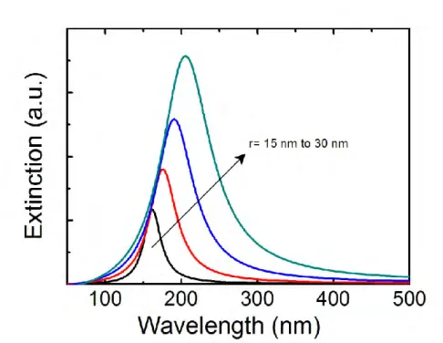
(2.24)
Where V is the volume of the nanoparticle and x=2 , the size parameter. The quadratic term in the numerator explains the retardation effect in excitation of the whole volume of the particle which shifts the resonance. The quadratic term in the denominator shifts the resonance further due to the retardation of the depolarization field. For Drude-like metals this shift in resonance is towards red as particle size increases. The extinction spectra of Al nano-spheres in air as an example is calculated with this model and plotted in figure 2.6.
Figure 2.6: Extinction spectra of Al nano-spheres in air. Curves are calculated using equation (2.24).
20
Chapter 3
Multi-color Sensitive Photodetectors
3.1 Introduction
Light detection is crucial for many technological applications for instance telecommunication, sensing, imaging, temperature monitoring, range measuring, remote control devices and environmental monitoring. A photodetector must somehow convert the electromagnetic energy of the light to a measurable entity. There are mainly three different techniques used for light detection such as photon detectors, thermal detectors and coherent receivers. They all have their own advantage in certain portions of electromagnetic spectrum. In this chapter we worked on UV MSM photodiodes which fall in to the photon detectors category.
The detection of the highly energetic UV light requires wide band gap semiconductors such as AlN, GaN, BN, diamond and SiC [8]. AlN/AlGaN/GaN based UV photodetectors have been widely investigated through past couple of decades [7, 9, 82-87]. Previously, we focused on this particular area, as well. We published a number of articles during that research on various types of photodetectors based on AlGaN material system [15, 19, 20, 23, 88-99]. In this thesis we worked on multi-color sensitive UV photodetectors for further improvement of our previous work.
Detection light in multi-bands has number of advantages over single band. Ability to analyze narrow multi-bands increases the spectral resolution and in some cases spatial resolution as well. Thus the probability of false alarms can be decreased. Current multi band detectors utilize IR/IR [100], UV/IR or UV/visible/IR bands. Multi UV band detectors will further improve the photodetector performance in UV applications such as high temperature sensing, missile plume detection or non-line of sight communication etc.
One method to achieve narrow band detection is the utilization resonant cavity enhancement. Such devices were realized in wavelengths other than UV [101, 102]. The other technique is the usage of highly absorptive filters between the active layers which is rather suitable for AlGaN system. A similar device was reported on a Si photodiode for monitoring laser diodes [103].
We proposed and fabricated multi band photodetectors with and without intermediate filter layers. The capability of detection of different colors on a single chip is the main advantage of these devices. The device can be mounted on a single platform and performs multiple band detection which decreases the size and the cost.
In this chapter we present our work on dual-color and four-color sensing UV photodetectors.
3.2 Dual-Color sensing UV photodetectors
This section was published as “Dual-color ultraviolet metal-semiconductor-metal AlGaN photodetectors” Mutlu Gokkavas, Serkan Bütün, HongBo Yu, Turgut Tut, Bayram Bütün and Ekmel Özbay, Appl. Phys. Lett., 89, 143503 (2006). Reproduced (or 'Reproduced in part') with permission from American Institute of Physics. © 2006 American Institute of Physics.
In this chapter we presented back-illuminated ultraviolet metal-semiconductor-metal photodetectors with two separate spectral responsivity bands on a single AlxGa1−xN heterostructure. This was achieved through epitaxial growth of three AlGaN layers with decreasing Al content. Two of the layers (bottom and top) were the active layers for each band and the one in the middle acts as epitaxial filter. We reached to the bottom layer by recess etching of the top and the filter layer. The top detector has responsivity of 0.12 A/W at 310 nm with 10 V bias and 11 nm full width at half maximum (FWHM), whereas the bottom detector has peak responsivity of 0.1 A/W at 254 nm with 25 V and 22 nm FWHM. Both detectors performed well in terms of dark current with less than 10 fA leakage current.
3.2.1 Concept
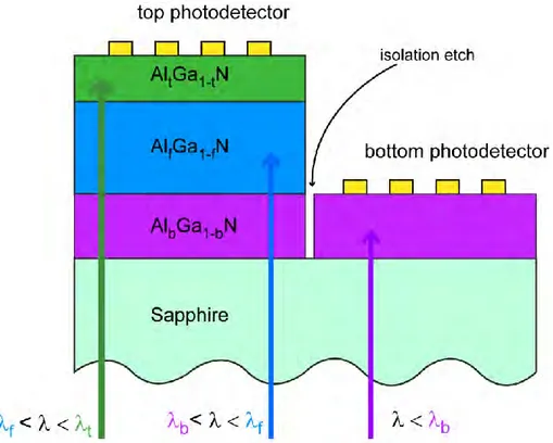
Dual-band MSM photodetector structure consists of three successive layers of epitaxial materials grown on a transparent substrate. The bottom and the top layers are the active layers on which the photodetectors are made. The middle layer blocks light with wavelength below the cut-off wavelength of itself. Thus, it acts as a filter layer for wavelengths below the cut-off.
The growth of AlGaN expitaxial material requires higher temperature as the Al content increases. Therefore growth order should be higher Al content to lower which necessitates the back side illumination of the device. This requirement further simplifies fabrication as it eliminates the deposition of the semi-transparent MSM contacts.
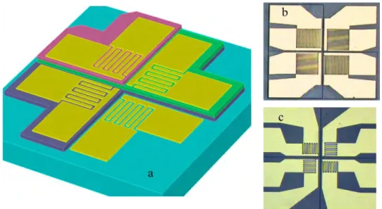
Figure 3.1: Conceptual drawing of the dual color MSM photodetector cross-section.
Figure 3.1 shows the concept of a dual-band photodetector structure. The bottom (violet), middle (blue) and top (green) layers consist of AlGaN layers
with cut-off wavelengths λb, λf and λt. Therefore, only light with, λ > λb can
reach to the middle layer the rest is absorbed in the bottom layer due to the high absorption coefficient. Furthermore, middle absorbs all the light with λ < λf
therefore only light with λf< λ < λt can be absorbed in the top (green) layer. In
the end, blue layer acts as a filter layer to divide the spectrum in half.
3.2.2 Fabrication and Results
We used low-pressure metal organic chemical vapor deposition for the growth of the photodetector structure used in this study. Aixtron AG AIX 200/4 RF-S model reactor, which was installed in Nanotechnology Research Center in Bilkent University, was used for the growth. C-plane double side polished 2 inch diameter sapphire was chosen as substrate is used for AlGaN growth. There are other substrates such as Si and SiC which are widely investigated in AlGaN research but they are not transparent in the range we are interested.
Epitaxial growth was initialized with the typical cleaning process to remove surface contamination. The substrate was annealed at 1100 °C under H2 with flow rate of 3500 sccm at 100 mbar for 10 min. There is a 10% lattice mismatch between the AlN and the sapphire substrate. This causes formation of dislocations and cracks if the material (AlN) is grown directly on the substrate. In order to avoid that, a thin nucleation layer is grown at low temperature with relatively poor crystal quality. The nucleation layer was grown at 550 °C and the thickness was 15 nm. The temperature of the reactor was increased to 1130 °C and the pressure was decreased to 25 mbar after the deposition of the AlN nucleation layer. A 400 nm thick Al0.5Ga0.5N bottom detector active layer was grown at a rate of 2 µm/h. We wanted an abrupt junction between the bottom detector layer and the following 1 µm thick Al0.25Ga0.75N filter layer. Therefore another nucleation layer under the same conditions is grown next. The growth temperature and the pressure of the filter layer were 1080 °C and 50 mbar, respectively. Finally, a 250 nm thick Al0.2Ga0.8N top detector active layer was grown under the same conditions. The composition was changed by altering the
flow rates of the precursors. We did not employ another nucleation layer between the filter and the top detector layers because the composition was not severely different in these layers. No intentional doping was applied during the entire growth process. Trimethylaluminum, trimethylgallium, and ammonia (NH3) were used as reaction precursors for the Al, Ga, and N, respectively. Trimethylaluminum and Trimethylgallium were carried through the bubblers with hydrogen gas.
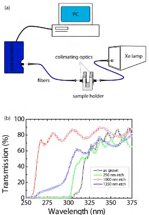
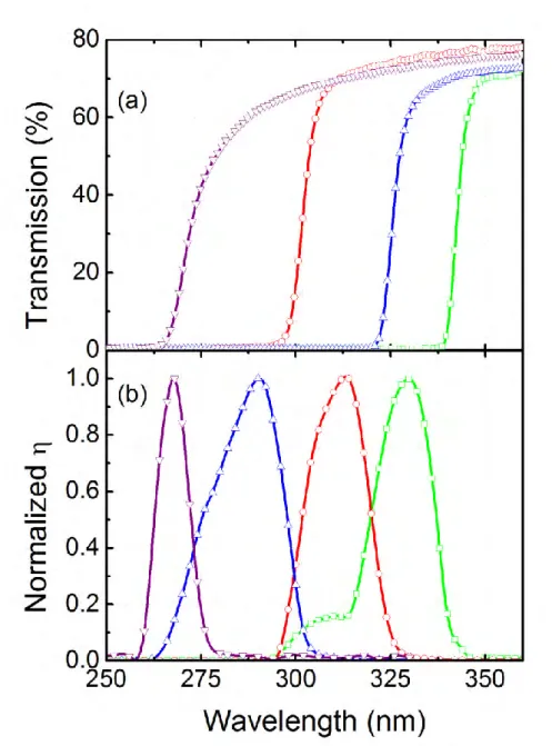
We performed spectral transmission measurements in order to determine the actual Al content and the layer thicknesses of the photodetector structure. Our transmission setup consists of a Xe UV enhanced broad band light source, UV enhanced fiber optic cables, collimating optics mounted on a sample stage and Oceanoptics USB4000 UV enhanced spectrometer. (Figure 3.2a)
Consecutive transmission measurements were performed as we etched the surface. (Figure 3.2b) We used reactive ion etching (RIE) using CCl2F2 plasma with an RF power of 200 W and under 50 µbar pressure. The etch depth was monitored with a profilometer. Figure represents the transmission spectrums of samples of as grown and three subsequent etch depths of 250 nm, 1000 nm and 1250 nm. The sharp cut off at 315 nm of the as grown wafer corresponds to an Al content of 20% which will act as the active layer for the top detector. There remains a slight transmission between 301 and 315 nm which was due to the relatively thin top layer. We observe the shift of the transmission cutoff to 301 nm after the 250 nm etch. This indicates two points: one the top layer is at most 250 nm thick and the Al content of the filter layer is 27%. The transmission cutoff is further shifts to 259 nm when the total etch depth reaches to 1000 nm. We again have about 10% transmission between 259 and 301 nm due to the remaining part of the filter layer on the surface. Finally when we etch down to 1250 nm we observed a sharp cutoff at 259 nm which indicates the Al content of the bottom detector layer is 50%. We further confirm the thickness of the bottom layer by etching 400 nm more. We then have a complete transmission with no cutoff indicating we had reached the sapphire
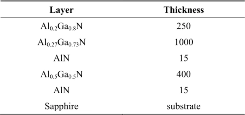
surface. The structure of the wafer is confirmed after these measurements and is summarized in the Table 3.1.
Figure 3.2: Spectral transmission measurements: (a) Schematic diagram of the measurement setup. (b) Spectral transmission measurements of the dual -color photodetector wafer as the recess etch continues.
We cut a 1 × 2 cm2 piece from the wafer. The fabrication started with the recess etching of the top and the filter layers. Firstly, we cover half of the chip with photoresist. Then several RIE steps were performed while monitoring the transmission spectrum each time. Etching continued until the bottom detector
active layer was reached. Cleaning and photoresist coating was applied a number of times since photoresist is etched several times faster than AlGaN. Secondly, MSM contacts were fabricated in a class 100 clean room environment on both etched and unetched part of the chip using UV photolithography. Interdigitated contact distances and widths were varied between 1.5 to 5 µm. We thermally evaporated Ni/Au metal pair (100 Å / 5000 Å) as Schottky contact material. Thirdly, device mesas of 100 × 100 cm2 and 200 × 200 cm2 areas are defined photo-lithographically and etched down to the sapphire via RIE. Finally, the probe pads were fabricated using Ti/Au metal pair (200 Å / 5000 Å). The details of the each fabrication steps are thoroughly covered in appendix A.
Table 3.1: Epitaxial layer content of the dual-color photodetector wafer.
Layer Thickness Al0.2Ga0.8N 250 Al0.27Ga0.73N 1000 AlN 15 Al0.5Ga0.5N 400 AlN 15 Sapphire substrate
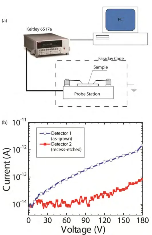
Leakage current characterizations of the photodetectors were made in a class 10000 environment using low noise triaxial cables in a Fraday cage by Keitley 6517A model high resistance electrometer (Figure 3.3a). Devices under test were both 100 × 100 cm2 in area. Contact width and spacing were both 3
µm. Figure 3.3b shows the comparison of measured dark current characteristics of the top and the bottom photodetectors. Both devices exhibited typical characteristics as expected from such wide band gap materials. Dark current at zero bias was 9 fA and 7 fA for top and the bottom photodetectors, respectively. Dark current level does not exceeded 1 pA level for both detectors until such a high bias of 180 V. It is especially better for the bottom detector (more than an order of magnitude lower) which can be attributed to the higher band gap of the bottom layer. There were no sign of breakdown up to 180 V bias. Considering
the aim of this device, having rather wide range of bias voltage is especially an advantage because it is better to operate both of the detectors at about the same responsivity value which is bias dependent. These low levels are a qualitative sign of the low background doping which arises from the dislocations. Therefore it is a clear sign of the high quality of the epitaxial layers. In addition, we may argue that the deep recess etch process did not cause any sort of significant surface damage.
We measured spectral responsivity characteristics of the dual-color photodetectors using a Stanford Research Systems SR830 Lock-in amplifier. The output of the UV enhanced Xe lamp (Spectral Products ASB-XE-175) was monochromated (Spectral Products DK240) then modulated mechanically by a chopper. It is then coupled to a multi-mode non-solarized UV enhances 100 µm diameter fiber which was used to illuminate the photodetector under test (Figure 3.5a) We customized the chuck and the probe holder of the Cascade Probe Station in order to illuminate devices from the back side. (Figure 3.5b and c) We calibrated the spectral output power illumination setup with a NIST-traced calibrated Si photodetector (Newport 818-UV-L). We used 200 × 200 µm2 area and 3 µm contact width and spacing devices for the responsivity measurements.
Responsivity of both photodetectors increased with the applied bias which is typical for MSM devices. Measured responsivity curves in the spectral range of 200 to 500 nm are compared in Figure 3.4. The top photodetector was biased at 10 V whereas the bottom detector was biased at 25 V in order them to exhibit comparable responsivity values. The responsivity of the top photodetector peaked at 310 nm with 0.12 A/W whereas the responsivity of the bottom photodetector peaked at 254 nm with 0.10 A/W. FWHM of the responsivity values are 11 and 22 nm for top and the bottom photodetectors, respectively.
Figure 3.3:IV characterization of the dual color photodetectors (a) Schematic diagram of the leakage current characterization setup. (b) Dark current measurements of the top and bottom photodetectors.
Figure 3.4: Spectral responsivity measurements of the dual-color photodetectors.
There is a quite large rejection (about four orders of magnitude) in terms of responsivity for both bands. The responsivity of the top photodetector drops very sharply below 300 nm which is due to 1 µm thick the Al0.27Ga0.73N filter layer. There is a good agreement if we compare this to the spectral transmission measurements (Figure 3.2b) prior to the fabrication. The filter layer blocks the light with wavelength below 300 nm which explains the sharp drop in the responsivity curve of the top photodetector. The increase towards the shorter wavelengths is not the real increase in the response of the device but the decrease in the dynamic range of our measurement setup. That is, the measured photocurrent remains constant at the lowest possible measurable value whereas the optical power of the illumination decreases. Hence, the responsivity seems increasing as the wavelength decreases. On the other hand, the responsivity of the bottom photodetector drops fairly sharp above 260 nm which is due to the band gap of the active bottom layer. Slight response between 300 to 400 nm of the bottom photodetector is due to the low energy (compared to band gap) trap
states originated from the imperfections such as dislocation and impurities which are much like the phenomenon so called yellow luminescence in GaN The minor increase towards the 500 nm is because of higher order leakage of the monochromator. As a result, top photodetector rejects to bottom band more than four orders of magnitude while the bottom photodetector rejects the top band more than three orders of magnitude. In addition, both photodetectors rejects visible by more than four orders of magnitude at 500 nm.
3.2.3 Conclusion
We fabricated and characterized dual-color back illuminated UV MSM photodetectors with separate spectral bands monolithically on the same chip. This was achieved by growth of three different Al content epitaxial layers. Top and the bottom layers were used as an active absorption layer while the middle layer was used as passive absorptive filter layer. The bottom layer was reached via recess etching of the top and the middle layers. The peak response of the top photodetector was 0.12 A/W at 310 nm with 10 V bias whereas the peak response of the bottom photodetector was 0.10 A/W at 254 nm with 25 V bias. FWHM of the top and bottom photodetectors were 11 and 22 nm respectively. Top photodetector rejected the light in the bottom photodetector operation band with more than four orders of magnitude, and bottom photodetector rejected light in the top photodetector operation band with more than three orders of magnitude. Both photodetectors exhibit superior dark current characteristics with no more than 1 pA up to 180 V bias. Given the ozone layer absorption at 280 nm, we can conclude that bottom photodetector is solar blind while the top photodetector is visible blind. This property gives a unique ability to monitor UV radiation differently by day and night to the overall device.
Figure 3.5: Schematic diagram of the spectral photoconductivity setup (a). The original (b) and the custom made brass (c) chucks are presented in the photographs. Sample is placed over the hole on the bracket. The fiber probe is then aligned from the bottom.
3.3 Four-Color sensing UV photodetectors
This section along with the section 3.4 was submitted as “Four-color ultraviolet metal-semiconductor-metal AlGaN photodetectors” Mutlu Gokkavas, Serkan Bütün, Wlodek Strupinski and Ekmel Özbay, Semicond. Sci. Tech. October, 2011.
Ultraviolet (UV) light sensitive devices are fabricated on AlGaN templates grown on c-plane sapphire by metal-organic chemical vapor deposition. We fabricated back illuminated metal-semiconductor-metal (MSM) photodiodes with multiple color sensitivity on single epitaxial structure. Our devices consist of several active layers which are sensitive to different portions of the UV spectrum. We incorporated the self filtering effect of the epitaxially thick (around 1 um) active layers in order to suppress the other part of the spectrum. We fabricated 4 separate MSM diodes on 4 different active layers by recess etching of the surface. The resultant device showed well separated four peaks at 267, 290, 309 and 328 nm with FWHM of 9, 22, 17 and 18 nm respectively. The leakage current of the devices were on the order of 10 pA.
3.3.1 Concept
Four-color AlGaN photodetectors consists of four active layers with different Al content. We include a fifth passive filter layer down at the bottom as well in order to make fourth band further narrower after our first attempt. A conceptual drawing of a four color sensing device is shown in Figure 3.6. Different epitaxial AlGaN layers with different Al concentrations are represented with different colors. Each epitaxial layer has a separate MSM photodetector structure fabricated on. The thicknesses of each active epitaxial layer are sufficient enough to absorb all the light below its band gap. Therefore each acts as a filter layer for the photodetector on the layer above it.
3.3.2 Fabrication and Results
The epitaxial growth of AlxGax-1N layers with different Al content on one another is the main challenge in this work. We designed our structure such that the Al concentration of the epitaxial layers is decreasing along the growth direction because it is nearly impossible to grow otherwise. Hence, the back illumination is used.