Electro-optic and electro-absorption
characterization of
InAs quantum dot waveguides
Imran B. Akca, 1,* Aykutlu Dâna,1 Atilla Aydinli,1Marco Rossetti,2 Lianhe Li,2Andrea Fiore,2 and Nadir Dagli3
1Materials Science and Nanotechnology Program, Physics Department, Bilkent University, 06800,
Ankara, Turkey
2Institute of Quantum Electronics and Photonics, Ecole Polytechnique Fédérale de Lausanne EPFL,
CH-1015 Lausanne, Switzerland
3ECE Department, University of California, Santa Barbara, CA-93106, USA *Corresponding author: [email protected]
Abstract: Optical properties of multilayer InAs quantum dot waveguides, grown by molecular beam epitaxy, have been studied under applied electric field. Fabry-Perot measurements at 1515 nm on InAs/GaAs quantum dot structures yield a significantly enhanced linear electro-optic efficiency compared to bulk GaAs. Electro-absorption measurements at 1300 nm showed increased absorption with applied field accompanied with red shift of the spectra. Spectral shifts of up to 21% under 18 Volt bias was observed at 1320 nm.
©2008 Optical Society of America
OCIS codes: (230.4110) Modulators; (250.7360) Waveguide modulators.
References and links
1. R. B. Welstand, S. A. Pappert, C. K. Sun, J. T. Zhu, Y. Z. Liu, and P. K. L. Yu, “Dual-function electroabsorption waveguide modulator/detector for optoelectronic transceiver applications,” IEEE Photon. Technol. Lett. 8, 1540–1542 (1996).
2. L. Lembo, F. Alvares, D. Lo, C. Tu, P. Wisseman, C. Zmudzinski, and J. Brock, “Optical electroabsorption modulators for wideband, linear, low-insertion loss photonic links,” Proc. SPIE Photon. Device Eng. Dual-Use Appl. 2481, 185–196 (1995).
3. S. S. Lee, R. V. Ramaswamy, and V. S. Sundaram, “Analysis and design of high-speed high-efficiency GaAs-AlGaAs double-heterostructure waveguide phase modulator,” IEEE J. Quantum Electron. 27, 726 (1991).
4. D. A. B. Miller, D. S. Chemla, T. C. Damer, A. C. Gossard, W. Weigmann, T. H. Wood, and C. A. Burrus, “Band-Edge Electroabsorption in Quantum Well Structures: The Quantum-Confined Stark Effect,” Phys. Rev. Lett. 53, 2173 (1984).
5. S. Schmitt-Rink, D. A. B. Miller, and D. S. Chemla, “Theory of the linear and nonlinear optical properties of semiconductor microcrystallites,” Phys. Rev. B 35, 8113 (1987).
6. K. Shimomura, S. Arai, and Y. Suematsu, “Operational wavelength range of GaInAs(P)-lnP intersectional optical switch using fieldinduced electrooptic effect in low-dimensional quantum-well structures,’’ IEEE J. Quantum Electron. 28, 471-478( 1992).
7. L. Davis, K. K. Ko, W.-Q. Li, H. C. Sun, Y. Lam, T. Brock, S. W. Pang, and P. Bhattacharya, “Photoluminescence and electro-optic properties of small (25–35 nm diameter) quantum boxes,” Appl. Phys. Lett. 62, 2766 (1993).
8. O. Qasaimeh, K. Kamath, P. Bhattacharya, and J. Phillips, “Linear and quadratic electro-optic coefficients of self-organized In0.4Ga0.6As/GaAs quantum dots,” Appl. Phys. Lett. 72, 1275 (1998).
9. S. Ghosh, A.S Lenihan, M.V.G Dutt, O Qasaimeh, D.G Steel, and P. Bhattacharya, “Nonlinear optical and electro-optic properties of InAs/GaAs self-organized quantum dots,” J. Vac. Sci. Technol. B 19, 1455–1458 (2001).
10. J. Tatebayashi, R.B. Laghumavarapu, N. Nuntawong, and D.L. Huffaker, “Measurement of electro-optic coefficients of 1.3 μm self-assembled InAs/GaAs quantum dots,” Electron. Lett. 43, 410-412 (2007). 11. G. Moreau, A. Martinez, D.Y. Cong, K. Merghem, A. Miard, A. Lemaître, P. Voisin, A. Ramdane I.
Krestnikov, A. R. Kovsh M. Fischer, and J. Koeth, “Enhanced In(Ga)As/GaAs quantum dot based electro-optic modulation at 1.55 µ m,” Appl. Phys. Lett. 91, 91118 (2007).
12. A. Markus, J. X. Chen, C. Paranthoen, A. Fiore, C. Platz, and O. Gauthier-Lafaye, “Simultaneous two-state lasing in quantum-dot lasers,” Appl. Phys. Lett. 82, 1818 (2003).
13. S. Nishimura, H. Inoue, H. Sano, and K. Ishida, “Electrooptic Effects in an InGaAs/InAlAs Multiquantum Well Structure,” IEEE Photon. Technol. Lett. 4, 10 (1992).
1. Introduction
Nonlinear optical and linear electro-optic materials find use in switching and modulation devices for photonic integrated circuits. For modulators in telecommunications small size and modulation voltages are desired. Both electro-absorption (EA) and electro-optic (EO) modulators are candidates for use in external modulation links in telecommunications. These modulators can be realized using either bulk semiconductor materials [1] or materials with multiple quantum dots or wells [2].
Much has been done to realize both EO and EA modulators in quantum wells using both Franz-Keldysh and quantum confined Stark effects (QCSE). Quantum wells demonstrate enhanced electro-optic effects due to the built-in birefringence and a quadratic electro-optic (Kerr) effect arising from the quantum confined Stark effect (QCSE) near the excitonic absorption edge [3,4]. Recently, advances in crystal growth have triggered the study of self organized quantum dots. Quantum dots are expected to exhibit enhanced optical nonlinearities and enhanced electro-optic effects due to the modification in their density of states since the ratio of optical nonlinearity of a quantum dot layer to that of a bulk material is proportional to aB3/V where aB is the Bohr radius and V is the volume of the quantum dots [5,6]. Since both EA and EO modulators require small size and low modulation voltages, possibility of obtaining quantum dots with enhanced electro-optic and/or electro-absorption coefficients makes them attractive for such applications.
In the literature there is limited data on EO and EA effects in quantum dots. Furthermore, little has been reported on the voltage dependent modulation of quantum dot embedded waveguides [7-9]. Davis et.al. have measured the electro-optic coefficient of lithographically defined In0.15Ga0.85As quantum boxes embedded in optical waveguides at 1.15 μm using the phase retardation technique [7]. They found increased electro-optic coefficient when compared with GaAs. Using the phase retardation technique, Q. Qasaimeh et.al. and Ghosh et.al. measured both linear and quadratic electro-optic coefficients at 1.15 μm of self organized In0.40Ga0.60As quantum dots and have also observed enhanced electro-optic coefficients [8,9]. Using the same approach, electro-optic coefficients of self assembled InAs and In(Ga)As quantum dots were recently measured and enhanced electro-optic coefficients were reported [10,11].
In this article, we report on the measurements of both EO and EA properties of multilayer InAs/GaAs self-organized quantum dots. We use the transmission through Fabry-Perot resonators formed by two cleaved facets in waveguides at wavelengths of 1300 nm and 1500 nm to determine the absorption properties of quantum dots in addition to electro-optical properties. This is in contrast with previous work, where phase retardation method was exclusively used.
2. Samples
We worked on waveguide structures containing three layers of quantum dots (3QDs) of lengths in the range of 1-1.6 mm. These structures were grown by molecular beam epitaxy to be used as quantum dot lasers. The active region is formed by three layers of self-assembled InAs QDs, which are covered by a 5-nm In0.15Ga0.85As QW and separated from each other by a 40-nm GaAs spacer layer. The areal dot density of our lens-shaped QDs is 3x1010 cm-2. The laser cavity is clad by 1.55 μm of Al0.7Ga0.3As, which is n-doped on the substrate side and p-doped on the top side. Our devices are single mode ridge waveguide structures with varying
oxidized layers is further improved by deposition of a 250 nm thick Si3N4 layer. This layer ensures a minimal current leakage through the large metal bond-pads used for the p-contacts. The p-contact (Ti/Pt/Au) is realized by thermal evaporation and lift-off. After p-contact deposition the substrate is thinned down to 200 µm and then the n-contact (Ni/Ge/Au/Ni/Au) is deposited uniformly on the sample substrate side. Finally, the desired cavity lengths are obtained by cleaving. For each sample lasing is peaked at nearly 1285 nm [12]. Detailed structure is given in Fig. 1.
Fig. 1. Detailed structure of the samples used in the measurements. Al0.7Ga0.3As layers at the GaAs interfaces are graded.
3. Measurements and results
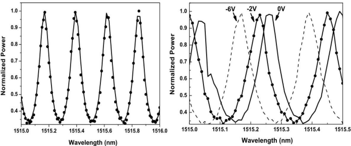
Measurement of the electro-optic coefficients at 1515 nmwas carried out by coupling a TE polarized light from a tunable laser (Santec Tunable LD Light Source TSL-520)onto one end of the waveguide with a lens shaped fiber. A DC voltage source was used to apply 0 to 20 Volt reverse bias to the samples. The applied electric field was perpendicular to the quantum dot layers. At each voltage level, the transmission through the device was recorded as a function of wavelength and voltage. Experimental results are given in Fig. 2. Fabry-Perot resonances with large contrast were obtained and experimental data fitted well with the theoretical formula. The well known Fabry-Perot transmission equation is used in fitting to the measured data and the fitting parameters were mode effective index, loss coefficients and a voltage independent phase factor. The effective mode index was then calculated based on this curve fitting.
Fig. 2. (a) Fabry-Perot resonances at 1515 nm for 6 Volt reverse bias. The dots show the experimental data and the line indicates the optimum curve fit. (b) Voltage dependent shift of Fabry-Perot resonances. Significant tuning is observed with relatively low voltages.
No voltage-dependent spectral shift is observed for TM polarization. This indicates that the quadratic electro-optic coefficient is not effective at this wavelength and that the linear electro-optic coefficient is dominated by the r41 component, similar to bulk. The linear electro-optic coefficient responsible for modulation is obtained using the mode effective index difference between two specific voltages. The change in refractive index as a function of applied voltage is extracted from the data in Fig. 2(b) and is shown in Fig. 3.
Fig. 3. Variation in refractive index as a function of applied voltage at 1515 nm. The dots show the experimental data and the line indicates the linear fit.
The change in mode effective index varies linearly with the applied voltage and the maximum change is 2x10⁻⁴ for 6 Volt bias at 1515 nm. The change in the mode effective index due to applied voltage (Δn(V) ) is given in below [13] and describes the data in Fig. 3 quite well:
mode effective index, V is the applied voltage and Γ is the overlap of the vertical electric field component with the optical mode. Since they are very thin, the overlap of quantum dots with the optical mode is very small. Such a small value is hard to calculate accurately. Therefore we calculated the modal electro-optic coefficient, for the entire layer subjected to the electric field. This layer includes both the quantum dots and the bulk GaAs adjacent to quantum dots. In this calculation, we assumed that Γ remained unchanged from a waveguide in which quantum dot layers are replaced by bulk GaAs. This way we obtained an effective electro-optic coefficient which is about 20% higher than that of bulk GaAs. As a matter of fact, examination of Fig. 2 (b) reveals that full on/off modulation is possible using only 6 V. This corresponds to less than 1 V-cm modulation efficiency. In other words, using this modulator as the arms of a push pull driven Mach-Zehnder modulator, less than 1 V drive voltage would result for 1 cm long arms. In simulations when quantum dot layers are replaced with a bulk GaAs layer on/off modulation voltage is obtained as 7.27 V which indicates more efficient modulation in the quantum dot sample. It should be noted that in this analysis Γ is the only calculated quantity. The observed improvement in the effective electro-optic coefficient could not be due to the difference in Γ between waveguides with GaAs core and waveguides with quantum dot cores. Although index of quantum dot layers is higher than GaAs, they only perturb the waveguide mode slightly due to their very small overlap with the optical mode. The overlap factor of InAs quantum dot layers is calculated using finite difference beam propagation method simulations and is approximately 0.015 for all samples. To get a 20% improvement in modulation efficiency due to Γ alone would require unrealistically high index for the quantum dot layers. In order to generate a 20% improvement in the overall modulation efficiency the electro-optic coefficient of the quantum dot layers itself should have improved significantly. Using the QD overlap factor quoted above we estimate that for the QD layer
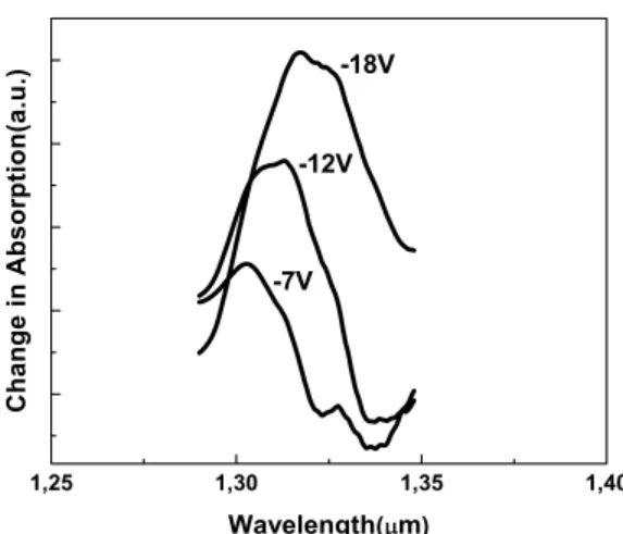
n3r41 term is about 7-10 times higher than bulk GaAs. This is a very significant improvement. Electro-absorption measurements were also conducted at 1300 nm by coupling light from a tunable laser (Santec TSL-320 for 1300 nm) onto one end of the waveguide with a lens shaped fiber. Reverse bias voltage (0-20 V) was applied using a DC voltage source. A wide wavelength range was scanned and at each voltage level, the transmission through the device is recorded as a function of wavelength. The electro-absorption coefficients are obtained using: 21 10 log 1 T K r K α = ⎛⎜⎜ + ⎞⎟⎟ − ⎝ ⎠ (2)
where K=Tmin/Tmax, r2=[(ne-1)/(ne+1)]2 is the facet reflectivity and, ne is the mode effective index. Since the structure lases at 1285 nm, absorption near 1300 nm is expected. High absorption values at 1309 nm were obtained as expected. Indeed, at 1515 nm, the average insertion loss is 3.1 dB/cm for all samples and at 1309 nm this value increases to 30 dB/cm. Considering that all other factors remain the same, the increase in insertion loss by a factor of 10 is indicative of excitonic absorption. The absorption spectrum of the samples was also studied under applied electric field. Absorption spectra of all samples shift to lower photon energies with increasing electric field. Maximum change of absorption was observed at 1.32
Fig. 4. Change in absorption due to applied reverse bias. Red shift of the spectra should be noted with increasing applied voltage.
4. Conclusions
In conclusion, the low voltage modulation in InAs quantum dot waveguides was observed. The electro-optic coefficients of multilayer quantum dot structures far away from the lasing wavelength were measured. The linear electro-optic coefficient of InAs QDs is found to be significantly larger than that of GaAs bulk material. The electro-absorption of these multilayer quantum dot waveguides at 1300 nm was also measured. Since these structures were designed as lasers, large absorption near the lasing wavelength (1285nm) was obtained as expected. Absorption edges of the samples shifted to lower photon energies with increasing electric field. Change in absorption spectra as high as 21% was observed at 1.32 μm at 18 Volt bias. These results are promising for QD-based electro-optic and electro-absorption modulators. Acknowledgement
This project is supported by Turkish Scientific and Technical Research Council (TUBITAK); Grant No: 103T115.