PROCEEDINGS OF SPIE
SPIEDigitalLibrary.org/conference-proceedings-of-spieHigh-speed high-efficiency
resonant-cavity-enhanced photodiodes
Ekmel Ozbay, Ibrahim Kimukin, Necmi Biyikli, Orhan
Aytur, Mutlu Goekkavas, et al.
Invited Paper
High-Speed
High-Efficiency Resonant Cavity Enhanced Photodiodes
Ekmel Ozbay, Ibrahim Kimukina, Necmi Biyik1i' and Orhan Ayturb,
Mutlu Gökkavas', GOkhan Uluc, and M. Selim Un1U'Richard P. Mirinc, Kris A. Bertness", and David H. Christensend Elias Towee, and Gary Tuttli
aDepament ofPhysics, Bilkent University, Ankara, Turkey 06533
bDt
ofElectrical
and Electronics Engineering, Bilkent University, Ankara, Turkey 06533
of
Electrical and Computer Engineering, Boston University, Boston MA 02215
öptoe1ectronics Division, National Institute of Standards and Technology, Boulder CO 80303
eDepament of Electrical Engineering, University of Virginia, Charlottesville, VA 2933
"Department of Electrical and Computer Engineering and Microelectronics Research Center, Iowa State
University, Ames, IA 50011
ABSTRACT
In this paper, we review our research efforts on RCE high-speed high-efficiency p-i-n and Schottky photodiodes. Using a
microwave compatible planar fabrication process, we have designed and fabricated GaAs based RCE photodiodes. For RCE Schottky photodiodes, we have achieved a peak quantum efficiency of 50% along with a 3-dB bandwidth of 100 GHz. The tunability of the detectors via a recess etch is also demonstrated. For p-i-n type photodiodes, we have fabricated and tested widely tunable devices with near 100% quantum efficiencies, along with a 3-dB bandwidth of 50 GHz. Both of these results correspond to the fastest RCE photodetectors published in scientific literature.
Keywords: high speed photodetectors, resonant cavity enhancement, Schottky diode, p-i-n photodiode, quantum efficiency
1. INTRODUCTION
As the information revolution continues at an increasing pace, there is an exponentially increasing demand for larger telecommunication bandwidths. The optical communication systems are currently the only viable solution for this bandwidth demand. Optoelectronic components such as semiconductor lasers, photodetectors, modulators, and optical
amplifiers are at the heart of these communication systems, and the performance of all these devices should be increased to
meet the existing and expected bandwidth requirements. Besides the optical communication systems, high-performance photodetectors are also vital components of optical measurement systems.' Both Schottky photodiodes,24 and p-i-n
photodiodes,5'6 offer high-speed performance to fulfill the needs of such systems. However, the efficiency of these detectors has been typically limited to less than 10%, mostly due to the thin absorption region needed for short transit times. One can
increase the absorption region thickness to achieve higher efficiencies, but this also means longer transit times that will
degrade the high-speed performance of the devices. Resonant cavity enhanced (RCE) photodetectors offer the possibility of
overcoming this limitation in the bandwidth-efficiency product of conventional photodetectors.79 High-speed RCE photodetector research has mainly concentrated on using p-i-n photodiodes'° and avalanche photodiodes, where 75% quantum efficiency along with a >20 GHz bandwidth" ,and 3 dB bandwidths as high as 33 GHz'2 have been reported.
Recently, we have fabricated RCE Schottky photodiodes with 50% quantum efficiency and a 50 GHz frequency
performance.'3'4 We have also achieved -.100 GHz performance, along with a 20% quantum efficiency.'5 Our work pin
type RCE photodiodes resulted in >90% quantum efficiency along with a 50 GHz performance.'6 In this paper, we review our recent work on design, fabrication, and testing of widely tunable, high-speed RCE photodiodes for operation at 800-900 nm.
ti
—d-'---
t2
E
r2e12
Figure 1. Schematics of the Fabry Perot cavity model. The shaded absorption region was used to simulate the active region placed in the cavity.
2.
THEORY
OF RESONANT CAVITY ENHANCEMENT IN PHOTODETECTORSThe well-known bandwidth-efficiency trade-off is a major blockade for using high-speed photodiodes in long-haul telecommunications. As the active region thickness is decreased to minimize the transit time for high-speed purposes, the quantum efficiency of the same device proportionally decreases. For a photodiode with transit-time limited frequency
response, the 3-dB bandwidth can be formulated as
V
f3dB 0.45—
d
(1)where v is the drift velocity of the charge carrier, and d is the active region thickness. For thin active regions, the absorption
can be formulated as
= (1— R)(1 —e
ad) (1— R)cxd
(2) where x is the power absorption loss factor of the optical field within the active region, and ad <<1 is assumed. Using equations 1 and 2, the bandwidth-efficiency product can be obtained as,which is independent of the active region thickness.
f3dB
=
0.45(1 — R)va (3)This bandwidth-efficiency trade-off can be solved by placing the active region in a Fabry-Perot cavity (Figurel). This is
usually achieved by integrating the photoactive region with a bottom Bragg mirror. In a Fabry-Perot cavity, the optical field
is enhanced resulting in increased efficiencies. The electric field component for the forward traveling wave Ef inside the
cavity (Figure 1) can be related to the incident field E as:
tl 1;,
1
',
where r1e and r2e are the reflection coefficients of the mirrors, t1 is the transmission coefficient of the front mirror, 3 is the propagation constant for the traveling EM wave in air, and L is the total width of the cavity. The backward traveling
wave Eb is related to Ef as:
Eb =r2e_ade_J42)Ef.
(5)UsingEqs. (4) and (5),wecan calculate the power enhancement factor T, which is defined as the ratio of the absorbed
power inside the absorption layer, to the power of the incident EM wave,
E
(4)—
(1+R2e)(1—R1)
—1—2R1R2
e cos(2 + Ø
+
02) +R1R2e
(6)where R1 =r12and R2 =r22,arethereflectivities of the mirrors of the cavity. The above result is normalized with respect to
the incident field absorbed by the detector in the absence of the cavity.
As can be seen from Equation 6, the introduction of a Fabry-Perot cavity can increase the quantum efficiency without effecting the high-speed properties. Besides, the detector becomes wavelength selective which may be very useful for wavelength division multiplexing (WDM) based optical communication systems.
3. RCE SCHOTTKY PHOTODIODES
3.1 DESIGN AND FABRICATION
We used an S-matrix method to design the epilayer structure of the RCE Schottky photodiodes. The structure was
optimized for top-illumination and it consisted of a bottom Bragg mirror integrated with a Schottky diode structure. The mirror was formed by 15 pair AlAs(755 A)/GaAs(637 A) quarter wave stack designed to operate at 900 nm. The Schottky diode region had a 0.630 m thick N (ND =3x10181/cm3) layer for ohmic contacts, and a 0.3 jim thick N (ND =1.2 x 10"
1 1cm3) region for the generation and transport of photogenerated carriers. The N region consisted of a 1 300 A thick photoactive 1n008Ga092As region, sandwiched between two GaAs N layers. The top GaAs N layer between the Schottky metal and the 1n008Ga092As region had a thickness of 500 A, while the other N region had a thickness of 1200 A. The
photoactive In008Ga92As region was placed closer to the metal contact in order to equalize the transit times of
photogenerated electrons and holes. The In008Ga092As/GaAs interfaces were graded to avoid hole-trapping. The total length of the cavity was designed to get the resonance to occur at 900 nm.
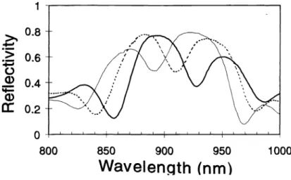
The epitaxial layers are grown by a solid-source MBE on semi-insulating GaAs substrates. The epitaxial design of the structure permits wavelength tuning by a recess etch of the top GaAs layer. Figure 2 shows the spectral reflectivity
characteristics of the epitaxial wafer for different recess etches. As can be shown from the plot, the resonant wavelength can be tuned from 930 nm to 890 nm, by a 600 Angstrom recess etch.
1
.?
0.6
C,0.4
a)
a: 0.2
0
800
1000Wavelenqth
(nm
Figure2. Reflectivities of the samples with different recess etches. The thick solid line refers to as grown sample, the dashed line refers to 300 Angstrom recess etched sample, and the thin solid line refers to the sample with a 600 Angstrom
recess etch.
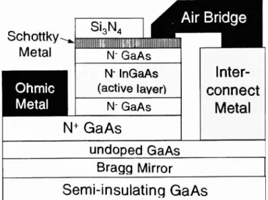
Figure 2.Microphotograph ol thc tahiicated RCF photodiode.
Semi-insulating GaAs
Figure 3. Diagram showing the Crosssection ofa lihricated RCE Schottkv photodiode.
We lahrieated the epitaxial wafers using a monolithic microwave—compatible tahrication Aiinci opliotograph ol the tabricatedphotodiodesis shown in Figure 2. First, ohmic contacts to the N+ layers were loritied by a recess etch through the
0.3micron N Liver. This
was tolloed h
asell—aligned Au—( c—Ni liltolT and a rapid thermal anneal. The senu—transparent Schottkvcontact as hrmcd bydeposition of 200A Au. Using an isolation mask. wc etched awa\ all ol the epilaversexcept the active areas. Then, we evaporated Ti/Au interconnect metal which tormcd coplanar waveguide (CPW)
transmission lines oh topof the semi—insulating substrate. Thenextstep wasthe deposition and patterningol a 2000Athick
silicon nitride layer. The thickness of the nitride layer was chosen to act as an antireflection coating loi the RCF Schottky
photodiode at the design wavelength. Besides passivation and protection of the surlace. the nitride was also used as the
dielectric ol the metal—insulator—rnetal bias capacitors. Finally. I .5 micron thick Au layer was used as an airbridge to connect
the center of the CPW to the top Schottky metal. A cross—section oh the fabricated photodiodes is shown in Figure 3. The resulting Scbottkv diodes had breakdown voltages larger than 12 V. The dark-current of a I 50x ISO pin device at IV bias was 3(1 nA. Using the forward current—voltage characteristics, we measured the harrier height of the Schottkv unctmon to be 0.f3 eV. I
Si3N4
Schottky
Metal
N- GaAsOhmic
Metal
N- lnGaAsInter-(active laver
connect
N- GaAs
Metal
N GaAs
undoped GaAs
>
0
C
0
Iio.i
E
C
cø0
>
0
C
0
w
E
C
0
Wavelenqth (nm)
0.2
0
800
850
900
950
Wavelenqth (nm
850
900
0.8
0.6
0.4
0.2
0
800
950
Figure4. (a) Measured photoresponse of the RCE Schottky photodiode. (b) Simulated photoresponse of the same structure.
2.2 MEASUREMENTS
Photo response measurements were carried out in 700-900 nm wavelength range, by using a tungsten-halogen projection lamp as the light source, a single pass monochromator, a mechanical chopper, and a lock-in amplifier. Output of the monochromator was coupled to a multimode fiber. The monochromatic light was delivered to the devices by a lightwave fiber probe, and the electrical characterization was carried out on a probe station. The incident power spectrum was
measured by a calibrated optical powermeter.
For spectral photoresponse measurements, we used a tungsten lamp source with a 1/3 meter grating monochromator. The
monochromatic light was delivered to the devices by a multimode fiber and the electrical characterization was carried out on
a probe station. The spectral response was corrected by measuring the light intensity at the fiber output by a calibrated optical power meter. Overall error is expected to be within several percent. For photospectral measurements, we used a 150150 im photodiode biased at -2.0 Volts.
15
1o
c
O
>
-5100
Time (psec)
Figure5.Pulseresponse of RCE Schottky photodiode.
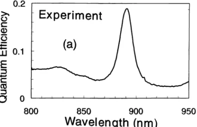
The photoresponse of the device obtained by using the aforementioned set up is shown in Figure 4(a). For comparison purposes, the simulated quantum efficiency of the epitaxial structure is shown in Figure 4(b). There is a reasonable agreement between the calculated and the measured spectral responses. The resonant wavelength of the device is 895nm,
which is very close to the design wavelength of 900 nm. When compared with a single-pass structure, the enhancement
factor of the device is in excess of 6 at the resonant wavelength. The full-width at half maximum was 1 5nm,corresponding
to a —1 .6% spectral width. Although we predicted a peak quantum efficiency of 70%, the measured peak quantum efficiency
was around 1 8%. The discrepancy between the experiment and simulation is due to the shift of the Bragg mirror center
wavelength during the MBE growth, which resulted in a 60% bottom minor at 900 nm.
High-speed measurements were made with short optical pulses of 1 .2 ps FWHM at 895nmwavelength. The optical pulses
from the laser were coupled into a single-mode fiber, and the other end of the fiber was brought in close proximity of the photodiode by means of a probe station. We used a 8x9 im device biased at -2 Volts, and the photodiode output was measured by a 50GHzsampling scope. Figure 5showsthe measured photodiode output which had a FWI-IM of 10 psec.
There is no residual photocurrent after the pulse fall-time (except the smaller bumps due to reflections from the electrical contacts) which indicates that there is no diffusion component which may limit the bandwidth of the device. This is in accordance with our expectations, as the photoactive region is totally depleted, and the other regions are transparent at the
resonant wavelength.7 The measurement is limited by the experimental set-up. The pulsewidth of the 50GHzscope,tscope 5
specified as 9.0 psec with an optimized Gaussian response. The optical pulse can also be assumed as a Gaussian pulse with
a pulsewidth, toptical, of 1 .2 psec pulsewidth. The measured pulsewidth tmeas canthen approximated as:'7
I 2 7 2
'rmeas \I'rdevice + '1scope 'roptcai . (7)
This is very accurate for Gaussian pulses and a good approximation for actual measurements. Using the above numbers in Eq. 7, the device speed is estimated to be around 4 psec. As our experimental result is very close to the measurement limit of the 50GHzscope, we do expect a large uncertainty in this speed estimation. However, this estimated value (obtained from the experiment) value is in good agreement with our predicted device speeds. The device has an RC time constant of 1.4 psec, and the equalized electron and hole transit times are around 3.5psec. The total speed of the device is then
estimated to be 3.8 psec, which is very close to the value we obtain from Eq. 7.
303
I 00
>% 80
C.)60
w 40
20
750
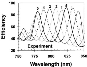
Figure6. Experimental photoresponse characteristics of fabricated devices. Plot 1 corresponds to the as-grown sample, while plots 2-5 correspond to the characteristics after consecutive recess etches.
3.
PIN
PHOTODIODESAs mentioned earlier, p-i-n photodiodes are also widely used in telecommunication systems. The details of the p-i-n photodiode epitaxial structure we have used in this work is given in Ref. 16. In this structure, the bottom Bragg mirror is made of quarter-wave stacks (A10,20Ga08oAs/A1As) designed for high reflectance at 820 nm center wavelength. Carrier
trapping was avoided by using linear composition grading at interfaces of the absorbing layer. The active layer thickness, d, was chosen such that the maximum quantum efficiency is obtained by,
R1 =R2e2"
(8)where a is the absorption coefficient, R1 is the top air-semiconductor mirror reflectance, and R2 is the bottom Bragg minor
reflectance [7]. The reflectivity measurements are used to investigate the epitaxial structure of the wafer. The resonance occurs at 826 nm with a measured reflectance minimum of 5%, while our theoretical simulations predict nearly zero
reflectance at the same wavelength. The measured resonance wavelength changes from 826 nm at the center of the wafer, to
8 1 6 nm at the edge of the wafer. This epilayer thickness variation across the wafer and small deviations between growth
and design explain the difference between the theoretical and experimental reflectance characteristics.
The samples were fabricated by a microwave-compatible process similar to the one used for the Schottky photodiodes. The
p+ ohmic contact was achieved by an Au/Ti liftoff. The n and ohmic contacts were then achieved by a rapid thermal anneal at 450°Cfor 25 seconds. The resulting p-i-n photodiodes had breakdown voltages greater than 14 V. The dark
current of a 30 im diameter circular device at —1 V bias was 20 pA.
Photoresponse measurements were carried out in the 750-850 nm wavelength range by using a tungsten-halogen projection
lamp as the light source and a single pass monochromator. The output of the monochromator was coupled to a multimode
fiber. The monochromatic light was delivered to the devices by a lightwave fiber probe, and the electrical characterization
was carried out on a probe station. The spectral response was measured using a calibrated optical powermeter. For photospectral measurement, large area photodiodes (250 im x 250 rim) were chosen to ensure all of the optical power is incident on the active area. The top layers were recess etched in small steps, and the tuning of the resonance wavelength
within the Bragg mirror's upper and lower edges was observed. Figure 6(a) shows the spectral quantum efficiency
measurements of a device obtained by consecutive recess etches. Plot 1 corresponds to the as-grown wafer, while plots 2, 3,
4, and 5 correspond to cumulative recess etches of 25, 50, 75, and 100 nm respectively. The peak experimental quantum efficiency (88%) of the as-grown sample at 816 nm increases to >90% values after the top absorbing GaAs cap layer is
removed.
775
800
825
850Wavelength (nm)
I 00
>rqh80
60
w 40
20
750
Wavelength (nm)
Figure 7. Theoretical photoresponse characteristics of fabricated devices. Plot 1 corresponds to the as-grown sample, while
plots 2-5correspondto the characteristics after consecutive recess etches.
The peak quantum efficiency remains almost constant with tuning until the resonance wavelength reaches to the lower edge
of the Bragg mirror (780 nm). At this point, the second resonance appears around the upper edge of the Bragg mirror. The
maximum measured quantum efficiency of 92% is obtained when the second resonance is tuned to 823 nm. As seen in Fig. 7(a), the resonance wavelength can be tuned for a total of 40nm(835 nm to 795 nm) while keeping peak efficiencies above 90%. The peak efficiency is still above 85% for resonant wavelengths between 780-840 nm, corresponding to a tuningrange
of 60 nm. The full-width at half maximum (FWHM) of the devices is around 15 nm. The data shown in Fig. 7(a) are obtained at zero bias. The measured quantum efficiencies do not change at higher reverse biases, as the undoped active region is already depleted at zero bias. Figure 6(b) shows the transfer-matrix-method based theoretical simulations of the same recess etched structure. The theoretical peak quantum efficiencies are >95% for resonant wavelengths between 790-840 nm. The difference between the theoretical and experimental peak quantum efficiency values can be explained by the unaccounted for nonzero reflectance at the resonance wavelength, along with the 2% measurement error of the calibrated powermeter.
High-speed measurements were made with a picosecond Ti:Sapphire laser operating at 820 nm.6 The 1 .2 Ps FWHM optical pulses from the laser were coupled into a single-mode fiber, and the other end of the fiber was placed in close
proximity to a small area(7 im x 13 tim) p-i-n photodiode by means of a probe station. The measured photodiode output has
a 12 ps FWHN'I. The Fourier transform of the data has a 3 dB bandwidth of 38 GHz. The measured data are corrected by deconvolving the scope response, which is assumed to be a Gaussian pulse with a 7 Ps rise time. After this correction, the
device has a 3 dB bandwidth of 50 GHz. To the best of our knowledge, this is the highest frequency response reported
forp-i-n type RCE photodiodes. We calculated the theoretical frequency response of the device as described in Ref. 10. The device under test has an RC time constant of 1 .2 ps, corresponding to a 3 dB bandwidth of 230 GHz. The response of the
device is mostly limited by the hole (7.5 ps) and electron (4.5 ps) transit times. Using these numerical values, we predict a 3 dB bandwidth of 50 GHz for the device under test, in good agreement with the deconvolved high-speed measurements. Our
analysis reveals that the 3 dB bandwidth of the p-i-n structure can be further increased to >100 GHz by using a thinner active region. For that case a dielectric top Bragg minor can be used to achieve >90% quantum efficiencies, which will
yield a device with a bandwidth-efficiency product in excess of 100 GHz.
305
4. CONCLUSION
In summary, we reviewed our recent work on high-speed high-efficiency resonant cavity enhanced photodetectors. Using a microwave compatible planar fabrication process, we have designed and fabricated GaAs based RCE photodiodes. For RCE Schottky photodiodes, we have achieved a peak quantum efficiency of 50% along with a 3-dB bandwidth of 100 GHz. For
p-i-n type photodiodes, we have fabricated and tested widely tunable devices with near 100% quantum efficiencies, along
with a 3-dB bandwidth of 50 GHz. Both of these results correspond to the fastest RCE photodetectors published in scientific literature.
ACKNOWLEDGEMENTS
This work is supported by the Scientific and Technical Research Council of Turkey (TUBITAK) under contract No. 197-E044, in part by the Office of Naval Research under Grant N00014-96-10652, and in part by the National Science
Foundation International Collaborative Research Program under Grant INT-960 1770.
REFERENCES
1. J. E. Bowers and Y. G. Wey in Handbook ofOptics, chap. 17, Michael Bass (ed), McGraw-Hill, New York, (1995).
2. S. Y. Wang, and D. M. Bloom, Electron. Lett. 19, pp. 554-555, 1983.
3. E. Ozbay, K. D. Li, and D. M. Bloom, IEEE Photon. Technol. Lett. 3, pp. 570-572, 1991. 4. K. D. Li, A. S. Hou, E. Ozbay, and D. M. Bloom, Appi. Phys. Lett. 61, pp. 3104-3106, 1992.
5. Y. G. Wey, M. Kamegawa, A. Mar, K. J. Williams, K. Giboney, D. L. Crawford, J. E. Bowers, and M. J. Rodwell, J.
Lightwave Technol.13, pp. 1490-1494, 1995.
6. Y. G. Wey, K. S. Giboney, J.E. Bowers, M. J. W. Rodwell, P. Silvestre, P. Thiagarajan, and G.Y. Robinson, IEEE
Photon. Technol. Lett. 5, pp. 1 3 10- 1 3 1 2, 1993.
7. M. S. Unlü and S. Strite, J. Appl. Phys. Rev. 78, pp. 607-628, 1995.
8. K. Kishino, M. S. Unlü, J. I. Chyi, J. Reed, L. Arsenault, and H. Morkoç, IEEE J. Quantum Electron. 27, pp.
2025-2031, 1991.
9. I. H. Tan, E. L. Hu, and J. E. Bowers, IEEE J. Quantum Electron. 31, pp. 1863-1869, 1995.
10. C. C. Barron, C. J. Mahon, B. J. Thibeault, G. Wang, W. Jiang, L. A. Coidren, and J. E. Bowers, Electron. Lett. 30, pp. 1796-1797,1994.
11. H. Nie, K.A. Anselm, C. Hu, S. S. Murtaza, B.G. Streetman, and J.C. Campbell, Appi. Phys. Lett. 70, pp. 161-163,
1997.
12. H. Nie, K.A. Anseim, C. Lennox, P. Yuan, C. Hu, G. Kinsey, B.G. Streetman, and J.C. Campbell, IEEE Photon. Tech.
Lett.10, pp. 409-411, 1998.
13. E. Ozbay, M. S. Islam, B. M. Onat, M. Gökkavas, 0. AytUr, G. Tuttle, E. Towe, R. H. Henderson, and M. S. Unlü,
IEEE Photon. Technol. Lett. 9, pp. 672-674, 1997.
14. M. 5. Unlu, M. Gokkavas, B. M. Onat, E. Ata, E. Ozbay, R. P. Mirin, K. J. Knopp, K. A. Bertness, D. H. Christensen, Appi. Phys. Lett., volume 72, pp. 2727-2729, 1998.
15. B. Onat, M. Gokkavas, E. Ozbay, E.P. Ata, E. Towe, and MS. Unlu, Photonics Technology Letters 10, pp. 707-709,
1998.
16. E. Ozbay, N. Biyikli, I. Kimukin, 0.Aytur, M. Gökkavas, G. Ulu, R. Mirin, D. H. Christensen, and M. S. UnlU, to
appear in February 22, 1999 issue of Applied Physics Letters.