PROCEEDINGS OF SPIE
SPIEDigitalLibrary.org/conference-proceedings-of-spie
Highly directional enhanced radiation
from sources embedded inside
two-and three-dimensional photonic
crystals
Humeyra Caglayan
Irfan Bulu
Highly directional enhanced radiation from sources embedded
inside two and three-dimensional photonic crystals
Humeyra Caglayan
a, Irfan Bulu
aand Ekmel Ozbay
aa
Department of Physics, Bilkent University, Bilkent, 06533 Ankara, Turkey
ABSTRACT
In this work, we have experimentally and theoretically studied the emission of radiation from a monopole source embedded in a two and three dimensional photonic crystal. We have demonstrated the enhancement of radiation at the band edges and at the cavity modes including coupled cavity modes. We have shown that the emission of radiation from a source depends on the group velocities of the modes and on the electric field intensities of the modes at the source location. Moreover, we have studied the angular distribution of power emitted from a radiation source embedded inside a photonic crystal. Our results show that it is possible to obtain highly directive radiation sources operating at the band edge of the photonic crystal.
Keywords: photonic crystal,radiation,enhancement,directivity
1. INTRODUCTION
Photonic crystals (PCs) are structures with periodic dielectric constant variations, in which electromagnetic (EM) wave propagation is forbidden in all directions for a certain range of frequencies.1, 2 These electromagnetic band gaps can be used for a wide range of applications,3 such as microscopic lasers,4 resonant antennas5 and optical switches.6 Among these applications, there is a great deal of growing interest to use PCs to control the spontaneous emission in photonic devices leading to more efficient light emitters such as thresholdless semiconductor lasers,7, 8 single-mode light-emitting diodes9, 10 and efficient antennas.11
The reported experimental and theoretical studies on photonic crystal based antenna applications mostly used total reflection property of these structures. The antennas mounted on photonic crystal substrate surfaces exhibited high efficiency and directivity compared to conventional antennas on dielectric substrates.12, 13 In all of these works, the radiation sources were placed outside of the sources. But, PCs can also be used to improve the directivity of the sources, by embedding these sources inside the PCs .14 In this sense, PCs can be used in the solution of two main problems of the control of emission: enhancement of radiation and confinement of the emitted power to a narrow angular region.14, 15
2. RESULTS
This letter will be organized as follows: we will first give the enhancement and angular distribution results for two dimensional crystal and then we will present our experimental and theoretical results for three dimensional crystal.
2.1. Enhancement of Radiation and Reduced Group Velocities
In our experiments, we have studied the emission of microwave radiation from a monopole source located inside a PC and a monopole source located inside various defect structures created inside a PC. The monopole source is obtained by removing 0.5 cm of the cladding from a coaxial cable and leaving the metal part. The monopole source is then excited by the network analyzer. An HP-8510C vector network analyzer is used in our measurements. HP-8510C network analyzer is capable of measuring both intensity and phase. The phase information obtained from the measurement is used to determine the delay time or the photon lifetime. The photon lifetime is defined as τp=∂ϕ/∂ω. Here, ϕ is the net phase difference between the phase of the EM waves propagating inside the
Figure 1. Band structure of the corresponding infinite photonic crystal. The first four TM polarized bands have been
calculated by plane wave expansion.
photonic crystal and the phase of the EM waves propagating in free space for a total crystal length of L. Photon lifetime corresponds to the propagation time of the EM waves inside the photonic crystal.16 Hence, group velocity is inversely proportional to the photon lifetime. The photon lifetime and its physical interpretations have been rigorously studied by Ohtaka et al..17–20 It has been shown that the optical density of modes is directly proportional to the photon lifetime.20
For a finite PC, the group velocities of the modes at the band edges are expected to be small21–23 and correspondingly, the photon lifetimes are expected to be high. Hence, it follows that LDOS is high at the band edge modes as LDOS is inversely proportional to the group velocity.
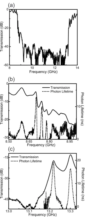
The 2D PC used in the experiments is a 25× 25 square array of cylindrical alumina rods whose radius is 1.55 mm and dielectric constant is 9.61. The separation between the center of rods along lattice vectors is a = 11 mm. The structure that we have used in our experiments has a filling fraction of 0.062. The photonic band structure and the corresponding eigenvectors are calculated by plane wave expansion method. Figure 1 shows the photonic band structure of the corresponding infinite photonic crystal for the first four TM polarized (Electric field is parallel to the axis of the rods) bands. According to the band structure calculations the lower band edge of the first band gap along Γ− X is at 8.70 GHz and, the upper band edge of the first band gap along Γ − X is at 13.20 GHz.
We have measured the transmission properties and the photon lifetime of the PC along Γ− X direction. The transmission measurement (Fig. 2(a)) indicates that the lower edge of the first band gap along Γ− X direction is around 8.7 GHz and the upper edge is around 13.2 GHz. These values are in agreement with the photonic band structure (Fig. 1). The measured photon lifetimes around the lower band edge and the upper band egde are shown in Fig. 2(b) and Fig. 2(c), respectively. As shown in both figures, the delay time significantly increases near the band edges. The photon lifetime near the lower edge is 12.9 nsec, which is 14× larger than the time required for the EM waves to propagate along the structure (0.92 nsec). So, the PC reduces the group velocity of light at this frequency by a factor of 14. For the upper edge, the lifetime is 19.2 nsec, which corresponds to a 22 times reduction for the speed of light.
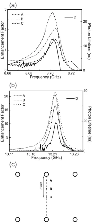
The enhancement factor for the EM waves emitted from a monopole source along Γ−X direction is measured for various source locations inside the center cell of the photonic crystal. The enhancement factor is defined as the ratio of the intensity of the EM waves emitted from a source located inside the photonic crystal to the intensity of the EM waves emitted from a source in free space. Figures 3(a) and 3(b) show the enhancement factors measured at various source locations inside the center unit cell for frequencies near the lower edge and the upper edge, respectively. The source locations are shown in Fig. 3(c). Although enhancement of radiation is expected for the band edge modes, the enhancement factor is not the same at all of the source locations. The enhancement factors presented in Fig. 3(a) and Fig. 3(b) show that the enhancement factor decreases for the lower band edge and increases for the upper band edge as we move the source away from the center rod. This
Figure 2. a) Transmission along Γ − X between 8 GHz and 14 GHz. b) Solid curve represents transmission and dashed
curve represents photon lifetime for the lower band edge along Γ− X direction. c) Solid curve represents transmission and dashed curve represents photon lifetime for the upper band edge along Γ− X direction.
can be explained by the fact that the emission of radiation depends on the intensity of the modes at the source location. The modes of the lower band edge are dielectric modes, while the modes of the upper band edge are air modes. Hence, as we move the source away from the center rod, LDOS and correspondingly, the enhancement factor is expected to decrease for the lower band edge and increase for the upper band edge. We also observe that the maximum enhancement factor for the upper band edge is higher than the enhancement factor for the lower band edge. This can be attributed to two major factors. First, for the lower band edge the electric field intensity of the mode is high inside the high dielectric material. Since the high dielectric region of the photonic crystal is not experimentally accessible, the possible highest enhancement factor can not be measured for the lower band edge. Second, the higher bands are flatter than the lower bands. This results in lower group velocities for the upper band edge for a finite photonic crystal.24 Hence, we expect LDOS and enhancement factor to be higher for the upper band edge when compared to the lower band edge.
2.2. Monopole Inside a Cavity
In the previous sections, we have emphasized the dependence of LDOS and enhancement factors on the intensity of the modes at the source locations and on the group velocities of the modes. In this sense, single cavity structures are promising structures for the control of emission from radiation sources, as the intensity of the cavity mode is localized and the group velocity for the cavity mode is reduced. Single cavity structures have been investigated by several authors.25–29 A variety of applications utilizing cavity structures have been proposed, such as single-mode light-emitting diodes,30 resonant antennas,31 optical filters32and resonant cavity enhanced detectors.33
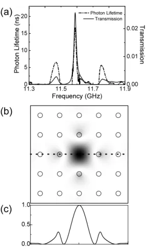
We have removed the center rod from a 9× 9 square array of alumina rods to create the single cavity structure. The measured transmission and the delay data for the single cavity structure are shown in Fig. 4(a). The transmission data indicates that the defect mode is around 11.6 GHz with a peak transmission of 0.025. The photon lifetime measurement shows an increase in the photon lifetime by a factor of 48. This also means that at the defect mode the group velocity is 48 times smaller when compared to the electromagnetic waves propagating in free space. In addition to the reduced group velocity, the computed mode profile in Fig. 4(b) shows that the intensity of the cavity mode is localized inside the cavity. Hence, at the cavity mode we expect to observe high enhancement factors for a monopole source located inside the cavity. Figure 5(a) shows the measured enhancement factor along Γ− X direction for various source locations inside the cavity. Enhancement factor measurements for the cavity structure show that as we move the source towards the center of the cavity, the cavity frequency shifts to higher frequencies. This is due to the modification of the cavity by the finite size of the radiation source. We also observe that as we move the source towards the center, the enhancement factor for the corresponding cavity mode increases. Maximum enhancement factor is obtained when the source is located at the center of the cavity. This can be explained by the LDOS picture. Since the intensity of the cavity mode increases towards the center of the cavity, LDOS is expected to increase as we move the radiation source towards the center of the cavity.
2.3. Angular Distribution of Power Emitted from a Monopole Source
The modes at the band edges of a PC are propagating modes and these modes are concentrated in low or high dielectric material region. Hence, the surface of the PC can be regarded as a system of radiation sources all operating at the band edge frequency, having similar spatial and temporal distribution of power with a uniform phase difference between the radiators.15 This system of radiators is similar to an array of antennas. Since all the radiators of the system radiate in Γ− S direction, we expect the emitted power from a source embedded inside the PC to be confined to a narrow angular region.
We carried out the measurements and the calculations for various frequencies. The measured far field radiation patterns for a square array of 32×20 alumina rods at various frequencies near the upper band edge are presented in Fig. 6. The minimum half power beam width is obtained at 13.21 GHz and it is found to be 8◦. Figure 6 shows that the angular distribution of power strongly depends on the radiation frequency. The radiation patterns are wider for frequencies higher than the upper band edge frequency. This can be explained by the presence of equal frequency modes along different directions at frequencies higher than the upper band edge frequency.
Figure 3. a) Enhancement factor near the lower band edge along Γ − X for a source located at A: 0.1 × a, B: 0.3 × a,C:
0.5 × a away from the center rod. D: represents the measured photon lifetime b) Enhancement factor near the upper band edge along Γ− X for a source located at A: 0.1 × a, B: 0.3 × a,C: 0.5 × a away from the center rod. D: represents the measured photon lifetime c) A, B, and C show the source locations that are used in Figures 3(a) and 3(b).
0.0 0.5 1.0 11.30 11.5 11.7 11.9 5 10 15 20 0.00 0.01 0.02 P hoto n L ife time (ns) Frequency (GHz) Photon Lifetime Transmission Tran smi ss ion
(a)
(b)
(c)
Figure 4. a) Solid curve represents transmission and dashed curve represents photon lifetime for the cavity mode. b)
Contour plot of electric field intensity for the cavity mode. Electric field intensity has been calculated by plane wave expansion method. A 5× 5 supercell has been used in the calculation. c) Intensity of the electric field for the cavity mode along the cross section shown with dotted line in Fig. 4(a)
Figure 5. a) Enhancement factor for a source located inside a cavity A: 0.2 × a, B: 0.4 × a, C: 0.6 × a, D: 0.8 × a, E:
1× a away from the rod. b) A, B, C, D, and E show the source locations that are used in Fig. 7(a)
0 30 60 90 120 150 180 -35 -25 -15 -5 13.15 GHz 13.25 GHz 13.30 GHz Band edge No rm al iz ed In te n si ty (d B )
Figure 6. Measured far field radiation patterns for various frequencies near the upper band edge. The crystal size is
10.0 10.2 10.4 -30 -20 -10 0 0 5 10 15 Tr an sm is si on ( dB ) Frequency (GHz) Phot on L ife time ( ns ) 10 12 14 16 -60 -40 -20 0 Experiment Tr an sm is si on (d B ) Frequency (GHz) FDTD Simulation
(a)
(b)
Figure 7. a) Transmission along the stacking direction between 10 GHz and 17 GHz b) Solid curve represents transmission
and dashed curve represents photon lifetime for the lower band edge along the stacking direction.
10.00 10.2 10.4 5 10 15
Enhancement
Factor
Frequency (GHz)
Figure 8. Enhancement factor around the lower band edge along the stacking direction.
2.4. Radiation from sources embedded inside three-dimensional photonic crystals
The PC that we used in our experiments is a 3D layer-by-layer structure,34, 35 which consists of square shaped alumina bars of alumina rods. The stacking sequence repeats every four layers, which has the equivalent geometry of a face centered tetragonal (fct) lattice, corresponding to a single unit cell in the stacking direction. The PC has 11 unit cells in the stacking direction. The dimensions of the alumina rods are 0.32 × 0.32 × 15.25 cm and dielectric constant of the rods is 9.61. The periodicity along the stacking direction is 1.28 cm. The parallel rods have a center to center separation of 1.12 cm, with a dielectric filling ratio of ∼ 0.29.
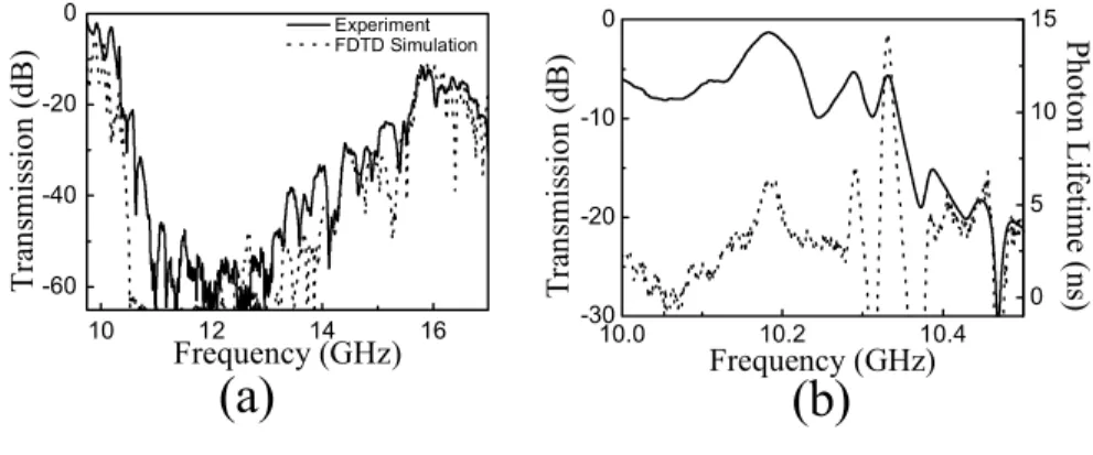
We have measured the transmission properties and the photon lifetime of the PC along the stacking direction. The transmission measurement (Fig. 7(a)) shows that the lower band edge (maximum of the first band) along stacking direction is around 10.3 GHz and the upper edge is around 15 GHz. The measured photon lifetimes around the lower band edge are presented in Fig. 7(b). The photon lifetime near the lower edge is 14.2 nsec. The time required for the EM waves to propagate along the structure which is 0.47 nsec. So, the PC reduces the group velocity of light at this frequency by a factor of 30.
The enhancement factor for the EM waves emitted from a monopole source along the stacking direction is measured. The monopole source is located at the center of the PC. Figure 8 shows the enhancement factor for frequencies near the lower edge. A maximum enhancement factor of 13.7 is obtained at 10.3 GHz, which also corresponds to the lower band edge frequency.
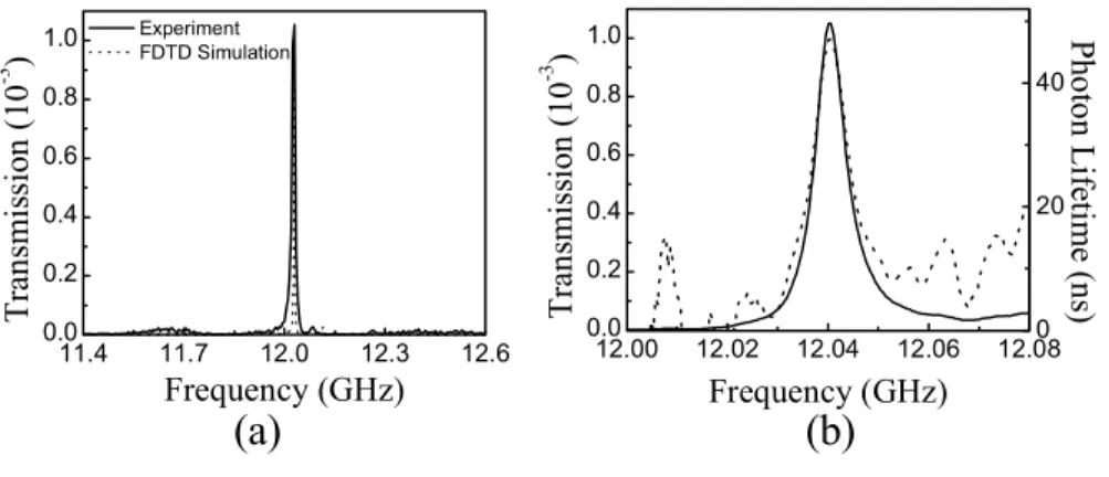
11.4 11.7 12.0 12.3 12.6 0.0 0.2 0.4 0.6 0.8 1.0 Experiment FDTD Simulation T ra nsm is sio n ( 10 -3 ) Frequency (GHz) 12.00 12.02 12.04 12.06 12.08 0.0 0.2 0.4 0.6 0.8 1.0 0 20 40 T ra nsm is si on ( 10 -3 ) Frequency (GHz) P hot on L ife tim e ( ns )
(a)
(b)
Figure 9. a) Calculated and measured transmission of the cavity mode b) Solid curve represents transmission and dashed
curve represents photon lifetime for the cavity mode.
11.9 12.0 12.1 12.2 0 5 10 15 20
Enhancement Factor
Frequency (GHz)
Figure 10. Enhancement factor for a monopole source located inside a cavity.
0 30 60 90 120 150 180 Experiment FDTD Simulation Intensity 0 5 10 15 0 30 60 90 120 150 180 Experiment FDTD Simulation Int en sity 0 5 10
(a)
(b)
Single cavity structures are very important features for the control of emission from radiation sources. Reso-nant cavity enhanced detectors36 and waveguide applications37were demonstrated using localized modes of the cavities built in photonic crystals. In order to obtain a single cavity localized in the photonic crystal, we have removed the center rod of a 20-layer 3D PC. The measured transmission and photon lifetime for the single cavity structure are shown in Fig. 9. The defect mode is at 12.04 GHz with a Q-factor (quality factor, defined as the center frequency divided by the full width at half maximum) of 1430. The photon lifetime at the defect mode frequency is 47 nsec. This also means that at the defect mode the group velocity is reduced by a factor of 220 when compared to the electromagnetic waves propagating in free space. The measured enhancement factor for the EM waves emitted from a monopole source embedded inside the cavity is shown in Fig 10. The enhancement factor is around 20 at 12.07 GHz. Compared to the enhancement factor that we obtained in 2D system, our 3D cavity exhibits 4 times larger enhancement factor. Our results show that 3D PCs can be used to enhance the emitted power from a monopole source.
The modes at the band edges of a PC are propagating modes and these modes are concentrated in low or high dielectric material region. Hence, the surface of the PC can be regarded as a system of radiation sources all operating at the band edge frequency, having similar spatial and temporal distribution of power with a uniform phase difference between the radiators.15 This system of radiators is similar to an array of antennas. Since all the radiators of the system radiate in Γ− S direction, we expect the emitted power from a source embedded inside the PC to be confined to a narrow angular region. Due to the 3D band gap, the angular confinement is also in 3 dimensions.
We have measured the angular distribution of power at the lower band edge frequency for E and H planes. For antennas with one narrow major lobe and very negligible minor lobes in the radiation pattern, the maximum directivity is given as38
D0∼= 4π
Θ1Θ2 (1)
where Θ1 is half power beam width of one plane (E-plane) and Θ2 is the perpendicular plane to the first (H-plane), in radians. The measured half power beam widths along the E- plane and H-plane are presented in Fig. 11. We have measured half power beam widths of 13o for both E and H planes. The directivity of the radiation source embedded inside 3D PC is calculated as 245.
3. CONCLUSION
In summary, we studied the emission of radiation from a monopole source located inside a photonic crystal and defect structure created in a photonic crystal. We showed the enhancement of radiation along with reduced group velocities at the band edges. Enhancement factor for a source depends on the group velocity of the mode and on the intensity of the electric field at the source location. We have also demonstrated that by using PCs it is possible to confine the emitted power to a narrow angular region for a source embedded inside a PC and radiating at the band edge frequency. Moreover, we have demonstrated that for a source embedded inside a 3D PC, it is possible to confine the emitted power to a narrow angular region in two planes for frequencies at the band edge frequency. We have measured half power beam widths of 13ofor both E and H planes, corresponding to maximum directivity of 245. The findings of our work can be used to improve the performance of certain devices such as antennas and LED’s.
4. ACKNOWLEDGMENTS
This work was supported by European Union under the projects EU-DALHM, EU NOE-METAMORPHOSE, EU NOE- PHOROMOST and by Turkish Department of Defense Grant No. KOBRA-002. One of the authors (Ekmel Ozbay) acknowledges partial support from Turkish Academy of Sciences.
REFERENCES
1. S. John, Phys. Rev. Lett. 58, 2486 (1987).
2. E. Yablonovitch, Phys. Rev. Lett. 58, 2059 (1987).
3. J. D. Joannopoulos, R. D. Meade, and J. N. Winn, Photonic Crystal: Molding the Flow of Light (Princeton University Press, Princeton, NJ, 1995.).
4. O. Painter, R. K. Lee, A. Scherer, A. Yariv, J. D. O’Brien, P. D. Dapkus, and I. Kim, Science 284, 1819 (1999).
5. B. Temelkuran, M. Bayindir, E. Ozbay, R. Biswas, M. M. Sigalas, G. Tuttle, and K. M. Ho, J. Appl. Phys.
87, 603 (2000).
6. K. Busch and S. John, Phys. Rev. Lett. 83, 967 (1999).
7. F. De Martini, M. Marrocco, P. Mataloni, and D. Murra, J. Opt. Soc. Am. B 10, 360 (1993).
8. P. R. Villenevue, S. Fan, J. D.Joannopoulos, K. Y. Lim, G. S. Petrich, L. A. Kolodjeski, and R. Reif, Appl. Phys. Lett. 67, 167 (1995).
9. P. L. Gourley, J. R.Wendt, G. A. Vawter, T. M. Brennan, and B. E. Hammons, Appl. Phys. Lett. 6, 687 (1994)
10. J. P. Dowling, M. Scalora, M. J. Bloemer, and C. M. Bowden, J. Appl. Phys. 75, 1896 (1994). 11. E. R. Brown, C. D. Parker, and E. Yablonovitch, J. Opt. Soc. Am. B 10, 404 (1993).
12. E. R. Brown and O. B. McMahon, Appl. Phys. Lett. 68, 1300 (1996).
13. R. Gonzalo, P. de Maagt, and M. Sorolla, IEE Trans. Microwave Theory Tech. 47, 2131 (1999) 14. I. Bulu, H. Caglayan, and E. Ozbay, Appl. Phys. Lett. 83, 3263 (2003).
15. I. Bulu, H. Caglayan, and E. Ozbay, Phys. Rev. B 67, 205103 (2003). 16. M. Bayindir and E. Ozbay, Phys. Rev. B 62, R2247-R2250 (2000).
17. S. Yano, Y. Segawa, J. S. Bae, K. Mizuno, S. Yamaguchi, and K. Ohtaka, Phys. Rev. B 66, 075119 (2002). 18. T. Kondo, M. Hangyo, S. Yamaguchi, S. Yano, Y. Segawa, and K. Ohtaka, Phys. Rev. B 66, 033111 (2002). 19. K. Ohtaka, Y. Suda, S. Nagano, T. Ueta, A. Imada, T. Koda, J. S. Bae, K. Mizuno, S. Yano, and Y. Segawa,
Phys. Rev. B 61, 5267 (2000).
20. K. Ohtaka, J. Lightwave Technology 17, 2161 (1999).
21. A. Imhof, W. L. Vos, R. Sprik, and A. Lagendijk, Phys. Rev. Lett. 83, 2942-2945 (1999).
22. K. Inoue, N. Kawai, Y. Sugimoto, N. Carlsson, N. Ikeda, and K. Asakawa, Phys. Rev. B 65, 121308 (2002). 23. T. Aoki, M. Wada Takeda, J. W. Haus, Z. Yuan, M. Tani, K. Sakai, N. Kawai, and K. Inoue, Phys. Rev. B
64, 045106 (2001).
24. D.-Y. Jeong, Y. H. Ye, and Q. M. Zhang, J. Appl. Phys. 92, 4194 (2002).
25. E. Ozbay, G. Tuttle, M. Sigalas, C. M. Soukoulis, and K. M. Ho, Phys. Rev. B 51, 13961(1995). 26. M. M. Sigalas, K. M. Ho, R. Biswas, and C. M. Soukoulis, Phys. Rev. B 57, 3815 (1998).
27. C. J. M. Smith, R. M. De La Rue, M. Rattier, S. Olivier, H. Benisty, C. Weisbuch, T. F. Krauss, R. Houdr´e, and U. Oesterle, Appl. Phys. Lett. 78, 1487 (2001).
28. T. Ochiai and J. S´anchez-Dehesa, Phys. Rev. B 65, 245111 (2002).
29. S. Lan, S. Nishikawa, Y. Sugimoto, N. Ikeda, K. Asakawa, and H. Ishikawa, Phys. Rev. B 65, 165208 (2002). 30. I. Schnitzer, E. Yablonovitch, A. Scherer, and T. J. Gmitter, Photonic Band Gap and Localization, C. M.
Soukoulis, Ed., 1993, vol. 308, NATO ASI SERIES B., pp.369-378.
31. B. Temelkuran, M. Bayindir, E. Ozbay, R. Biswas, M. M. Sigalas, G. Tuttle, and K. M. Ho, J. Appl. Phys.
87, 603 (2000).
32. J. D. Joannopoulos, Photonic Band Gap Materials, C. M. Soukoulis, Ed., 1996, vol. 315, NATO ASI SERIES E., pp.1-21.
33. B. Temelkuran, E. Ozbay, J. P. Kavanaugh, G. Tuttle, and K. M. Ho, Appl. Phys. Lett. 72, 2376 (1998). 34. E. Ozbay, J. Opt. Soc. Am. B 13, 1945 (1996)
35. K. M. Ho, C. T. Chan, C. M. Soukoulis, R. Biswas, and M. Sigalas, Solid State Commun. 89, 413 (1994). 36. B. Temelkuran, E. Ozbay, J. P. Kavanaugh, G. Tuttle, and K. M. Ho, Appl. Phys. Lett. 72, 2376 (1998). 37. M. M. Sigalas, R. Biswas, K. M. Ho, C. M. Soukoulis, D. Turner, B. Vasiliu, S. C. Kothari, and S. Lin,