SILICON GERMANIUM MULTI QUANTUM
WELLS FOR HIGH EFFICIENCY
OPTOELECTRONIC DEVICES
A THESIS
SUBMITTED TO THE DEPARTMENT OF ELECTRICAL AND ELECTRONICS ENGINEERING
AND THE INSTITUTE OF ENGINEERING AND SCIENCES OF IHSAN DOGRAMACI BILKENT UNIVERSITY IN PARTIAL FULLFILMENT OF THE REQUIREMENTS
FOR THE DEGREE OF MASTER OF SCIENCE
By
Alper Yeşilyurt
March 2011
ii
I certify that I have read this thesis and that in my opinion it is fully adequate, in scope and in quality, as a thesis for the degree of Master of Science.
Assist. Prof. Dr. Ali Kemal Okyay (Supervisor)
I certify that I have read this thesis and that in my opinion it is fully adequate, in scope and in quality, as a thesis for the degree of Master of Science.
Assoc. Prof. Dr. Hilmi Volkan Demir
I certify that I have read this thesis and that in my opinion it is fully adequate, in scope and in quality, as a thesis for the degree of Master of Science.
Assist. Prof. Dr. Coşkun Kocabaş
Approved for the Institute of Engineering and Sciences:
Prof. Dr. Levent Onural
iii
ABSTRACT
SILICON GERMANIUM MULTI QUANTUM WELLS
FOR HIGH EFFICIENCY OPTOELECTRONIC DEVICES
Alper Yeşilyurt
M.S. in Electrical and Electronics Engineering
Supervisor: Assist. Prof. Dr. Ali Kemal Okyay
March 2011
Silicon (Si) based complementary metal-oxide-semiconductor (CMOS) technology provides a low cost platform and reproducible processing for electronic signal processing and electronic industry has significantly flourished in terms of increased device densities and speeds. All the same, advanced CMOS processes associated with the very large scale integrated (VLSI) circuits are required for the fabrication of today’s advanced microprocessors comprising billions of transistors per single chip with higher operational data rates. Herein, increasing trend for the speed of current circuits is hampered due to the delays of electrical interconnects that basically arise from RC factor. Signal attenuation due to power dissipation and electromagnetic interference issues are further physical bottlenecks that affect the performance of current technology. At this point, an idea proposes the development of optical interconnect network layers on Si CMOS circuitry operating at telecommunications wavelength range (~1.3-1.5 µm). This promising conception enables optical information processing and offers a platform that overcomes the physical restrictions of electrical interconnects. Si based optoelectronic devices are near-infrared-blind due to large indirect (~1.12 eV) and direct band gap (~3.4 eV) energies. To date, III-V compounds and especially InGaAs based detectors are “state-of-the-art” optical devices that are used for near-infrared (NIR) applications. However, due to high material cost and difficult integration with Si CMOS technology they
iv
have limited market growth. At this point, germanium (Ge) is a promising candidate for NIR applications with its suitable indirect (~0.66 eV) and direct (~0.8 eV) band gap, which overcomes spectral limitations of Si. Additionally, lattice mismatch (~4.2%) problem among Si and Ge is worked out by novel heteroepitaxial growth technique (MHAH), which reduces the threading dislocations and enables the monolithic integration with conventional CMOS technology. For the scope of the thesis, fabrication, material characterization and device characterizations of p-i-n photodetector and electro-absorption modulator architectures, which are the key elements of a basic optical interconnect structure, are performed. Ge/SixGe1-x multi quantum well (MQW) structures are
utilized in the intrinsic layer to exploit the electro-absorption mechanism of quantum-confined Stark effect (QCSE). Represented photodetectors exhibit low dark current (~5 mA/cm2 at -1 V) and high responsivity (~0.33 A/W at 1310 nm and 0 V). Demonstrated electro-absorption modulators exhibit very high absorption coefficient contrast (3.41 at 1550 nm and 3 V) especially for conventional C-band (1530-1565 nm) telecommunication wavelength range and low insertion loss (0.2 dB at 1540 nm). Modulation performance is highly comparable with the electro-absorption modulators based on direct gap III-V compounds at the wavelength range of interest. Demonstrated photodetector and electro-absorption modulators are the high performance building blocks of an optical interconnect system.
Keywords: SiGe, photodetector, electro-absorption modulator, quantum well,
v
ÖZET
SİLİSYUM GERMANYUM ÇOKLU KUANTUM
KUYULARI İÇEREN YÜKSEK VERİMLİ
OPTOELEKTRONİK AYGITLAR
Alper Yeşilyurt
Elektrik ve Elektronik Mühendisliği Bölümü Yüksek Lisans Tez Yöneticisi: Yar. Doç. Dr. Ali Kemal Okyay
Mart 2011
Silisyum (Si) tabanlı tümler metal-oksit-yarıiletken (CMOS) teknolojisi elektronik sinyal işleme için düşük maliyetli ve tekrarlanabilir bir üretim ortamı sağlar. Elektronik endüstrisi aygıt hızları ve yoğunlukları göz önüne alındığında önemli ölçüde gelişti. Bununla birlikte, bugünün tek bir tümdevrede yüksek işlemsel veri hızına sahip milyonlarca tranzistörler içeren mikroişlemcilerin fabrikasyonu için çok büyük çapta tümleşik (VLSI) elektronik devreler içeren gelişmiş CMOS işlem süreçleri gerekmektedir. Bu noktada, bugünün devrelerinin artan hız eğilimi elektriksel arabağlantıların RC çarpanından kaynaklanan gecikmeler nedeniyle büyük ölçüde duraksama yaşadı. Güç yitimi ve elektromanyetik girişim sorunlarından kaynaklanan sinyal zayıflaması bugünün teknolojisinin başarımını etkileyen fiziksel engellerdir. Bu noktada, Si CMOS devrelerinin üzerine iletişim dalga boylarında çalışan (~1.3-1.5 µm) optik arabağlantı ağları kurulması fikri ön plana çıkar. Bu gelecek vaat eden fikir elektriksel bağlantıların fiziksel engellerini ortadan kaldıran optik bilgi işleme ortamı sunar. Si tabanlı optoelektronik aygıtlar indirekt (~1.12 eV) ve direkt (~3.4 eV) yasak bant enerjileri nedeniyle yakın kızılberisi dalgaboylarında kördür. Bugüne kadar, III-V grubu bileşikler ve özellikle InGaAs tabanlı algılayıcılar yakın kızılberisi uygulamalar için en gelişmiş aygıtlardır. Fakat,
vi
malzeme maliyetlerinin yüksekliği ve Si CMOS teknolojisiyle tümleşim zorlukları nedeniyle sınırlı piyasa büyümesine sahiptir. Bu noktada, Germanyum (Ge), indirekt (~0.66 eV) ve direkt (~0.8 eV) yasak bant enerjileri sayesinde Silisyumun spektral sınırlamalarının üstesinden gelerek yakın kızılberisi dalgaboylarındaki uygulamalar için umut vaat eder. Ayrıca, dislokasyonları azaltan ve geleneksel CMOS teknolojisiyle tektaş tümleşimi sağlayan yeni geliştirilmiş bir heteroepitaksi yöntemi (MHAH) sayesinde Si ve Ge arasındaki örgüsel uyumsuzluk sorunu çözülmüştür. Bu tez kapsamında, optik arabağlantı yapılarının temel öğeleri olan p-i-n fotoalgılayıcı ve elektrosoğrulma kipleyicisi mimarilerinin fabrikasyon, aygıt ve malzeme karakterizasyonu gerçekleştirildi. Bir elektrosoğrulma mekanizması olan kuantum sınırlamalı Stark etkisini (QCSE) kullanmak amacıyla Ge/SixGe1-x çoklu kuantum kuyusu (MQW)
yapıları p-i-n mimarilerinin katkısız kısımlarında kullanılmıştır. Gösterilen fotoalgılayıcılar düşük karanlık akımı (~5 mA/cm2 ve -1 V) ve yüksek duyarlılık (~0.33 A/W, 1310 nm ve 0 V) sergiledi. Gösterilen elektrosoğrulma kipleyicileri özellikle C-bantı (1530-1565 nm) iletişim dalgaboyu alanında olmak üzere çok yüksek soğrulma katsayısı kontrastı (3.41, 1550 nm ve 3 V) sergiledi. Alakalı dalga boylarındaki III-V tabanlı elektrosoğrulma kipleyiciler ile çok benzer kiplenim başarıları sağlandı. Gösterilen fotoalgılayıcılar ve elektrosoğrulma kipleyicileri optik arabağlantı sistemlerinin yüksek başarımlı yapıtaşlarıdır.
Anahtar Kelimeler: SiGe, fotoalgılayıcı, elektrosoğrulma kipleyicisi, kuantum
vii
Acknowledgements
I would like to express my profound gratitude to my supervisor, Dr. Ali Kemal Okyay for his friendly and understanding supervision and guidance throughout this work. He was always ready in the case of any hesitation and offer fruitful suggestions. I have learned a lot from him.
I would also like to thank all Okyay research team members who have contributed to my research experience and all my mates & colleagues including Engin, Temmuz, Ahmet, Gürkan, Mustafa, Çağla, Akın, İnci, Özgür, Fatih, …
Sincere thanks go to Dr. Hilmi Volkan Demir and Dr. Coşkun Kocabaş for being in my thesis committee and sharing their worthy comments. I am also indebted to Dr. Hilmi Volkan Demir for authorizing me to share Demir research group labs and Dr. Bülend Ortaç for his useful comments and help regarding optical characterization set-up.
Above all, I would like to thank my family and especially my grandmother for their endless support. I would like to thank Damla for her love and continuous encouragement. This work would not have been possible without them and this thesis is dedicated to them.
viii
Table of Contents
Abstract ... iii Özet ... v Acknowledgements ... vii Contents ... viii List of Figures ... xList of Tables ... xiii
1 INTRODUCTION ... 1
1.1 Problem Statement ... 1
1.2 Motivation ... 4
1.3 Objectives ... 7
1.4 Organization of the Thesis ... 7
2 OPTOELECTRONIC DEVICE PHYSICS ... 8
2.1 Photodetector Overview ... 8
2.1.1 p-i-n Photodetector ... 9
2.1.2 p-i-n Photodetector Characteristics ...10
2.1.2.1 Current-Voltage (I-V) ... 10
2.1.2.2 Quantum Efficiency ... 12
2.1.2.3 Responsivity ... 13
2.2 Optical Modulator Overview ... 13
2.2.1 Quantum Confinement ... 14
2.2.2 Electro-absorption Effect ... 16
2.2.2.1 Franz-Keldysh Effect (FKE) ... 16
2.2.2.2 Quantum-Confined Stark Effect (QCSE) ... 17
2.2.3 Electro-absorption Modulator Characteristics ... 19
2.3 SiGe Research Review ... 21
2.3.1 p-i-n Photodetector Literature Review ... 21
2.3.2 p-i-n Electro-absorption Modulator Literature Review ... 24
3 DEVICE FABRICATION ... 26
3.1 Substrate and Surface Preparation ... 26
3.2 Patterning ... 27
3.3 Dry Etching ... 28
3.4 Dielectric Film Coating ... 29
3.5 Wet Etching ... 30
ix
4 OPTOELECTRONIC DEVICE CHARACTERIZATION ... 32
4.1 Material Characterization ... 32
4.1.1 Nanostructural Characterization ... 32
4.1.2 Multi Quantum Well (MQW) Band Structure ... 36
4.2 Device Optoelectronic Characterization ... 39
4.2.1 Current-Voltage (I-V) ... 39
4.2.1.1 Dark Current ... 39
4.2.1.2 Illuminated Current (AM1.5G) ... 42
4.2.2 Responsivity and Quantum Efficiency ... 43
4.2.2.1 Photodetector Characterization ... 46
4.2.2.2 Optical Modulator Characterization ... 47
5 CONCLUSIONS AND FUTURE DIRECTIONS ... 53
APPENDIX ... 54
A - SIGE HETEROSTRUCTURE GROWTH: MULTIPLE HYDROGEN ANNEALING FOR HETEROEPITAXY (MHAH) BIBLIOGRAPHY ... 57
x
List of Figures
Figure 1.1 - Differences between optics and electronics expressed in terms of wavelength, frequency and photon energy ... 2
Figure 1.2 - Optical and electrical propagation in terms of loss and velocity .. 2 Figure 1.3 - On-chip optical interconnection system ... 3
Figure 1.4 - Electrical and optical interconnection system ... 3
Figure 1.5 - Absorption coefficient vs. Photon energy (and wavelength) for various semiconductors ... 5
Figure 2.1 - Electron-hole photogeneration in a semiconductor ... 9
Figure 2.2 - a) Top illuminated p-i-n photodetector structure, b) Corresponding band diagram, charge and electric field distribution ... 10
Figure 2.3 - p-i-n photodetector operation under illumination ... 12
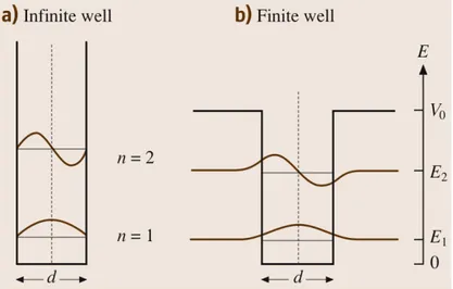
Figure 2.4 - a) Quantum well with infinite barriers and confined energy states, b) Quantum well with finite barriers (V0) and confined energy states ... 16
Figure 2.5 - Schematic illustration of Franz-Keldysh effect ... 17 Figure 2.6 - Schematic illustration of QCSE ... 18
Figure 2.7 - Electro-absorption spectra of p-i-n Ge/SiGe MQW structure exploiting QCSE ... 19
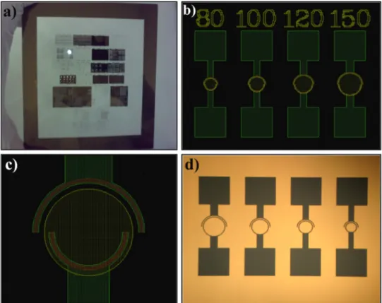
Figure 2.8 - Electro-absorption modulator operation schematic representation 20 Figure 3.1 - a) Photolithography mask, b) Multi-level CAD design of p-i-n structures, c) Multi-level design (closer view), d) Optical micrograph image of metallization lift-off mask ... 27
Figure 3.2 - a) Top view of the circular mesa structures on ZYGO optical profilometer program, b) Schematic 3D representation of one of the etched samples, c) Scan results of ZYGO optical profilometer ... 29
Figure 3.3 - a) Optical micrograph image (top view), b) Schematic representation of the etched sample ... 30
xi
Figure 3.4 a) SEM micrograph image of final p-i-n device and schematic representation (inset), b) Optical micrograph image of devices with different MESA diameters, c) Optical micrograph image of one of the devices ... 31 Figure 4.1 - TEM images of p-i-n MQW structures (samples I18 and I19, respectively) ... 33
Figure 4.2 - XPS Study - Concentration profile in terms of depth (sample I19)
...34
Figure 4.3 - Photoluminescence spectra with excitation wavelength of 225 nm (sample I18) ...35
Figure 4.4 - Raman spectroscopy (sample I18, I19 and ref. Si wafer) ... 36 Figure 4.5 - Ge/SixGe1-x MQW band structure ... 37
Figure 4.6 - Band structures of a) Si, b) Ge, c) compressive strained Ge and d) tensile strained Ge-rich SixGe1-x ... 37
Figure 4.7 - Current-Voltage (I-V) characteristics (sample I18) ... 40 Figure 4.8 - Dark current vs. Mesa area at different bias voltages (sample I18 and I19, respectively) ... 41
Figure 4.9 - Dark & Illuminated (AM1.5G) I-V characteristics (sample I18) 42 Figure 4.10 - a) Schematic representation of optical characterization set-up and photograph of the b) general view of the set-up, c) light modulation part and d) fiber-to-detector coupling part ... 44,45
Figure 4.11 - Effective absorption coefficient for various bias voltages (sample
I18 with mesa diameter of 100 µm) ... 47
Figure 4.12 - Photocurrent (nA) vs. Wavelength (nm) for various bias voltages (sample I19 with mesa diameter of 120 µm) ... 48
Figure 4.13 - Responsivity (A/W) vs. Wavelength (nm) for various bias voltages (sample I19 with mesa diameter of 120 µm) ... 49
Figure 4.14 - Effective absorption coefficient spectra for various bias voltages (sample I19 with mesa diameter of 120 µm) ... 50
Figure 4.15 - Absorption coefficient contrast with respect to wavelength (sample
xii
Figure 4.16 - Contrast ratio & Insertion loss respect to wavelength (sample I19 with mesa diameter of 120 µm) ... 52
Figure A1 - ASM basic wafer-handling section drawing, courtesy of ASM Epitaxy ... 55
xiii
List of Tables
Table 1.1 - Band gap energy of Si, Ge, InAs and GaAs at 0 K and 300 K ... 6 Table 1.2 - Carrier mobilities of Si, Ge, InAs and GaAs at room temperature .. 6 Table 2.1 - Reported best dark current performances associated with the growth techniques ... 22
Table 2.2 - Reported best responsivity performances for different device structures ... 23
Table 2.3 - Reported electro-absorption modulator performances based on FKE and QCSE ... 24
Table 4.1 - Layer thicknesses of p-i-n MQW structures (samples I18 and I19).33 Table 4.2 - Band parameters and electron, heavy-hole energy levels (samples
I18 and I19) ... 39
Table 4.3 - Isc, Voc and Pmax and Fill factor for various mesa diameters (sample
I18) ... 42
Table 4.4 - Optical characterization data at 1310 nm and 0 V (sample I18 and
1
Chapter 1
Introduction
This thesis describes our recent developments on and contributions to complementary metal-oxide-semiconductor (CMOS) compatible optoelectronic device technology in terms of fabrication, characterization and analysis of novel devices. This chapter gives an overview of the problem and our motivation for carrying forward this work.
1.1 Problem Statement
Advances in the very large scale integration (VLSI) with the established Si CMOS technology have dramatically increased the device densities and speeds [1]. The traditional electrical interconnects based on Copper (Cu) metal wires and Aluminum (Al) interconnect lines mainly suffer from i) bandwidth limitation, ii) signal attenuation due to power dissipation, iii) electromagnetic interference issues [1-5]. These physical bottlenecks are the limiting factors for the performance of the current VLSI technology. According to the approach in 1984, Goodman et al. [2] have drawn attention by claiming that the speeds of CMOS circuits will be limited by interconnection delays of the devices. Meindl [3], similarly and exhaustively reviews the interconnect issue and mentions that the latency of the post-Moore’s Law interconnects will exceed that of the transistors for interconnect lengths greater than 30 µm, which reveals an interconnect era beyond Moore’s Law.
Integration of electrical and optical circuitry exhibits a promising solution for the interconnect issue. Development of optical interconnect network layers on Si CMOS circuitry offers a platform that fulfills the specific design requirements in terms of speed, power and bandwidth for chip-to-chip and also on-chip communication.
2
Figure 1.1 Differences between optics and electronics expressed in terms of wavelength, frequency and photon energy (After Ref. [4])
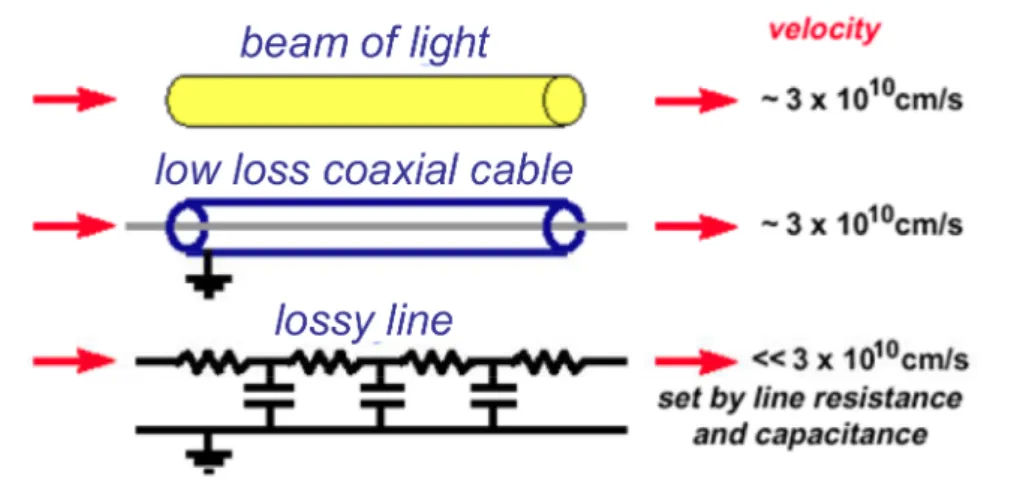
Figure 1.1 represents the substantial differences between optics and electronics in terms of wavelength, frequency and photon energy. Short wavelength of light enables confinement of light into low-loss dielectric waveguides (e.g. optical fiber), which provides low-loss propagation and directional manipulation of light. Electrical interconnect materials are lossy especially for high frequency signals due to skin effect. However, the carrier frequency of light is significantly high compared to electrical signals and any other practicable modulation frequency, which avoids frequency dependent loss. For the case of electrical interconnects, frequency dependent signal loss and distortion are substantial, either the line is LC with loss dominated by the skin effect, or it is RC with bulk resistive loss [6]. Figure 1.2 represents the propagation of optical and electrical signals in terms of loss and velocity.
3 Above all, large photon energy of light enables perfect voltage isolation between different parts of circuits. Figure 1.3 shows an on-chip optical interconnect system that composed of a light source with an optical modulator (transmitter part) and photodetector (receiver part) with corresponding integrated electrical circuitry [7].
Figure 1.3 On-chip optical interconnection system (After Ref. [7])
Additionally, voltage isolation exists between two parts, because photons do not carry electrical information about the transmitter part by themselves. Indeed, photodetector generates electrical signal from the modulated and waveguide-coupled light at the receiver side and feeds into electrical circuitry that converts into digital output signal.
Figure 1.4 Electrical and optical interconnection system (After Ref. [4])
Large photon energy also enables quantum impedance conversion. Impedance transformers are needed for a classical electrical interconnect which
4 is composed of a low-impedance electrical connection line with high-impedance devices. Optical devices match the optical signal to the electrical circuitry with the aid of the quantum detection and generation. Figure 1.4 shows the impedance matching for a classical electrical and optical interconnection system. Miller presents further essential and comprehensive research review and historical summary of the development of optical interconnects and physical reasons for the integration of optics with the Si CMOS circuitry based on solving the mentioned issues [4-5].
1.2 Motivation
Development of optoelectronic devices and growth technologies based on enabling the integration of optical and electrical circuitry becomes crucial due to the communication bottlenecks that arise from the defined physical restrictions of electrical interconnects. Established Si CMOS technology provides a low cost platform and reproducible processing for on-chip optical and electronic signal processing. A wide number of materials and processes are also available for optical device and interconnect fabrication, however, monolithic integration with Si CMOS microelectronics is the basic concern [7]. Optoelectronic device technology, based on group III-V compounds and especially InGaAs, offers increased functionality and high performance. As a result, the detectors based on these materials are the “state-of-the-art” optoelectronic devices for near-infrared (NIR) and especially fiber telecommunication bands (1.31-1.55 µm) detection applications [9-11]. This is due to, i) high tunability of direct band gap energy [12], ii) low dark current achievement using lattice matched materials [13]. Despite its advantages, high raw material costs and integration difficulty with the current Si CMOS technology [14-17] hampers the widespread growth of III-V interconnection technology. Furthermore, construction of optical interconnection architectures requires materials with monolithic integration ability with standard Si CMOS technology and absorption capability that overcomes silicon’s spectral limitation.
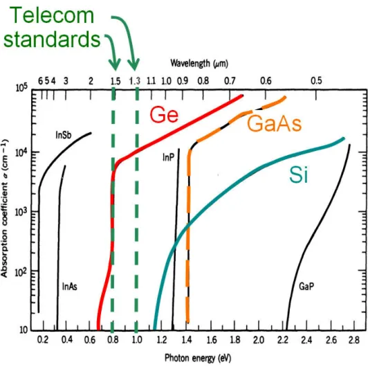
5 Germanium (Ge) shows great promise with high absorption coefficient for NIR telecommunication wavelength range (1.31-1.55 µm) thanks to its suitable energy band gap (Eg(direct) = 0.8 eV, Eg(indirect) = 0.66 eV). Silicon is blind and
silica fibers have low absorption and scattering losses [18] for the wavelength range of interest. Good transport properties also make Ge an attractive candidate for NIR photodetection and modulation. Figure 1.5 shows the spectral efficiency of Ge which spans wider absorption range over Si (Eg(indirect) = 1.1 eV) including
telecommunication standards wavelength spectra [19]. The potential of the monolithic integration of Ge with Si makes it an ideal candidate.
Figure 1.5 Absorption coefficient vs. Photon energy (and wavelength) for various semiconductors (After Ref. [19])
Table 1.1 and 1.2 shows the band gap energy and carrier mobilities of Si, Ge and III-V based compounds, respectively [20].
6
Table 1.1 Band gap energy of Si, Ge, InAs and GaAs at 0 K and 300 K (i=indirect gap, d=direct gap) (After Ref. [20])
Table 1.2 Carrier mobilities of Si, Ge, InAs and GaAs at room temperature, in cm2/V-s (After Ref. [20])
High quality and defect-free heteroepitaxial growth of Ge on Si is a challenging process due to large lattice mismatch (4.2%) and results with islanding and misfit dislocations that are formed at the Si substrate and Ge film interface terminating at the film surface as threading dislocations [21]. To date, different research groups demonstrated high performance optoelectronic devices by using epitaxial techniques based on employing a low temperature buffer layer associated with cyclic thermal annealing [22-24] and epitaxial growth of compositionally graded Si1-xGex buffer layers [25-27] to reduce the threading
dislocations.
Nayfeh et al. [21] concentrated on this issue by demonstrating a novel technique, multiple hydrogen annealing heteroepitaxy (MHAH), which enables the growth of high quality, low dislocation density and low surface roughness Ge films on Si [21], [28]. For this thesis work, material growth of high quality SixGe1-x layers associated with the quantum-confined structures is performed
7
1.3 Objectives
Previous research covers the demonstration of the growth of Ge on Si for high responsivity photodetectors [29-33] and high performance electro-absorption modulators [34-37] operating at telecommunication wavelengths. For development of alternative and promising approaches, objectives for this thesis are fabrication, material and device characterizations of SiGe based, integrated optoelectronic devices based on top-illuminated p-i-n architectures with grown SixGe1-x multi quantum well (MQW) structures for demonstrating i) high
responsivity and low dark current photodetectors, ii) high performance electro-absorption modulators exploiting quantum-confined Stark effect (QCSE).
1.4 Organization of the Thesis
This part of the chapter gives information about the progression of the thesis. Chapter 2 gives a review of operation principles of photodetectors and electro-absorption modulators offering a literature survey. Chapter 3 presents optoelectronic device fabrication of p-i-n layers composed of SixGe1-x MQW
structures. Chapter 4 discusses the material and device characterizations and analysis of p-i-n photodetector and electro-absorption modulator. Chapter 5 concludes the thesis with the conclusions and future suggestions.
8
Chapter 2
Optoelectronic Device Physics
This chapter provides a short overview on photodetection (specifically on p-i-n photodetectors) and optical modulation. Basic electro-absorption modulator operation is discussed with a sense of quantum-confinement concept based on quantum wells (QWs) and modulation mechanism of quantum-confined Stark effect (QCSE). This chapter further describes important performance parameters of photodetector and modulators. This chapter also offers a detailed review of recent literature on SiGe near-infrared photodetection and modulation.
2.1 Photodetector Overview
Semiconductor photodetector (photodiode) is essentially a p-n junction diode that converts incident optical radiation into electrical current. An incident photon with energy greater than the energy band gap of the semiconductor excites an electron to an upper energy level (conduction band) and leaves a hole (lack of electron) behind (valence band). The wavelength of the photon that carries an energy equal to the band gap energy is given as
€ λ= hc Eg ≈1.24 Eg (2.1) where € λ: wavelength (µm), €
h: Planck constant (eV·s),
€
c: velocity of light (m·s-1) and
€
Eg: band gap energy (eV)
Figure 2.1 illustrates the absorption of a photon resulting in electron-hole generation in a semiconductor [38]. Applied (or built-in) electric field enables the collection of this optically generated electron-hole pair (ehp) by drift process through the material. Moving ehp’s constitute photocurrent. Photons with energies higher than the band gap of the semiconductor contribute to the induced
9 photocurrent. This optical absorption process could be direct or indirect. Absorption of a photon requires a simultaneous momentum change (usually by a phonon) in indirect semiconductors (e.g. Si and Ge). Phonons are not involved for direct gap optical transitions.
Figure 2.1 Electron-hole photogeneration in a semiconductor (After Ref. [38])
Various photodetector structures (p-i-n, MSM, APD) exist with characteristic advantages, however this overview mainly concentrates on p-i-n photodetectors.
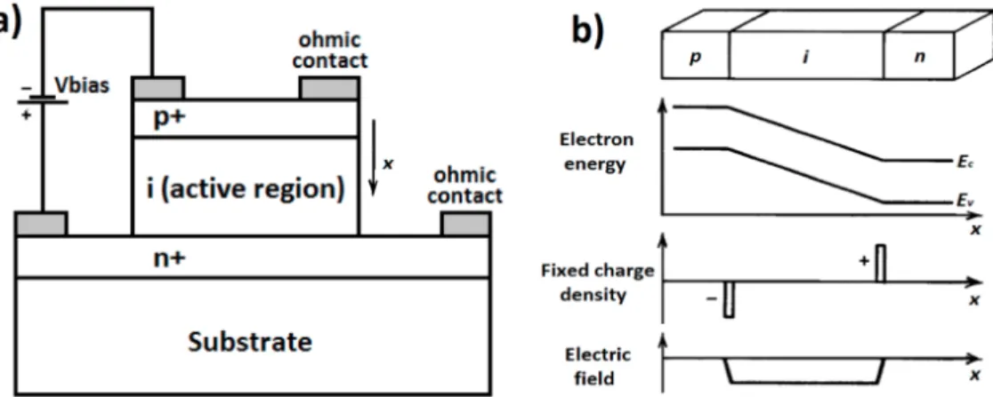
2.1.1 p-i-n Photodetector
A p-i-n photodetector consists of an intrinsic (undoped) region sandwiched between highly doped p-type and n-type regions with corresponding ohmic
contacts. Figure 2.2 a) illustrates a typical p-i-n photodetector structure. A conventional p-n junction diode, with highly doped p-type and n-type regions,
results with a quite thin depletion region, which implies relatively high junction capacitance. Moreover, carriers generated in the p-type and n-type regions can contribute to the photocurrent only by diffusing into the depletion region, otherwise they recombine in the doped regions [39]. The presence of a thick intrinsic region (typical p-i-n photodetector) allows the absorption of more photons resulting in a higher photocurrent. Wider depletion region, effectively spanning the intrinsic region, results in low device capacitance. This enables high-speed photodetection and increased bandwidth because of decreased
RC-related delays (assuming RC-limited, not transit time limited). Constant
10 carriers by drift process. The main challenge for a p-i-n photodetector is the demand for high quality material growth techniques and application of multi-step fabrication processes. Figure 2.2 b) depicts the corresponding band diagram, charge and electric field distribution across a conventional p-i-n device [12].
Figure 2.2 a) Top illuminated p-i-n photodetector structure, b) Corresponding band diagram, charge and electric field distribution (After Ref. [12])
2.1.2 p-i-n Photodetector Characteristics
Certain general metrics are used to evaluate the performance of photodetectors. Internal and external quantum efficiency, responsivity and bandwidth are extensively utilized for typical applications.
2.1.2.1 Current-Voltage (I-V) Characteristics
Typically p-i-n photodetectors are operated at reverse bias condition. Reverse leakage current associated with thermal generation and recombination of carriers in the depletion region corresponds to the dark current. Under reverse bias condition, diffusion current is negligible due to a high potential barrier and the thermally generated carriers determine the current (drift current). Under forward bias condition, diffusion of carriers determines the current and increase exponentially with the applied voltage. Total current in a p-i-n photodetector
11 (under no illumination) is the sum of diffusion and generation current and denoted by [41]: € I = qA Dp Lp pn + Dn Ln np ⎛ ⎝ ⎜ ⎜ ⎞ ⎠ ⎟ ⎟ (eqV / kT −1) = I0(e qV / kT −1) (2.2) where € Dn, €
Dp: diffusion coefficient for electrons and holes (cm2·s-1)
€
Ln,
€
Lp: electron and hole diffusion length (cm)
€
pn,
€
np: equilibrium concentration of holes in n-type material and electrons in p-type material (cm-3)
€
I0: reverse saturation current (A)
€
A: active device area (cm2)
In response to illumination with photons
€
hv > Eg, where
€
hv corresponds
to the photon energy with the specified frequency (
€
v = c /λ), carriers are
generated optically at a rate of gop.Photogenerated ehp’s in the depletion region
and within a diffusion length of the transition region make-up the photocurrent (Ip).
€
Ip = qAgop(Lp+ Ln + W ) (2.3)
where
€
W: depletion layer thickness (cm)
Total current (IT) across the device under illumination is the combination of eqns. (2.2) and (2.3): € IT = qA Dp Lp pn + Dn Ln np ⎛ ⎝ ⎜ ⎜ ⎞ ⎠ ⎟ ⎟ (eqV / kT −1) − qAgop(Lp + Ln + W )(2.4)
The photogenerated carriers are collected by drift process; and the minus sign in eqn. (2.4) is originating from the flow of photocurrent from n-type towards p-type region. Figure 2.3 is a schematic illustration of p-i-n photodetector operation under illumination [42].
12
Figure 2.3 p-i-n photodetector operation under illumination (After Ref. [42])
2.1.2.2 Quantum Efficiency (
€
η)
Internal quantum efficiency is a measure of the collection efficiency of photogenerated carriers. Typically internal quantum efficiency is above 90%, 10% loss attributed to recombination of small number of ehp’s before being completely collected. External quantum efficiency, on the other hand, is a performance metric that relates the number of collected ehp’s at the terminals to the incoming number of photons. External quantum efficiency (quantum efficiency) includes surface reflections, non-complete absorption of the incoming light (e.g. thin absorbing layers) in addition to internal quantum efficiency. Quantum efficiency (
€ 0 ≤η≤ 1) is defined as: € η λ
( )
= (1 − R) 1 − exp(−α λ[
( )
d)]
(2.5) where € η λ( )
: quantum efficiency, €R: optical reflectivity of the surface,
€
α λ
( )
: absorption coefficient of the material (cm-1),€
13 The quantum efficiency is wavelength dependent since the absorption coefficient (
€
α ) of a semiconductor has also wavelength dependency. For
€
λ >
€
λc, where
€
λc is the longest (cut-off) wavelength of absorption,
€
η is very small (nearly zero) making the material transparent at those wavelengths (eqn. (2.1)). For very small
€
λ (i.e. highly energetic photons),
€
η is small since most of the photons are absorbed in a region very close to the material surface. Photogenerated carriers are usually recombined at G-R centers due to crystal imperfections at the surface before they can be extracted. An ideal p-i-n photodetector is expected to absorb all incident photons inside the depletion region and generate one electron per an incident photon that contributes to the photocurrent [39].
2.1.2.3 Responsivity (
€
ℜ)
Responsivity is a measure of the optical to electrical conversion efficiency of a photodetector. It is defined as the ratio of the generated photocurrent to the intensity of the incident optical power. It is directly related to the quantum efficiency through incoming photon energy as:
€ ℜ = ip Pin =ηe hv =η λ 1.24(2.6) where € ℜ: responsivity (A/W), € λ: wavelength (µm)
Responsivity has wavelength dependency as quantum efficiency. Responsivity and quantum efficiency defines the optical performance of an optoelectronic device.
2.2 Optical Modulator Overview
Optical modulation is defined as the manipulation of the properties of light (e.g. intensity, phase, polarization, etc.) in response to an external stimulus. In electro-absorption and electro-optic modulators the external stimulus is an
14 applied electric field (or voltage difference). Electro-absorption modulator operation is based on the electric field, E, dependent absorption characteristics of the medium where the light beam is traveling. In electro-optic modulators, phase of the light is manipulated by changing the refractive index (n) of the material with an applied electric field.
Direct modulation of the light sources (e.g. lasers) is also possible by directly modulating the injected current. However, optical interconnect layers mentioned in Chapter 1 requires high-speed and low power modulation schemes. Electro-absorption modulators based on p-i-n MQW structures are attractive candidates that offer reverse bias operation (avoid injection of large number of carriers) and low capacitance; promising low power operation and high data rates.
2.2.1 Quantum Confinement
A quantum-confined structure “bounds” the motion of electrons (and holes) in one or more directions. Quantum wells (QWs) are two-dimensional (2D) structures that exhibit the principles of quantum confinement and allow the engineering of electronic states in a semiconductor. Quantization behavior of electron and hole states for potential well can be understood by solving Schrödinger’s equation: € − 2 2m* d2 ψ(z) dz2 + Vψ(z) = Eψ(z) (2.7) where € V: potential barrier, € m*
: effective mass and
€
ψ(z): electron (or hole) wave function
For the case of an infinite quantum well with a width of d, as shown in Figure 2.4 a) [38], there are allowed discrete energy states (n=1,2,…) within the well region. The solution for (2.7) is zero inside the barrier region since the barrier potentials are infinite. Normalized wave functions and energy states for the well region are:
15 € ψ(z) = 2 dsin( nπz d ) (2.8) € En = 2 2mw*( nπ d ) 2 (2.9)
A more practical situation is illustrated, Figure 2.4 b) shows the confined energy states for a finite quantum well with barrier height of V0. Solution for
eqn. (2.7) exists for both well and barrier regions due to the penetration of the wave functions into the barrier regions. Boundary conditions give a set of even and odd parity solutions that satisfy:
€ tan(kd 2 ) = mw*κ mb*k (2.10) € tan(kd 2 ) = − mb*k mw*κ (2.11) where €
k is the wave vector in the well and
€
κ is the exponential decay constant in the barrier and are given as:
€ 2 k2 2mw* = En (2.12) € 2 κ2 2mb* = V0− En (2.13)
Quantization of energy states and confinement of carriers in one dimension has important advantages. First of all, quantization nature shifts the effective band edge to a higher energy level and enables band-gap tunability without changing material composition. Furthermore, confinement of carriers in one dimension increases the probability for optical absorption (electron-hole generation) [38] due to the increased probability of finding an electron and hole in the same vicinity. Moreover, by special localization excitonic effects (electron-hole Coulomb interactions) become stronger hence further decrease
16 the optical absorption edge and exhibit a step-like increase in the absorption spectra due to the bound state of electron-hole pair. According to eqns. (2.9) and (2.12), confinement energy (
€
En) is inversely proportional with the well width
(
€
d) and also with effective mass (
€
m*) which means that heavy and light-hole
states have different energy levels.
Figure 2.4 a) Quantum well with infinite barriers and confined energy states, b) Quantum well with finite barriers (V0) and confined energy states (After Ref. [38])
2.2.2 Electro-absorption Effect
Electro-absorption effect is the change of the absorption coefficient of a medium in response to an external electric field (E). An electro-absorption modulator operates based on changing the amount of absorbed light by electric field [39]. Franz-Keldysh Effect (FKE) and quantum-confined Stark effect (QCSE) are two main mechanisms that exhibit electro-absorption effect in semiconductors and both mechanisms provide operation near the band gap of semiconductors.
2.2.2.1 Franz-Keldysh Effect (FKE)
Franz-Keldysh Effect (FKE) is the electro-absorption mechanism observed in conventional bulk semiconductors. In response to an electric field (E), energy bands are tilted as seen in Figure 2.5 and electron-hole wave functions penetrate into the band gap region. This increases the overlap of electron and hole wave
17 functions making it possible for the absorption of a photon with less energy than the band gap energy of the semiconductor (Eg-dE) [39]. Absorption of photons with (E > Eg-dE) becomes possible and results with a shift and broadening of the band edge absorption characteristics [40].
Figure 2.5 Schematic illustration of Franz-Keldysh effect (After Ref. [39])
Electric field dependency of the absorption coefficient is low for FKE (for especially telecommunication wavelengths). This can be understood if one considers the small probability to find an electron and a hole in close vicinity of each other in the real space. Additionally, strong excitonic effects play sovereign role in band edge absorption characteristics and these excitonic peaks broadens with the applied field due to field ionization. Electro-absorption modulators exploiting FKE have performance restrictions since high electric fields are needed to observe large absorption coefficient change (
€
Δα ). FKE-based modulators, on the other hand, enjoy being low cost solutions due to the ease of growth and fabrication.
2.2.2.2 Quantum-Confined Stark Effect (QCSE)
Quantum-confined Stark Effect (QCSE) is the modulation of the energy levels of QWs in response to an applied electric field (E) perpendicular to the plane of
18 the wells. QCSE is the quantized version of FKE. As shown in Figure 2.6 [39], electron and hole wave functions penetrate into “forbidden” regions and energy separation between lowest confined states (
€
〈e1 | E | h1〉) are reduced with respect
to that in the absence of external electric field (E=0). Hence, effective band gap (Eg) reduces in response to an applied electric field and absorption edge shifts to
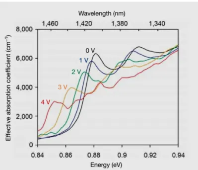
longer wavelengths (red shift). Since electron and hole states shift to opposite sides of the well, overlapping of electron and hole wave functions reduces and it results with the decrease of absorption coefficient and exciton absorption peak. As shown in Figure 2.7 [36], exciton absorption peaks are observed for especially low bias voltages for Ge/SixGe1-x p-i-n MQW structures and
broadening effect reduces since the walls of the wells prevent the exciton from field ionizing.
19
Figure 2.7 Electro-absorption spectra of p-i-n Ge/SiGe MQW structure exploiting QCSE (After Ref. [36])
QCSE has stronger electro-absorption behavior with respect to FKE with thanks to the quantum confinement nature. Excitonic effects are also obvious with respect to FKE, since electrons and holes are confined within the well region. Furthermore, the shape of the wells can be effectively modified with the electric field [38]. Consequently, large
€
ΔEgand
€
Δα can be achieved with
relatively low electric field with respect to FKE. The main expense comes from the requirement of controlled high quality growth and fabrication of p-i-n MQW architectures.
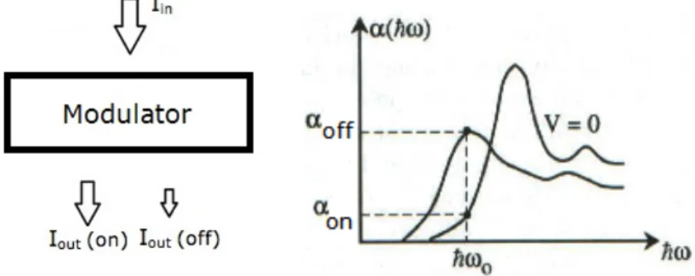
2.2.3 Electro-absorption Modulator Characteristics
An ideal electro-absorption modulator can be conceived as totally transparent to light (“optically on”) for zero bias (E=0) and absorbs all incident light (“optically off”) for particular electric field (E≠0). This section introduces performance metrics for an optical modulator such as contrast ratio, insertion loss and the comprised figure of merit as the performance parameters that should be considered in the design process of an electro-absorption modulator.
20
Figure 2.8 Electro-absorption modulator operation schematic representation
The light intensity between the input and output of the modulator can be related as:
€
I
out ( on,off )= I
in(e
−α( on,off )deff)
(3.11) where €αon,αoff: absorption coefficients for optically “on” and “off” states (
€
αoff >αon),
€
deff: the thickness of MQW region
Contrast ratio (CR): CR is the ratio of the output intensity between optically
“on” and “off” states for a particular electric field, E. Higher applied field implies larger absorption coefficient and less optical power appears at the output of the modulator at the “optically off” state.
CR =
€
I
out(on)
I
out(off )
=€
e
(αoff −αon)deff (3.12)Modulation depth (MD): MD is the performance parameter that refers to the
maximum change in absorption coefficient for particular wavelength and voltage swing. MD =
€
1 −
I
out(off )
I
out(on)
=€
1 − e
−(αoff−αon)deff (3.13)21
Insertion loss (IL): Insertion loss corresponds to the ratio of the input light
intensity to the output at optically “on” state. It is the performance parameter that represents the background material absorption, surface reflections and scattering losses through the modulator in optically “on” state.
IL = € Iin Iout(on) =
€
e
αondeff (3.14)A figure of merit evaluating the optical performance of an electro-absorption modulator with the described performance parameters is defined as:
Figure of merit (FOM) = Contrast ratio (CR) / Insertion loss (IL) (3.15)
For the design of a high performance modulator, FOM should be increased as much as possible. For the achievement of high FOM, absorption coefficient difference (
€
Δα ) and ratio (
€
αoff /αon) for optically “off” and “on” states should
be designed as large as possible. Moreover, absorption coefficient for transparent mode operation (
€
αon) should be minimized to achieve lower
insertion loss.
2.3 SiGe Research Review
This part of the chapter discusses advances in the SiGe optoelectronic device technology summarizing the best-reported results for photodetectors and modulators.
2.3.1 p-i-n Photodetector Literature Review
In the SiGe technology, the main issue tackled in the recent literature is achieving high quality materials. SiGe optoelectronic device technology struggles with the threading dislocations that arise during the growth of epitaxial-Ge layer on Si due to 4.2% lattice mismatch. These threading
22 dislocations affect the carrier transport mechanisms and device parameters such as reducing carrier lifetime and mobility [43] and degrade the device performance in terms of increased dark current and reduced detection efficiency. To date, different research groups demonstrated several growth techniques to reduce the threading dislocations [22-27], as discussed in Chapter 1.
Dark current is a substantial device parameter that dictates the important factors such as power dissipation, signal to noise ratio and noise equivalent power. Low dark current levels are desired to become feasible alternatives to competing III-V based optoelectronic devices [44]. Table 2.1 is a list of the lowest-reported dark current performances and corresponding material growth techniques and other critical device parameters [26], [45-48].
Table 2.1 Reported best dark current performances associated with the growth techniques
Lowest dark current density (1 x 10⁻⁶ A/cm2) is achieved with n-i Ge/p Si configuration [48]. The growth of 1 µm thick Ge epitaxial layer is performed with cyclic thermal annealing using low-energy plasma-enhanced chemical vapor deposition (LEPECVD) system. Cyclic thermal annealing associated with the LEPECVD growth reduces threading dislocation density significantly (~2 x 107 cm-2), hence reducing the dark current. Effect of annealing is obvious, since the same growth without annealing exhibits dark current density of ~2 x 10⁻³ A/cm2. Acquired responsivity values are less than 1 x 10⁻³ A/W at
23
p-type Si layer, which reduces carrier collection efficiency. Low-temperature
molecular beam epitaxy (LT MBE) growth of p-i Ge/n Si configuration exhibits
slightly higher dark current density (2 x 10⁻⁴ A/cm2) with the responsivity of 2 x 10⁻² A/W at 1.3 µm [46]. Other growth techniques such as graded buffer UHCVD, LT/HT UHCVD and LT/HT RPCVD exhibit low dark current with higher detection efficiency performance [26], [45], [47].
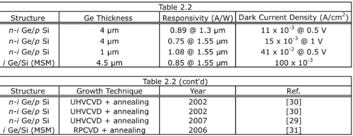
Table 2.2 shows the best-reported SiGe based p-i-n and an extremely efficient MSM photodetector responsivity performances and corresponding parameters.
Table 2.2 Reported best responsivity performances for different device structures
Highest responsivity for top illuminated p-i-n photodetector is reported [30] as 0.89 and 0.75 A/W at 1310 and 1550 nm, respectively. n-type and intrinsic Ge (~4 µm) layers are grown by employing low temperature buffer layer and cyclic thermal annealing using UHVCVD system. Thick intrinsic region is increased the carrier generation. The corresponding dark current densities are 11 and 15 × 10-3 A/cm2 at 0.1and 0.5 V, respectively. Low dark
current exhibits low defect density layers. The integration of photodetectors with waveguides [29] exhibits increase in the detection efficiency. Higher dark current (41 x 10-2 A/cm2 at 0.5 V) is due to large peripheral leakage in waveguide architecture, which dominates for small area devices. High responsivity (1.08 A/W at 1.55 µm) is achieved with low fiber-waveguide coupling loss and waveguide propagation loss. Maximum achievable
24 responsivity is acquired with very low bias [30] (or zero bias [29]) condition, which proves that the built-in electric field across the intrinsic region is sufficient for carrier collection. Highest responsivity (0.85 A/W at 2 V) for a SiGe based MSM photodetector is reported by Okyay et al. [31]. The growth is based on the novel heteroepitaxy technique (MHAH), which enables low dislocation density heteroepitaxial growth of Ge on Si. Measured responsivity values are comparable with the demonstrated p-i-n devices [29-30]. Detailed growth information can be found in the Appendix section.
2.3.2 p-i-n Electro-absorption Modulator Literature Review
Electro-absorption modulator research review covers the best modulation performances based on the modulation mechanisms of Franz-Keldysh [49] and quantum-confined Stark effect [36], [50-51]. All of the configurations include reverse bias operated p-i-n devices associated with the SixGe1-x alloy in the
intrinsic region. Table 2.3 depicts the demonstrated electro-absorption modulators with the corresponding device and performance parameters.
Table 2.3 Reported electro-absorption modulator performances based on FKE [49] and QCSE [36], [50-51]
Researchers at MIT reported a waveguide-integrated p-i-n Si0.08Ge0.92
structure as a high performance electro-absorption modulator exploiting FKE
25 (1530-1565 nm) with the appropriate material composition. Growth is performed with UHVCVD system with cyclic thermal annealing. Silicon waveguides are utilized for light propagation and butt-coupling into and out of
p-i-n device. Absorption for wavelengths longer than 1540 nm is enhanced with
the applied field. Contrast ratio of 10 dB at 1540 nm and 7 V bias, insertion loss of 3.7 dB at 1550 nm is achieved. Modulation depth is increased significantly (85% at 7 V) with the applied voltage higher than 4 V.
A p-i-n device associated with 10 pairs of MQWs (10 nm Ge/16 nm Si0.15Ge0.85) in the intrinsic region exploiting QCSE is demonstrated by research
groups at Stanford University [36]. Growth is performed with RPCVD system with intermediate thermal annealing steps. This work is the very first demonstration of a SiGe MQW electro-absorption modulator with the modulation performance comparable to that of conventional III-V based devices. Electro-absorption operation wavelength is between 1443-1471 nm and further reported for 1550 nm operation at higher temperatures [37]. 4.69 of absorption coefficient ratio (
€
αoff /αon) is achieved at 1461 nm operation.
In 2007, Stanford researchers demonstrated an optical link employing Ge/SiGe MQWs [50-51]. A photodetector and a modulator with 10 nm Ge and 33 nm Si0.16Ge0.84 MQW pairs are connected with SiGe waveguides. The growth
is based on RPCVD growth followed by cyclic thermal annealing to reduce the threading dislocation density. QCSE is exploited with a contrast ratio >3 dB for 1475 – 1497 nm wavelength range and 6 V bias. Photodetectors show responsivity up to 0.26 A/W. This work implies a proof-of-concept demonstration for the integration of photodetectors and modulators to build an optical interconnect.
All of these approaches are promising demonstrations for small footprint, low power and high-speed operation. Furthermore, high electro-absorption performance and Si CMOS compatibility opens a path for integration of electrical and optical circuitry.
26
Chapter 3
Device Fabrication
The epitaxial layers composed of SixGe1-x MQW structures were grown using
Multiple Hydrogen Annealing for Heteroepitaxy (MHAH) [21] technique at Stanford Nanofabrication Facilities (SNF). All of the remaining device fabrication processes are conducted in class 100 and class 1000 facilities at UCF (UNAM clean room facilities) and ARL (Advanced Research Laboratories) at Bilkent University. This chapter details processing steps that are performed for the fabrication of p-i-n photodetector and electro-absorption modulator. Details of layer growth are provided in the Appendix section.
3.1 Substrate and Surface Preparation
MHAH-grown 4” Silicon p-type wafers are cleaved into small pieces and
fabrication is performed on sample pieces. Piece processing reduces the yield however, is preferred in this work due to limited supply of epi-grown-wafers. Epi-grown-wafers are labeled as I18 and I19. Nanostructural characterization information (layer thicknesses, material composition, etc.) is given in Chapter 4. Surface preparation before device fabrication is critical for performance and repeatability. Although the starting substrates are Si, the Ge-rich layers are not compatible with standard RCA cleans. SC-1 and SC-2 cleans attack Ge layers. Therefore, samples are first ultrasonically degreased in acetone ((CH3)2CO), isopropyl alcohol ((CH3)2CHOH) and methanol (CH3OH). Samples
are then rinsed in de-ionized (DI) water and dried by a nitrogen gun. Following the removal of organic contaminants by the previous steps, hydrofluoric acid (HF) cyclic cleaning is performed. Samples are treated in dilute HF (HF(40%):H20=1:50) solution and DI water consecutively and repeated for
27 several times. This clean ensures ultra-clean surface and removes any native oxide layer.
3.2 Patterning
Photolithography process is used to transfer the desired patterns onto the substrate. A photo mask is designed using LayoutEditor (GNU GPL) tool [50]. The mask writing is performed with a Heidelberg Instruments DWL-66 Mask Writer in UCF. A three-mask process is designed with an initial mask layer used to define circular mesa shapes of p-i-n devices with 20 µm to 150 µm diameters. After deposition of a dielectric layer, consequent alignment steps are used to define contact windows in dielectric layer and a final mask to form top and bottom metal electrodes. Test structures for SEM imaging and alignment marks are also included in the designed photomask. Figure 3.1 shows the mask with Chromium (Cr) patterns and the designed patterns in CAD environment.
Figure 3.1 a) Photolithography mask, b) level CAD design of p-i-n structures, c) Multi-level design (closer view), d) Optical micrograph image of metallization lift-off mask
28 Surface de-hydration of samples is performed on a hot plate at 110°C for 5 min. This step removes humidity off the surface, ensuring better and repeatable photoresist coverage as well as improving the resolution of the features. Hexametyldisilazane (HMDS) layer is used to promote photoresist adhesion on the surface. AZ5214E of AZ Electronic Materials photoresist (PR) is spin-coated at 5000 rpm for 50 seconds resulting in 1.3-µm-thick layer. Pre-exposure bake is used to remove solvents in the photoresist. Electronic Vision Group EVG620 Mask Aligner is used for alignment and UV exposure with constant dose (~50 mJ) at all photolithography steps. Post-exposure bake can be used to further improve resolution, but this step was usually skipped, as the minimum feature size in this work was repeatable without this step. AZ400K developer (AZ400K:H20=1:4) is used for the development of the exposed
samples.
3.3 Dry Etching
Dry etching is performed for the definition of p-i-n circular mesa structures using Ultra High Vacuum (UHV) Reactive Ion Etcher (RIE) in ARL. Process development prior to etching process is performed to acquire etch rates for Si, Ge, SixGe1-x and photoresist. Acquiring accurate etch rates are crucial for p-i-n
device fabrications since it is critical to etch down to p-type layer, so the mesa structure contains all n-type, intrinsic and p-type layers successively from top to bottom. PR is used as masking layer and SF6 is used as the process gas. Etch
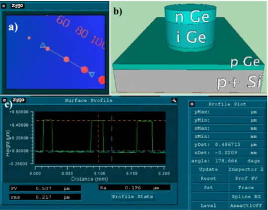
profiles are inspected with DEKTAK stylus profilometer, ZYGO Newview7200 optical profilometer and SEM imaging to ensure the consistency of the projected etch depth and mesa geometry. Figure 3.2 a) shows a top view of an etched sample, each circle corresponding to mesa shapes with different diameters. The planar scanning distance is set prior to measurement. Figure 3.2 b) depicts the schematic representation of the etched sample and c) shows the surface profile with ZYGO optical profilometer. Measured etch depths are ~400 and ~500 nm, for samples I18 and I19, respectively.
29
3.4 Dielectric Film Coating
Dielectric film quality is immensely important for the photodetector fabrication since it is used both as anti-reflection (AR) coating and for electrical surface passivation. High film quality is required for low surface leakage. Besides, conformal deposition of the dielectric material around the mesa shape is crucial for p-i-n mesa structures to make sure that each layer are electrically isolated from each other prior to metallization process in addition to suppress sidewall leakage.
Figure 3.2 a) Top view of the circular mesa structures on ZYGO optical profilometer program, b) Schematic 3D representation of one of the etched samples, c) Scan results of ZYGO optical
profilometer
Conformal deposition of high quality and low stress SixNy is performed
using Plasma Enhanced Chemical Vapor Deposition (PECVD) system. SiH4
(200 sccm) and NH3 (4 sccm) are used as process gases and He (50 sccm) is
used for low stress film deposition. Process development is performed prior to deposition. Process temperature is set to 250°C with the chamber pressure of
30 1 Torr and RF power of 9W. Deposition rate is calculated as 9.3 nm/min and the thicknesses of the deposited SixNy films (~100 nm) are confirmed with J. A.
Woolam V-VASE Ellipsometer.
3.5 Wet Etching
Wet etching is used to form via holes through the SixNy layer in order to contact
p- and n-type layers. SixNy is etched using buffered HF solution
(HF(40%):NH4F(40%)=1:7) and PR is used as masking layer. Process
development is performed prior to etching using test samples. Figure 3.3 a) shows the optical micrograph image and b) shows the schematic representation of the etched sample.
Figure 3.3 a) Optical micrograph image (top view), b) Schematic representation of the etched sample
3.6 Metallization and Electrode Formation
Fabrication of the p-i-n photodetector structures is completed with metallization and the definition of top and bottom (n- and p-type layers, respectively) electrodes. After the last alignment photolithography, an “HF-last” step is performed to ensure oxide free surface. 200-nm-thick aluminum (Al) is evaporated by VAKSIS thermal evaporator with an ultra-thin (~10 nm) layer of Titanium (Ti) in between to enhance the adhesion of Al onto the sample surface. Samples are rotated during evaporation to enable conformal sidewall coverage
31 and also uniform deposition on sample surface. After metallization, samples are left in acetone for lift-off process. Figure 3.4 shows the schematic representation, SEM and optical micrograph image of the final p-i-n mesa structure.
Figure 3.4 a) SEM micrograph image of final p-i-n device and schematic representation (inset), b) Optical micrograph image of devices with different MESA diameters, c) Optical micrograph
32
Chapter 4
Material and Device Characterization
This chapter describes the nanostructural material characterization of grown two different p-i-n SixGe1-x MQW architectures (labeled as I18 and I19) and
optoelectronic device characterization of the fabricated devices. Material
characterization includes Transmission Electron Microscopy (TEM), X-ray photoelectron spectroscopy (XPS), Photoluminescence (PL) and Raman
spectroscopy measurements to acquire material compositional information and ensure the quality of grown layers. Band structures of the grown samples are revealed with the acquired characterization data. Device characterization involves electrical and optical characterization for the demonstration of photodetector and electro-absorption modulator operation.
4.1 Material Characterization
Material growth of the p-i-n MQW structures is performed using a novel heteroepitaxy technique, Multiple Hydrogen Annealing for Heteroepitaxy (MHAH). Growth of the layers used in this thesis is a topic of another study. The details of the growth process can be found in the appendix section. This section presents the nanostructural characterization studies and results obtained.
4.1.1 Nanostructural Characterization
Cross-sectional Transmission Electron Microscopy (TEM) is used to determine the crystal quality of the grown layers in addition to the thickness of alternating well and barrier regions. Figure 4.1 shows TEM images of the grown quantum structures. Epitaxial growth with low defect and threading dislocation density is obtained. Furthermore, strained MQW pairs can be smoothly distinguished with high contrast imaging. Layer thicknesses are extracted from TEM images and are listed in Table 4.1.
33
Figure 4.1 TEM images of p-i-n MQW structures (samples I18 and I19, respectively)
Table 4.1 Layer thicknesses of p-i-n MQW structures (samples I18 and I19)
X-Ray photoelectron spectroscopy (XPS) measures the binding energies of atoms and acquires composition related information about the grown layers. Layer thicknesses of p-i-n and MQW layers with the material compositional information is essential to reveal the heterostructure band diagram and analyze the optoelectronic device operation.
34
Figure 4.2 XPS Study - Concentration profile in terms of depth (sample I19)
The XPS analysis of the layers for Si (Si-2p) and Ge (Ge-3d) binding energies were carried out. The layers are in-situ etched by a secondary beam and scattered energy spectrum is recorded periodically. Samples are etched with a rate of ~0.2 nm/sec and scattered spectrum is recorded at the end of each 8-second interval, as shown in Figure 4.2. The undulating behavior of Si and Ge concentration proceeding from t=600 sec, is due to concentration modulation between barrier (SixGe1-x, x=0.1) and well (Ge) regions. By direct linear
interpolation of direct gap between Si and Ge, n-type Ge cap layer (Si0.05Ge0.95) has an absorption edge which is shorter than 1550 nm (excluding
weak indirect gap absorption). Hence, provides near-transparent behavior around 1550 nm operation range.
Photoluminescence (PL) spectrum is measured to observe the crystalline quality of p-i-n MQW structures and probe available energy states and allowed transitions between the states. PL measurements were obtained by light
35 excitation at
€
λ = 225 nm. The layers have the sharp luminescence peaks at 425 nm and 500 nm, as shown in Figure 4.3. Electroluminescence (EL) measurement is also recorded, however emission peak is not observed attributed to the indirect gap of Ge and thick intrinsic region.
Figure 4.3 Photoluminescence spectra with excitation wavelength of 225 nm (sample I18)
Raman spectroscopy is performed to investigate phonon modes of the system. Typical Raman spectrum of a Ge/SixGe1-x system might involve Ge-Ge,
Ge-Si and Si-Si vibrational modes and depend on the film thickness, stress, material content and quality [52]. The shifted energy of excitation photons of 532 nm gives information about the material composition as shown in Figure 4.4. The penetration depth of such excitation enables us to get information about the Ge and SixGe1-x (x=0.1) layers. Ge-Ge peak (~297) corresponds to the
Raman shift associated with Ge-rich layers. Furthermore, Ge (~385) and Si-Si (~450) peaks represent the Si-Si-Ge and Si-Si-Si-Si bonds of Si-SixGe1-x layers. Peak
![Figure 2.3 p-i-n photodetector operation under illumination (After Ref. [42])](https://thumb-eu.123doks.com/thumbv2/9libnet/6017414.126964/25.892.212.728.194.619/figure-p-photodetector-operation-under-illumination-after-ref.webp)