Low-Frequency Time-Domain Characterization
for Fast and Reliable Evaluation
of Microwave Transistor Performance
Gianni Bosi, Antonio Raffo, Valeria Vadalà,Francesco Trevisan, Giorgio Vannini Department of Engineering
University of Ferrara Ferrara, Italy [email protected]
Omer Cengiz, Ozlem Sen, Ekmel Ozbay Nanotechnology Research Center (NANOTAM)
Bilkent University Ankara, Turkey [email protected]
Abstract—In this paper, we introduce the use of the
low-frequency characterization of electron devices as an accurate and economical way to fast gather consistent data about the electron device performance at microwaves in the evaluation phase of new components, technologies and processes.
Keywords—GaN, HEMT, measurements, semiconductor devices
I. INTRODUCTION
When a new technology is being developed, the fast evaluation of the performance of the fabricated electron devices is a fundamental step for the optimization of the technological process. The same applies when new COTS (Commercial Off-The-Shelf) transistors must be preliminarily evaluated for a specific application.
Conventional characterization techniques, such as load-pull systems, can provide a good overview of the device performance. However, these measurements involve expensive instrumentation and time-consuming procedures, especially when a large amount of devices needs to be characterized. In addition, since they operate at microwaves, some of the most important parameters that determine the device performance (e.g., dynamic knee walkout [1]) or reliability (e.g., Shottky junction dynamic conduction [2]) may be hidden because of the effects of the device parasitic elements and intrinsic capacitances.
In this paper, we show that a suitable low-frequency (LF) characterization of electron devices performed at a few megahertz [1] can provide very useful data about some of the most important indicators, such as output power and efficiency, which are perfectly consistent with the corresponding high-frequency (HF) quantities. Indeed, at LF, we have a direct insight of the current-generator dynamic behavior, with the considerable advantage of monitoring some of the intrinsic quantities hidden at microwaves.
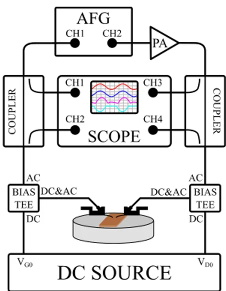
Fig. 1. LF active load-pull measurement setup. II. LOW-FREQUENCY SETUP
The LF setup adopted implements a time-domain active load-pull system operating in the frequency bandwidth [200 kHz – 240 MHz]. It is composed of common laboratory instrumentation, as reported in Fig. 1. The device under test (DUT) is biased by using a conventional DC source. A 2-channel arbitrary waveform generator is used to inject an incident wave at both the gate and drain ports of the DUT. AC and DC components are mixed up by using two bias tees. A 4-channel oscilloscope acquires the DUT incident and reflected waves by means of two bi-directional couplers inserted in the AC paths of the setup. All the instruments are controlled by an in-house developed software, which processes the data acquired by the oscilloscope and shifts their reference planes to the DUT. This is possible because the AC paths of the system are previously characterized by means of their S-parameters within the bandwidth of the setup. This information is then used to accurately tune the amplitude and phase of the injected
978-2-87487-044-6 © 2016 EuMA 3 – 4 Oct 2016, London, UK
Proceedings of the 11th European Microwave Integrated Circuits Conference
incident waves in order to synthetize the desired load conditions at the output port of the DUT.
Since this setup operates at frequencies in the megahertz range, when the DUT is a microwave device we can neglect its reactive effects and therefore observe the behavior of the device current generator. This can be strongly affected by the so-called low-frequency dispersion phenomena, which induce a LF dependence due to the dynamics of the device thermal and trap states. However, as well known, the cut-off frequency for these phenomena is typically below 1 MHz [3, 4], above which the current generator is practically frequency independent. It has been also demonstrated [5] that LF measurements are able to accurately characterize the fast charge capture phenomena typical of GaN technologies. As a consequence, the LF measured data can provide information consistent with the device RF operation.
As an additional advantage of the system, the characterization is performed under continuous wave (CW) regime, which is a more realistic operating condition for microwave devices if compared, for instance, to pulsed I/V measurements.
III. DEVICE TECHNOLOGY
The measurements we report in this paper refer to a 0.25-µm GaN HEMT device with a total gate periphery of 1 mm. The device was fabricated by using the Bilkent University Nanotechnology Research Center (NANOTAM) GaN HEMT process.
The AlGaN/GaN heterostructure was grown on a semi-insulating SiC substrate by using metal organic chemical vapor deposition (MOCVD) in NANOTAM. Firstly, mesa etching was performed to isolate the devices by using ICP-RIE, followed by the formation of ohmic contacts by using Ti/Al/Ni/Au with thicknesses of 12 nm, 120 nm, 35 nm, 65 nm respectively. The ohmic contact resistance was measured as 0.35 Ω·mm. After that, Г-shaped (gamma gate) gate was defined by using electron beam lithography and deposited by using Ni/Au metals. As the next step in process, the devices were passivated by using a 300 nm Si3N4 layer grown by plasma enhanced chemical vapor deposition (PECVD). The last step was forming the air-bridges and the interconnect metallization. A schematic of the Г-gate HEMT structure can be seen in Fig. 2.
IV. LOW-FREQUENCY CHARACTERIZATION
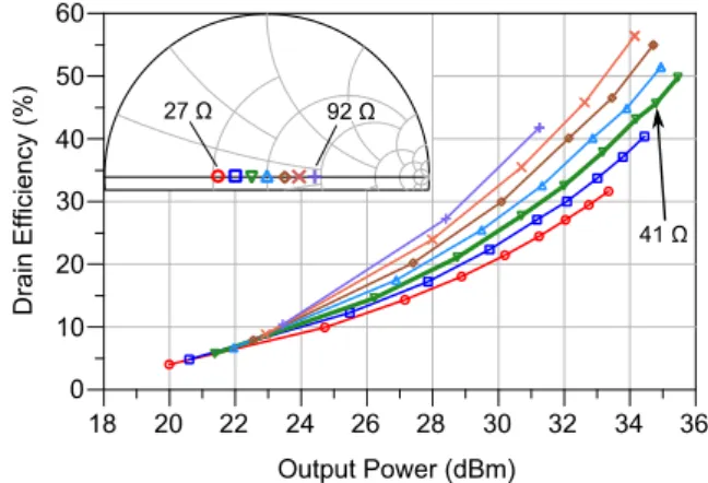
After a conventional characterization step based on DC I/V measurements, we characterized the device by means of the setup in Fig. 1. We chose a bias point for class-AB operation, i.e., VGQ = -3.2 V, VDQ = 25 V, IDQ = 100 mA. A preliminary set of measurements was aimed at evaluating the optimum impedance to be presented at the current-generator plane (CGP) to maximize the output power and efficiency. We performed a power sweep by exciting the input port of the device with a sinusoidal waveform at 2 MHz of variable amplitude from 0.5 to 4.5 V and tuning the output incident wave to actively synthesize a set of seven real impedances, from approximately 27 Ω to 92 Ω. In Fig. 3, we report the
results of the drain efficiency vs the output power for each impedance. The impedance that came out to be the best trade-off is 41 Ω.
Fig. 2. Schematic of the Γ-gate HEMT structure.
Fig. 3. Efficiency vs output power for the set of load impedances reported in the inset. The bold line refers to the impedance which shows the best power/efficiency trade-off.
Note that the automatic control procedure of the setup did not reach the same amount of power levels for each impedance. This puts in evidence a capability of the system: since we operate in time domain with direct access to the current-generator waveforms, we can monitor the dynamic vGD voltage and prevent it to reach values that may stress or, in the worst case, damage the device. Thus, for this first set of LF data, we set the minimum dynamic vGD at -50 V, which explains why the number of measured power levels is lower for the higher impedances.
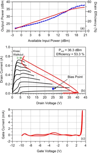
Once the optimum impedance was found, we performed a second power sweep with a finer step for this fixed load to gather more data. They are presented in Fig. 4, where we also show the time-domain load line for the highest power level we have measured, corresponding to an amplitude of the input waveform of 6.8 V. The maximum power obtained was 36.3 dBm (≈ 4.3 W/mm) with a maximum efficiency of 53.3 %. We did not exceed this value since we decided to prevent an excessive conduction of the Schottky junction, which is already clearly visible as reported in Fig. 4c.
Looking at the load line (Fig. 4b), it is also noticeable the phenomenon of the dynamic knee walkout which limits the maximum performance of the device [6].
It is interesting to note that all these data were obtained with a relatively small number of measurements, which implies a reduced amount of time (1 hour), with particular care on the device reliability to avoid an excessive stress or degradation of the device under test.
Fig. 4. Results for the selected optimum impedance: a) output power (solid line) and drain efficiency (dashed line) vs available input power; b) measured load line for maximum power (solid line) and DC I/V characteristics (dashed lines); c) gate I/V locus for the measured maximum power.
TABLE I. LOAD IMPEDANCES AT HFPREDICTED BY NONLINEAR
EMBEDDING
ZL @ CGP Fundamental Frequency ZL @ HF
41 Ω 8 GHz 19.6 + j16.9 Ω
V. COMPARISON WITH HFDATA
In this Section, we compare how the LF data match with RF operation. Even if HF time-domain data were available for the examined transistor, a direct comparison would not be possible since at RF the reactive effects of the device parasitic structures and of the intrinsic capacitance completely mask the current-generator behavior analyzed with the LF setup.
For this reason, we adopted the nonlinear embedding approach [7, 8]. This technique aims to identify the HF condition corresponding to the one measured at LF, ωLF, in terms of extrinsic voltages and currents (and therefore, source and load terminations) at a selected design frequency at microwaves, ωHF.1
In order to impose a load line consistent with the one adopted at LF, the measured voltage phasors at the CGP are shifted at ωHF. Then, by assuming the nonlinear intrinsic capacitance network connected in parallel to the current generator, its contribution at ωHF can be calculated, provided that a model is available (e.g., by nonlinear simulations in a CAD environment). Once all the electrical variables at the intrinsic plane are known at ωHF, a model of the linear extrinsic network can be used to shift all the data to the extrinsic plane of the device. Then, the other quantities of interests at ωHF corresponding to the current-generator behavior measured at ωLF, can be calculated, and in particular the load terminations. The whole procedure can be easily implemented and used for any microwave frequency of interest starting from the same measured load line at LF, provided that the required parasitic elements and intrinsic capacitance models are sufficiently accurate within the bandwidth of interest.
To apply the nonlinear embedding procedure, we first measured the transistor multi-bias S-parameters in a suitable grid of bias conditions of the DC characteristics reported in Fig. 4. From the cold-FET data, we identified the parasitic network of the device using a conventional approach [9, 10]. Then, as the parasitic effects were de-embeddeded from S-parameter data, the bias-dependent intrinsic capacitances were easily calculated [11], obtaining a LUT-based model.
Successively, we have applied the nonlinear embedding technique [7, 8] considering a target frequency in the X band, i.e., 8 GHz, starting from the load line identified from the LF characterization. The corresponding load impedance predicted by the procedure is reported in Table I.
As a next step, we performed scalar load-pull measurements, with the aim of experimentally identifying the optimum impedance at microwaves. To this aim, we used a Focus Microwaves load-pull system whose architecture can be seen in Fig. 5. It consists of a signal generator, a driver amplifier, an input passive block, which includes a directional coupler, an isolator to protect the amplifier from reflected power and a bias-tee for gate biasing, a source tuner, the DUT, a load tuner, an output passive block which includes a bias-tee for drain biasing, an attenuator to prevent any damage to the output power sensor, a directional coupler to connect the spectrum analyzer to measure the output power. Input power is calculated at the DUT input accordingly to the calibration of the input passive block and the source tuner.
Measurements were performed on-wafer at room temperature with the same bias conditions of the LF measurements, i.e., VGQ = -3.2 V, VDQ = 25 V, IDQ = 100 mA. Firstly, load-pull measurements were performed under small-signal conditions, i.e., input power around 0 dBm, to roughly
1 For the sake of brevity, in the following we will use ω
LF and ωHF implicitly referring also to the harmonic content and not just the fundamental frequency.
determine load and source impedances close to the optimum ones. After that, a power sweep was done to determine the input power for the 1-dB compression point of the device. Then, load-pull measurements were performed to optimize the load impedance for maximum output power at the selected input power level.
Fig. 5. Focus Microwaves load-pull measurement setup.
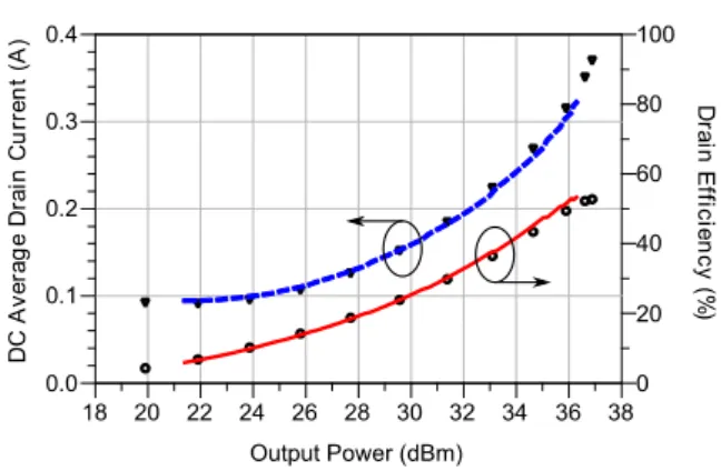
Fig. 6. Comparison between LF measurements at 2 MHz for the identified load impedance of 41 Ω (solid and dashed lines) and HF performance measured at 8 GHz for a load impedance of 19.2 + j23.8 Ω (symbols).
The optimum impedance value for the frequency of 8 GHz was determined as ZL,8 GHz = 19.2 + j23.8 Ω, which is very close to the one predicted by the nonlinear embedding methodology starting from LF measurements.
Some of the data coming from the load-pull measurements can be compared with the ones measured at LF since they are strictly connected to the current-generator behavior. These data are, for example, the output power, the drain efficiency and the average drain current. Therefore, once the optimum impedance was experimentally determined at 8 GHz, we can compare these experimental results with the corresponding LF data, as reported in Fig. 6.
It is remarkable how the LF quantities perfectly fit the corresponding data at microwaves, suggesting that the optimum operation identified at the CGP accurately matches the corresponding one identified directly at 8 GHz, which proves the consistency of the LF characterization. It must be also outlined that HF output power and efficiency data evaluated starting from LF ones through the nonlinear embedding technique differ from the corresponding LF data only due to the additional, slight contribution of the capacitive
current to the power losses of transistor resistive parasitic elements. In the considered case, the difference was just 0.2 dB in output power and 2% in drain efficiency. This further confirms the meaningfulness and consistency of the LF characterization.
VI. CONCLUSION
In this work, we have characterized a GaN HEMT device by means of LF measurements to gather data about its performance. The comparison with the corresponding HF measurements has shown an excellent agreement, proving that quantities as output power and efficiency can be conveniently and accurately estimated also at LF. This aspect, jointly with the possibility of directly monitoring the current-generator dynamic behavior and have access to the intrinsic waveforms, provide a good insight of the device technological quality and can be effectively used by foundries or circuit designers for quick and low-cost process or COTS components evaluation.
REFERENCES
[1] A. Raffo, S. Di Falco, V. Vadalà, and G. Vannini, “Characterization of GaN HEMT low-frequency dispersion through a multiharmonic measurement system,” IEEE Trans. Microw. Theory Tech., vol. 58, no. 9, pp. 2490-2496, September 2010.
[2] A. Raffo, S. Di Falco, G. Sozzi, R. Menozzi, D. Schreurs, and G. Vannini, “Analysis of the gate current as a suitable indicator for FET degradation under nonlinear dynamic regime,” Microelectronics Reliability, vol. 51, no. 2, pp. 235-239, February 2011.
[3] J. Joh and J. A. del Alamo, “A current-transient methodology for trap analysis for GaN high electron mobility transistors,” IEEE Trans. Electron Devices, vol. 58, no. 1, pp. 132-140, January 2011.
[4] R. Riley, “Accounting for dynamic behavior in FET device models,” Microw. Journal, vol. 54, no. 7, pp. 80-86, July 2001.
[5] G. Bosi, A. Raffo, V. Vadalà, and G. Vannini, “A new description of fast charge-trapping effects in GaN FETs,” in IEEE MTT-S International Microwave Symposium (IMS), Phoenix, AZ, USA, 2015, pp. 1-4, May 2015.
[6] S. C. Binari, P. B. Klein, and T. E. Kazior, “Trapping effects in wide-bandgap microwave FETs,” 2002 IEEE MTT-S International Microwave Symposium Digest, vol. 3, pp. 1823–1826, Seattle, WA, USA, June 2002.
[7] A. Raffo, F. Scappaviva, and G. Vannini, “A new approach to microwave power amplifier design based on the experimental characterization of the intrinsic electron-device load line,” IEEE Trans. Microw. Theory Tech., vol. 57, no. 7, pp. 1743-1752, July 2009. [8] J. Haedong, P. Roblin, and X. Zhijian, “Model-based nonlinear
embedding for power amplifier design,” IEEE Trans. Microw. Theory Tech., vol. 62, no. 9, pp. 1986-2002, September 2014.
[9] G. Dambrine, A. Cappy, F. Heliodore, and E. Playez, “A new method for determining the FET small-signal equivalent circuit,” IEEE Trans. Microw. Theory Tech., vol. 36, no. 7, pp. 1151-1159, July 1988. [10] G. Crupi, D. M. M.-P. Schreurs, and A. Caddemi, “On the small signal
modeling of advanced microwave FETs: a comparative study,” International Journal of RF and Microwave Computer-Aided Engineering, vol. 18, no 5, pp. 417-425, September 2008.
[11] D. E. Root, “Nonlinear charge modeling for FET large-signal simulation and its importance for IP3 and ACPR in communication circuits,” Proceedings of the 44th IEEE Midwest Symposium on Circuits and Systems, Dayton, OH, USA, vol. 2, pp. 768-772, August 2001.