Quantum Dot Light-Emitting Diode with Quantum Dots Inside the
Hole Transporting Layers
Kheng Swee Leck,
†Yoga Divayana,
†,‡Dewei Zhao,
†Xuyong Yang,
†Agus Putu Abiyasa,
†Evren Mutlugun,
†,⊥Yuan Gao,
†Shuwei Liu,
†Swee Tiam Tan,
†Xiao Wei Sun,*
,†,∥and Hilmi Volkan Demir*
,†,§,⊥†LUMINOUS! Centre of Excellence for Semiconductor Lighting and Displays, School of Electrical and Electronic Engineering,
Nanyang Technological University, Nanyang Avenue, Singapore 639798, and§School of Physical and Mathematical Sciences, Nanyang Technological University, Nanyang Avenue, Singapore 639798
‡School of Electrical Engineering, Udayana University, Kampus Bukit Jimbaran, Bali, Indonesia
⊥Department of Electrical and Electronics Engineering, Department of Physics, UNAM−Institute of Materials Science and
Nanotechnology, Bilkent University, Bilkent, Ankara, Turkey 06800
∥South University of Science and Technology of China, Shenzhen, Guangdong, China 518055
*
S Supporting InformationABSTRACT: We report a hybrid, quantum dot (QD)-based, organic light-emitting diode architecture using a noninverted structure with the QDs sandwiched between hole transporting layers (HTLs) outperforming the reference device structure implemented in conventional noninverted architecture by overfive folds and suppressing the blue emission that is otherwise observed in the conventional structure because of the excess electrons leaking towards the HTL. It is predicted in the new device structure that 97.44% of the exciton formation takes place in the QD layer, while 2.56% of the excitons form in the HTL. It is found that the enhancement in the external quantum efficiency is mainly due to the stronger confinement of exciton formation to the QDs.
KEYWORDS: quantum dots, hybrid OLEDs, exciton, electroluminescence, hole transport layer, noninverted structure
1. INTRODUCTION
Organic semiconductors have been exploited in numerous applications including light-emitting diodes (LEDs),1thin-film transistors,2,3 memristors,4 spintronics,5,6 and photovoltaics.7,8 Such a wide range of applications indicate their versatile characteristics. Organics form a class of soft-matter semi-conductors that can favorably be processed at low temper-atures. They can be conveniently deposited onto a variety of low-cost and large-area substrates including thin-film plastics, glasses, and metal foils, which require no lattice matching unlike inorganic semiconductor crystals. Similar to organic semi-conductors, colloidal inorganic semiconductor quantum dots (QDs), also known as nanocrystals, have recently gained popularity. The robustness of these inorganic semiconductor nanocrystals and their capability to tune the electronic structure
and optical properties, again similar to the organics, through structural modifications (for example, in size and composition) are among their main advantages.9Besides, these nanocrystals are capped with organic ligands that make them dispersible in aqueous/organic solutions. Therefore, they can be integrated easily into the conventional organic LEDs (OLEDs) with the use of common low-cost techniques such as spin-coating,10,11 dip-coating,12 layer-by-layer assembly,13,14 inkjet printing,15 contact printing,16 and mist deposition.17 The hybrid combination of organic semiconductors and inorganic nano-crystal colloids potentially allows for new possibilities to control
Received: March 12, 2013 Accepted: June 3, 2013 Published: June 3, 2013
exciton formation, hence achieving high light-emission efficiency.
Significant progress has been made following the first report of QD-LEDs.12The improvements, which mainly result from the efforts of introducing advanced deposition methods,14,18 better device architectures16,19,20and materials,21−26have led to QD-LEDs with a maximum brightness reported of over 10000 cd m−2,24,27,28 and a maximum external quantum efficiency (EQE) of more than 2.7% (peak wavelength around 600 nm).29 To date, most hybrid devices sandwich the QD layer between the hole and electron transporting layers. In such a device design, the electron and hole are expected to form an exciton and recombine inside the QDs. However, the energy band of the QDs favors electron injection more than hole injection. Thus, the exciton formation is inefficient as only a small fraction of holes are able to overcome the large energy barrier to the QDs, whereas most of the electrons leak toward the organic layer, thus resulting in low efficiency device.
In this work, we show that the QDs deposited inside the hole transporting layer (HTL) substantially enhances the device performance in non-inverted device structure. Compared to the conventional device, this proposed architecture yields over five-fold enhancement in EQE in the best device. The improvement was attributed to the stronger confinement of exciton formation in the QDs and the better balance of electron and hole
injection into the QDs. It was also discovered that the Förster resonance energy transfer (FRET) from the HTL to the QDs is minimum in this device architecture. The best device reaches an EQE level of 3.14% with a minimal efficiency droop at the emission peak of 512 nm. To the best of our knowledge, this is the highest reported value for noninverted structures.16,24,29,30
2. EXPERIMENTAL SECTION
QD Synthesis and Purification. Details of the synthetic method of alloyed CdSeZnS quantum dots with a composition gradient are described in the literature.14,31 For a typical preparation of green-emitting QDs, 0.1 mmol of cadmium oxide (CdO), 4 mmol of zinc acetate (Zn(Acet)2), 5 mL of oleic acid (OA), and 20 mL of
1-octadecene (1-ODE) were loaded in a 50 mL 3-neckflask and heated at 100 °C under vacuum environment to form cadmium oleate (Cd(OA)2) and zinc oleate (Zn(OA)2). The reactor was thenfilled
with nitrogen and heated up to 300°C. At the elevated temperature, 2 mL of tri-n-octylphosphine (TOP) with 0.1 mmol of selenium (Se) and 3 mmol of sulphur (S) was injected into theflask swiftly, and the reaction mixture was maintained at 300 °C for 10 min for the nanocrystals growth. The reactor was cooled to room temperature to complete the reaction, forming alloyed CdSeZnS quantum dots with a composition gradient.
The crude nanocrystals solution was purified by precipitation using acetone and methanol and re-dispersing in toluene. This process was repeated for 3 times, following the redispersion of the QDs in fresh toluene with a concentration of 10 mg/mL for further use. The Figure 1.(a) Device architecture schematics and (b) energy diagram of the devices studied here. In the conventional structure, the quantum dots are sandwiched between the hole and electron transport layers (left), and in the proposed device architecture, the quantum dot layer is sandwiched between two hole transport layers (right).
purified QDs solution was measured to give a quantum yield around 50% in solution by comparing the fluorescence intensities with a standard reference dye,fluorescein-27, which has an emission peak at 502 nm and afluorescence quantum yield of 0.87 in 0.1 M NaOH solution. Furthermore the quantum efficiency value has been confirmed with an independent method (see Figure S1 in the Supporting Information).
Device Fabrication. For the device fabrication, a routine cleaning procedure, including ultrasonication in acetone and ethanol, followed by rinsing in deionized (DI) water, was first carried out to clean patterned indium tin oxide (ITO) glass, which has a sheet resistance of 30Ω/sq. Subsequently, the cleaned substrates were dried in an oven at 80°C. A 5 min O2plasma treatment was applied to the ITO substrates
before they were loaded into the glove box and vacuum chamber for deposition. A layer of poly(3,4-ethylenedioxythiophene)-poly-(styrenesulfonate) (PEDOT:PSS) was spin-coated at 3000 rpm and baked in N2 atmosphere for 30 min, followed by 30 nm of
poly(4-butylphenyl-diphenyl-amine) (poly-TPD) serving as the HTL. The QD emissive layer was spin-coated at a speed of 2000 rpm and annealed at 150°C under N2environment for 30 min. On top of the
QD layer, the hole transport layer (4,4′,4′′-tris-(carbazol-9-yl)-triphenylamine (TCTA), 4′-bis(carbazol-9-yl)-biphenyl (CBP), 4-butylphenyl-diphenyl-amine (TPD), or N,N′-bis-(1-naphthyl)-N,N′′-diphenyl-1,1′-biphenyl-4,4′-diamine (NPB)), 1,3,5-tris(N-phenylben-zimidazol-2-yl)benzene (TPBi), lithiumfluoride (LiF), and aluminum (Al) were deposited by thermal evaporation. The effective area of the LED devices is 9 mm2.
Measurements. UV−vis absorption spectra were measured with Shimadzu UV-2450 spectrophotometer, fluorescence measurements were obtained with Horiba Jobin Yvon Fluorog-3 FluorEssence spectrofluorometer and the photoluminescence quantum yield of the QDs was determined by comparing with the standard reference dye by the reported method.32
The electroluminescence (EL) spectra of the fabricated OLEDs were measured using a PhotoResearch SpectraScan PR705 spectror-adiometer, whereas the electrical characteristics were obtained using Yogakawa GS610 source measurement unit. We assumed the emission pattern was Lambertian, and calculated the EQE from the luminance, current density, and electroluminescence spectrum. All measurements were carried out at room temperature under ambient atmosphere without any encapsulation.
3. RESULTS AND DISCUSSION
Figure 1a shows the schematic of the conventional and improved QD devices with their corresponding band diagrams. The structure of a conventional QD device consists of glass substrate/ITO/PEDOT:PSS/poly-TPD/QDs/TPBi/LiF/ Al.16,27,29,30 In the conventional QD device, poly-TPD and TPBi are used to transport holes and electrons, respectively. The electrons and holes are expected to recombine radiatively inside the QD layer. However, a large highest occupied molecular orbital (HOMO) energy barrier of 1.9 eV exists for the hole to transport toward the QDs. In contrast, the
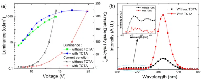
well-Figure 2.(a) L−V and J−V characteristics of the QD devices with TCTA hole transport layer. (b) Electroluminescence spectra of the devices under a current density of 22.22 mA cm‑2(inset) zoom-in of the blue window of the spectrum.
Figure 3.(a) Current density and (b) external quantum efficiency versus voltage characteristics for the devices with varying the thickness of TCTA used as the hole transporting layer. EQE of the devices increases consistently with the addition of TCTA.
aligned lowest unoccupied molecular orbital (LUMO) of TPBi and the conduction band of the QDs do not block the electron transport. This band alignment makes electron injection easier than the hole injection. However, this leads to undesirable exciton recombination outside the QDs. Furthermore, the excess electrons accumulate inside the QDs causing them to charge (QD charging), which increases the Auger recombina-tion rate. To address the charge imbalance issue, slowing down the electron injection rate is necessary. In our study, various HTLs are used to slow down the electron because of their low electron mobility. For the improved device, the HTL is deposited between the QD and electron transport layers as shown in Figure 1a.
Figure 2a shows the J−V and L−V for the conventional and improved QD devices using a well-known TCTA as a HTL to block the electrons. The turn-on voltages are 6.1 and 6.5 V, and the resulting maximum brightness levels are 283 and 10110 cd cm−2for the devices without and with TCTA, respectively. The electroluminescence spectrum of the fabricated QD-LEDs is recorded under a current density of 22.2 mA cm−2 and a significant improvement of the QD-LED performance is observed from the device with the TCTA HTL (Figure 2b). Compared to the conventional device, more than 5-fold enhancement in the brightness can be obtained when the QD layer is sandwiched between the two HTLs (poly-TPD and TCTA). In addition, the improved QD device also suppresses the blue emission that is otherwise observed in the conven-tional structure (inset of Figure 2b). This blue emission is attributed to the poly-TPD layer, which clearly shows that excess electrons leak towards the HTL and recombine with the holes outside the QDs. Therefore, it can be safely concluded that the deposition of TCTA can reduce the electrons injected into QDs and result in a better charge balance in the QD layer, which agrees with our previous assumption.
To further investigate the effect of TCTA on the device performance, we fabricated a series of devices with different TCTA thicknesses. Figure 3a shows the current density versus of the device voltage with different TCTA film thicknesses. Under the same current density, the operational voltage increases with the TCTA thickness, mainly due to the low electron conductivity of TCTA (<1× 10⁻⁸cm2V−1s−1)33
and the energy barrier at the TPBi/TCTA interface. Figure 3b presents the EQE versus current density for the devices given in Figure 3a. The EQE of the conventional device (without TCTA) is also depicted in the samefigure. It can be clearly seen that 20 nm thick TCTA gives the best device performance and the observed efficiency droop (EQE roll-off) is comparable to the previous literature.16 This suggests that the charge balance was optimized at 20 nm. The maximum achievable brightness is 26370 cd m−2under the current density of 333 mA cm−2. The highest EQE, current efficiency and power efficiency achieved in this structure are 3.14%, 8.7 cd A−1and
4.4 lm W−1, respectively, whereas these are only 0.59%, 1.7 cd A−1, and 0.8 lm W−1, respectively, for the conventional device under the same current density.
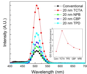
We then investigated the effects of other HTLs on the device performance. Three commonly used HTL, CBP, NPB, and TPD, were used in this study and the devices emission spectra are shown in Figure 4. The inset of Figure 4 presents the enhancement factor (the number of fold enhancement) in the QD emission compared with the conventional QD-LED structure. The devices with QDs sandwiched between HTLs consistently exhibit improvement in EQE. Comparing between
four sets of devices, the device with TCTA outperformed those with other HTL devices. NPB, TPD, and CBP have much higher electron mobility (6× 10⁻⁴, 9× 10⁻⁴, and 3× 10⁻⁴cm2 V−1s−1, respectively)33−35than the TCTA (<1× 10⁻⁸cm2V−1
s−1). For a device using these three HTLs, more electrons can be injected into the QDfilm because of their higher electron mobility. Therefore, the charge balance could not be optimized in the QD layer, hence yielding low device performance.
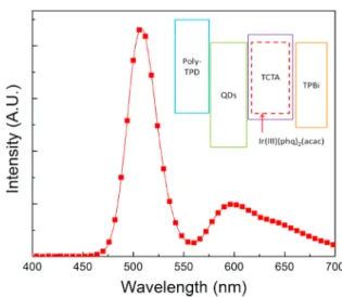
Beside the effect of charge balance, QDs are also playing an important role in the device performance. QDs, without sufficient surface passivation, contain inherent dangling bonds which can trap both electrons and holes. Long hydrocarbon chains with functional groups of phosphine, carboxylic acid, and thiol are attached on the surface of QDs to passivate the surface and reduce the dangling bonds but it is still difficult to cover the QDs’ surface completely. Therefore, direct exciton formation inside QDs will be inefficient even if the charge is well balanced in the QD layer. The improvement in the device performance observed here may also possibly be attributed to the exciton formation in the organic semiconductor (i.e., TCTA, NPB, TPD, or CBP) combined with nonradiative energy transfer to the QDs.16 To understand the factors causing the improve-ment, we used a phosphorescence organic molecule, bis(2-phenylquinoline)(acetylacetonate)iridium(III) (Ir(III)-(phq)2(acac)), to study the exciton distribution inside the
device. The devices fabricated in this study consisted of ITO (150 nm)/PEDOT:PSS (60 nm)/poly-TPD (30 nm)/QD emissive layer (20 nm)/TCTA: Ir(III)(phq)2(acac) (5%, 20 nm)/TPBi (35 nm)/LiF (0.5 nm)/Al (150 nm), in which Ir(III)(phq)2(acac) is used to harvest all the exciton forming in the TCTA layer. Figure 5 shows the emission spectra of the corresponding devices with the sensing layer inside TCTA layer under current density of 22.22 mA cm−2. The emission spectra are from the QD and Ir(III)(phq)2(acac) molecule with the emission peaks at 512 and 596 nm, respectively. It is observed that QDs make more contribution in the emission. The deconvolution study predicts that 97.44% of the exciton formation is in the QD layer, while only 2.56% of the excitons formed in the TCTA layer. In addition, it is also found that the energy transfer from the organic transport layer to QDs has been miniscule in our study and the enhancement in EQE is
Figure 4. Electroluminescence spectra of the devices using different hole transport layers and (inset) enhancement factor achieved in the QD emission using different HTL compared with the conventional structure. The emission spectra were recorded under the same current density of 1 mA cm−2.
mainly due to the improvement of charge balance in the system. We then used the same principle to fabricate hybrid devices with QDs of different sizes. The devices with QDs sandwiched between the HTLs consistently outperform the control devices. Here we achieved four-fold improvement in the blue-emitting device, andfive-fold improvement in the green-and red-emitting device.
4. CONCLUSION
In conclusion, high-efficiency hybrid QD-LEDs have been demonstrated in which the QD active layer is sandwiched inside the hole transporting layer. The best luminance and EQE presented here exhibit more than five-fold enhancement compared to the conventional structure. The improvement is mainly due to the better confinement of the exciton formation in the QDs and the balanced charge carrier injection into the QDs active layer, whereas the energy transfer between the organic layer and QDs in this architecture is minimized. The results indicate that the proposed device architecture with active QDs placed inside the hole transporting layers in this work opens up a simple, efficient pathway to fabricate high-performance QD-based optoelectronic devices.
■
ASSOCIATED CONTENT*
S Supporting InformationIn-film and in-solution quantum efficiency measurement of alloyed CdSeZnS quantum dots with a composition gradient. This material is available free of charge via the Internet at http://pubs.acs.org/.
■
AUTHOR INFORMATIONCorresponding Author
*E-mail: [email protected] (H.V.D.); exwsun@ntu. edu.sg (X.W.S.).
Notes
The authors declare no competingfinancial interest.
■
ACKNOWLEDGMENTSThis work is supported by the National Research Foundation of Singapore under Grant No. NRF-CRP-6-2010-2 and NRF-RF-2009-09 and the Singapore Agency for Science, Technology
and Research (A*STAR) SERC under Grant 112 120 2009 and 092 101 0057.
■
REFERENCES(1) Forrest, S. R. Nature 2004, 428, 911−918.
(2) Gundlach, D. J.; Lin, Y. Y.; Jackson, T. N.; Nelson, S. F.; Schlom, D. G. IEEE Electron Device Lett. 1997, 18, 87−89.
(3) Gelinck, G.; Heremans, P.; Nomoto, K.; Anthopoulos, T. D. Adv. Mater 2010, 22, 3778−3798.
(4) Ouyang, J.; Chu, C.-W.; Szmanda, C. R.; Ma, L.; Yang, Y. Nat. Mater 2004, 3, 918−922.
(5) Xiong, Z. H.; Wu, D.; Valy Vardeny, Z.; Shi, J. Nature 2004, 427, 821−824.
(6) Sanvito, S. Chem. Soc. Rev. 2011, 40, 3336−3355.
(7) Hagfeldt, A.; Gratzel, M. Acc. Chem. Res. 2000, 33, 269−277. (8) Thompson, B. C.; Frechet, J. M. J. Angew. Chem., Int. Ed. 2008, 47, 58−77.
(9) Talapin, D. V.; Lee, J.-S.; Kovalenko, M. V.; Shevchenko, E. V. Chem. Rev. 2009, 110, 389−458.
(10) Hikmet, R. A. M.; Chin, P. T. K.; Talapin, D. V.; Weller, H. Adv. Mater 2005, 17, 1436−1439.
(11) Lee, H.; Kang, C.-M.; Park, M.; Kwak, J.; Lee, C. ACS Appl. Mater. Interfaces 2013, 5, 1977−1981.
(12) Colvin, V. L.; Schlamp, M. C.; Alivisatos, A. P. Nature 1994, 370, 354−357.
(13) Cho, J.; Char, K.; Hong, J. D.; Lee, K. B. Adv. Mater. 2001, 13, 1076−1078.
(14) Bae, W. K.; Kwak, J.; Lim, J.; Lee, D.; Nam, M. K.; Char, K.; Lee, C.; Lee, S. Nano Lett. 2010, 10, 2368−2373.
(15) Derby, B. Annu. Rev. Mater. Res. 2010, 40, 395−414.
(16) Anikeeva, P. O.; Halpert, J. E.; Bawendi, M. G.; Bawendi, M. G. Nano Lett. 2009, 9, 2532−2536.
(17) Price, S. C.; Shanmugasundaram, K.; Ramani, S.; Zhu, T.; Zhang, F.; Xu, J.; Mohney, S. E.; Zhang, Q.; Bawendi, M. G.; Bawendi, M. G. Semicond. Sci. Technol. 2009, 24, 105024.
(18) Kim, T.-H.; Cho, K.-S.; Lee, E. K.; Lee, S. J.; Chae, J.; Kim, J. W.; Kim, D. H.; Kwon, J.-Y.; Amaratunga, G.; Lee, S. Y.; Choi, B. L.; Kuk, Y.; Kim, J. M.; Kim, K. Nat. Photonics 2011, 5, 176−182.
(19) Cheng, K.-Y.; Anthony, R.; Kortshagen, U. R.; Holmes, R. J. Nano Lett. 2011, 11, 1952−1956.
(20) Anikeeva, P. O.; Madigan, C. F.; Halpert, J. E.; Bawendi, M. G.; Bulović, V. Phys. Rev. B 2008, 78, 085434.
(21) Cho, K.-S.; Lee, E. K.; Joo, W.-J.; Jang, E.; Kim, T.-H.; Lee, S. J.; Kwon, S.-J.; Han, J. Y.; Kim, B.-K.; Choi, B. L.; Kim, J. M. Nat. Photonics 2009, 3, 341−345.
(22) Tan, Z.; Zhang, F.; Zhu, T.; Xu, J.; Wang, A. Y.; Dixon, J. D.; Li, L.; Zhang, Q.; Mohney, S. E.; Ruzyllo, J. Nano Lett. 2007, 7, 3803− 3807.
(23) Sun, Q.; Wang, Y. A.; Li, L. S.; Wang, D.; Zhu, T.; Xu, J.; Yang, C.; Li, Y. Nat. Photonics 2007, 1, 717−722.
(24) Qian, L.; Zheng, Y.; Xue, J.; Holloway, P. H. Nat. Photonics 2011, 5, 543−548.
(25) Black, R. Lighting the key to energy saving http://news.bbc.co. uk/2/hi/science/nature/5128478.stm (accessed Feb 14, 2013).
(26) Yang, X.; Zhao, D.; Leck, K. S.; Tan, S. T.; Tang, Y. X.; Zhao, J.; Demir, H. V.; Sun, X. W. Adv. Mater 2012, 24, 4180−4185.
(27) Kwak, J.; Bae, W. K.; Lee, D.; Park, I.; Lim, J.; Park, M.; Cho, H.; Woo, H.; Yoon, D. Y.; Char, K.; Lee, S.; Lee, C. Nano Lett. 2012, 12, 2362−2366.
(28) Shen, H.; Wang, S.; Wang, H.; Niu, J.; Qian, L.; Yang, Y.; Titov, A.; Hyvonen, J.; Zheng, Y.; Li, L. S. ACS Appl. Mater. Interfaces 2013, 5, 4260−4265.
(29) Panzer, M. J.; Aidala, K. E.; Anikeeva, P. O.; Halpert, J. E.; Bawendi, M. G.; Bulović, V. Nano Lett. 2010, 10, 2421−2426.
(30) Bae, W. K.; Kwak, J.; Park, J. W.; Char, K.; Lee, C.; Lee, S. Adv. Mater 2009, 21, 1690−1694.
(31) Bae, W. K.; Char, K.; Hur, H.; Lee, S. Chem. Mater. 2008, 20, 531−539.
Figure 5. Emission spectrum of the device by placing organic phosphorescent molecule in the TCTA layer. This emission spectrum was recorded under the current density of 22.22 mA cm−2. Energy band diagram of the device in this study (inset).
(32) Grabolle, M.; Spieles, M.; Lesnyak, V.; Gaponik, N.; Eychmuller, A.; Resch-Genger, U. Anal. Chem. 2009, 81, 6285−6294.
(33) Kang, J.-W.; Lee, S.-H.; Park, H.-D.; Jeong, W.-I.; Yoo, K.-M.; Park, Y.-S.; Kim, J.-J. Appl. Phys. Lett. 2007, 90, 223508.
(34) Tse, S. C.; Kwok, K. C.; So, S. K. Appl. Phys. Lett. 2006, 89, 26210.
(35) Klenkler, R. A.; Voloshin, G. J. Phys. Chem. C 2011, 115, 16777−16781.