a dissertation submitted to
the department of physics
and the institute of engineering and science
of bilkent university
in partial fulfillment of the requirements
for the degree of
doctor of philosophy
By
Feridun Ay
August, 2005
Prof. Dr. Atilla Aydınlı (Supervisor)
I certify that I have read this thesis and that in my opinion it is fully adequate, in scope and in quality, as a dissertation for the degree of doctor of philosophy.
Prof. Dr. Ra¸sit Turan
I certify that I have read this thesis and that in my opinion it is fully adequate, in scope and in quality, as a dissertation for the degree of doctor of philosophy.
Assoc. Prof. Dr. Recai Ellialtıo˘glu
Assist. Prof. Dr. Hilmi Volkan Demir
I certify that I have read this thesis and that in my opinion it is fully adequate, in scope and in quality, as a dissertation for the degree of doctor of philosophy.
Assist. Prof. Dr. D¨on¨u¸s Tuncel
Approved for the Institute of Engineering and Science:
Prof. Dr. Mehmet B. Baray Director of the Institute
CHARACTERIZATION, AND APPLICATIONS IN
INTEGRATED OPTICS
Feridun Ay PhD in Physics
Supervisor: Prof. Dr. Atilla Aydınlı August, 2005
In recent years, growing attention has been paid to silicon based dielectrics, such as silicon oxynitrides, silicon nitrides, and semiconductor doped silicon oxides, all combined under the name silica on silicon technology. This attention has been motivated mainly due to their excellent optical properties such as well controlled refractive index and high transparency over a wide range of wavelength.
In accordance with the main goal of this study that relied on the utilization of silicon based dielectrics and their optimization for applications in integrated op-tics, an emphasis was given to optimize the compositional and optical properties of these materials. A detailed quantitative compositional analysis using Fourier transform infrared spectroscopy resulted in identification of the germanosilicate dielectrics as the most promising candidates for use in integrated optics. The first reported systematic study of propagation losses for different-index planar waveguides by using prism coupling method was correlated with the composi-tional analysis. This study had an important outcome for planar waveguides fabricated with germanosilicate core layers resulting in the lowest propagation loss values reported so far for as deposited CVD-grown films at λ=1.55 µm, elim-inating the need for costly and cumbersome annealing process.
An improvement of the prism coupling technique led to a new approach for elasto-optic characterization of thin polymer films. This completely new method allows one to determine the optical anisotropy and out-of-plane mechanical prop-erties and to correlate both in order to obtain the elasto-optical propprop-erties of thin polymer films, for the first time.
Of interest as potential electro-optic material, we have concentrated on ther-mally poled germanosilicate films deposited on fused-silica substrates by PECVD.
As a result of an optimization study, we demonstrated a record peak nonlinear coefficient of ∼1.6 pm/V, approximately twice as strong as the highest reliable value reported in a thermally poled fused silica glass.
Finally, we have demonstrated several applications of this technology in the field of integrated optics. Since optical waveguides constitute the building blocks of many integrated optical devices, we had first concentrated on design and opti-mization of waveguides employing germanosilicates as the core layers. The final step of our work concentrated on design and implementation of microring res-onator devices based on germanosilicate layers.
Keywords: Integrated optics, Silicon dielectrics, Silicon oxide, Silicon oxynitride,
Germanium, Germanosilicate, PECVD, FTIR, Waveguide, Optical absorption, Prism coupling, Elastic modulus, Elasto-optic coefficient, Birefringence, Nonlin-earity, Electro-optic coefficient, Thermal poling, Ring resonator.
S˙IL˙ISYUM TABANLI D˙IELEKTR˙IKLER: T ¨
UMLES¸˙IK
OPT˙IKTE KULLANIMA Y ¨
ONEL˙IK B ¨
UY ¨
UTME VE
˙INCELEME
Feridun Ay Fizik, DoktoraTez Y¨oneticisi: Prof. Dr. Atilla Aydınlı Aˇgustos, 2005
Silisyum tabanlı dielektriklerin ¨ust¨un optik ¨ozellikleri ve kırılma indislerinin geni¸s aralıkta ayarlanabilirli˘gi bu malzemelerin t¨umle¸sik optikte kullanılmasına y¨onelik ¸calı¸smalarda b¨uy¨uk ilgi ¸cekmesine neden olmaktadır.
Bu ¸calı¸smada silisyum tabanlı dielektriklerin tumle¸sik optik aygıtlarda kul-lanımları ama¸clanarak optik ¨ozellikleri ve kompozisyonları incelenip optimize edildi. Fourier d¨on¨u¸s¨uml¨u spektroskopi kullanılarak yapılan ayrıntılı kom-pozisyon analazi sonucunda germanosilikat dielektrikleri t¨umle¸sik optik uygula-maları i¸cin en uygun malzemeler olarak tespit edildi. Prizma ¸ciftlemesi y¨ontemi ile germanosilikat d¨uzlemsel dalga kılavuzlarında ilk defa farklı kırılma indisli malzemeler i¸cin kar¸sıla¸stırmalı optik kayıp ¨ol¸c¨umleri yapıldı. Bu ¸calı¸sma net-icesinde literat¨urde ısıl olarak tavlanmamı¸s λ = 1.55 µm dalga boyunda en d¨u¸s¨uk kayıplı duzlemsel dalga kılavuzları elde edildi.
Prizma ¸ciftlemesi tekni˘ginin geli¸stirilmesi ile polimerler gibi yumu¸sak malzemelerin elesto-optik ¨ozelliklerinin ¨ol¸c¨ulebilmesi sa˘glanmı¸stır. Bu yeni y¨ontem ile e¸szamanlı olarak yapılan farklı y¨onl¨u optik indis ¨ol¸c¨umleri ve dikey y¨onl¨u mekanik sabit ¨ol¸c¨umleri kullanılarak, ince polimer tabakaların elasto-optik katsayıları bulunabilmi¸stir.
Germanosilikat dielektriklerinin electro-optik ¨ozelliklerini arttırmak hedefi ile PECVD y¨ontemi ile yapılan b¨uy¨utme ko¸sulları ile ısıl kutuplama ¸sartları optimize edildi. Bunun sonucunda ¸su ana kadar silika cam tabanlı malzemelerde edilmi¸s do˘grusal olmayan en b¨uy¨uk katsayının iki katı elde edildi.
Son olarak, germanosilikatlara dayalı t¨umle¸sik optik aygıtlar ¨uretildi. Bunlar vi
arasında ilk olarak tek kipli dalga kılavuzları ¨uretilip incelendi. C¸ alı¸smanın so-nunda germanosilikatlara dayalı halka ¸cınna¸c aygıtları tasarlandı, optimizasyon ¸calı¸smasını m¨uteakip ¨ozellikleri ¨ol¸c¨uld¨u.
Anahtar s¨ozc¨ukler : T¨umle¸sik optik, Silisyum dielektrikler, Silisyum oksit,
Sil-isyum oksinitrat, Germanium, Germanosilikat, PECVD, FTIR, Dalga Kılavuzu, Optik so˘gurma, Prizma ¸ciftlemesi, Elastik katsayı, Elasto-optik katsayı, Do˘grusal olmayan katsayı, Electro-optik katsayı, Isıl tavlama, Halka ¸cınla¸c.
It is my pleasure to express my deepest gratitude to Prof. Dr. Atilla Aydınlı for his guidance, moral support, friendship and assistance during this research. I am indebted for his efforts and enthusiasm.
I would like to thank the members of my thesis committee: Prof. Dr. Ra¸sit Turan, Assoc. Prof. Dr. Recai Ellialtıo˘glu, Assist. Prof. Dr. Hilmi Volkan Demir, and Assist. Prof. Dr. D¨on¨u¸s Tuncel, for reading the manuscript and commenting on the thesis.
I would like to thank our current and former group members Dr. Aykutlu Dˆana, A¸skın Kocaba¸s (miralay), Co¸skun Kocaba¸s, ˙Isa Kiyat, Or¸cun Erg¨un and Selcen Aytekin for creating a fruitful, enjoyable, and unique working environment. I would like to acknowledge Aydo˘gan ¨Ozcan, M.J.F. Digonnet, and G.S. Kino of Edward L. Ginzton Laboratory, Stanford University, for the close and fruitful collaboration on poled germanosilicates project. Especially the enthusiasm of Aydo˘gan has been a source of motivation for me.
I would like to thank Assoc. Prof. Sedat A˘gan for providing the TEM results along with being so highly motivated and hard working. Our close work with him has been a stimulating experience. I also would like to acknowledge Dr. Temel H. B¨uy¨uklimanlı for providing us with SIMS results. I appreciate the help of the physicist Murat G¨ure and the technician Erg¨un Karaman.
M. Ali Can, ¨Ozg¨ur C¸ akır, Kerim Savran, S¨uleyman U. Eker, Sefa Da˘g, and many other friends helped to keep my spirits high all the time which I appreciate very much.
I am indebted to my family for their continuous support, care, and encour-agement.
And finally, I thank my dearest Suzan, as she means so much for me. I would like to devote this work to her and my family.
1 Introduction 1 1.1 Milestones in the Field of Photonics . . . 1 1.2 Why Silicon Based Dielectrics? . . . 2 1.3 Contribution of This Work and Organization of the Dissertation . 5
2 Silicon Based Dielectrics – General Overview 8
2.1 Plasma Enhanced Chemical Vapor Deposition . . . 8 2.2 Silicon Oxide and Oxynitride Layers . . . 10 2.3 Germanium Doped Layers . . . 13
3 Germanosilicate Dielectrics I: Compositional Analysis Using
FTIR 18
3.1 General Remarks on FTIR Spectroscopy . . . 19 3.2 Experimental Setup . . . 21 3.3 IR Analysis of Germanosilicate Layers . . . 23
4 Germanosilicate Dielectrics II: Index of Refraction and
Propa-gation Loss Measurements Using PCM 29
4.1 Basic Principles of the Prism Coupling Method . . . 30 4.2 Propagation Loss Measurements and PCM . . . 34 4.3 Experimental Setup . . . 37 4.4 Propagation Loss and Refractive Index Analysis of
Germanosili-cate Layers . . . 39 4.5 Effects of Thermal Annealing on Germanosilicate Layers . . . 44 4.6 Improvement of the Prism Coupling Method . . . 48
4.6.1 Stress Effects in Prism Coupling Measurements of Thin Polymer Films . . . 48 4.6.2 Measurement Results and Discussion . . . 50 4.7 A New Approach: Elasto–Optical Properties of Small Young–
Moduli Films By Prism Coupling Method . . . 56 4.7.1 Current State of the Problem - Literature Review . . . 56 4.7.2 Index of Refraction and Birefringence . . . 58 4.7.3 Out–of–Plane Mechanical Properties by Prism Coupling
Method . . . 62 4.7.4 Elasto–Optical Properties . . . 66
5 Germanosilicate Dielectrics III: Nonlinear Properties 72 5.1 Nonlinear Optics in Brief . . . 72 5.1.1 Second Order Nonlinearities . . . 73
5.1.2 Third Order Nonlinearity: Kerr Effect . . . 78 5.2 Nonlinearity in Thermally Poled Germanosilicate Thin Films . . . 79 5.2.1 Second Order Nonlinearity in Poled Glasses . . . 80 5.2.2 Germanosilicate Growth Process . . . 82 5.2.3 Thermal Poling and Characterization of the Poled
Ger-manosilicate Films . . . 83
6 Application of Germanosilicate Layers to Ring Resonator
De-vices 94
6.1 Single Mode Germanosilicate Waveguides . . . 95 6.1.1 Waveguide Structure . . . 95 6.1.2 Fabrication Process . . . 98 6.1.3 Propagation Loss Measurement and Optimization of the
Germanosilicate Waveguides . . . 106 6.2 Germanosilicate Ring Resonator Devices . . . 111 6.2.1 Ring Resonator Devices Basics . . . 112 6.2.2 Bending Loss and Coupling Coefficient Calculations . . . . 115 6.2.3 Lithographic Mask Design Issues . . . 121 6.2.4 Fabrication of Germanosilicate Microring Resonator Devices 123 6.2.5 Measurement Results for Germanosilicate Ring Resonators 125
1.1 Attenuation characteristics of a typical silica fiber guide. (Adapted from [12]). . . 4
2.1 PECVD reactor structure. . . 9 2.2 Variation of index of refraction of SiOx and SiON films with N2O
and NH3 precursor gases flow rates and growth temperature. . . . 12
2.3 Comparison of the O−H and N−H stretching bands as obtained with FTIR absorbance spectroscopy for germanosilicate and ger-manate films as a function of GeH4 flow rate at fixed SiH4 and
N2O flows. . . 15
2.4 Variation of index of refraction for germanosilicate layers with
GeH4 flow rate. . . 16
3.1 Illustration of (a) bending, (b) symmetric stretching, and (c) an-tisymmetric stretching vibrations for a polyatomic molecule. . . . 19 3.2 The FTIR experimental setup used for infrared absorbance
mea-surements. . . 22 3.3 Infrared absorption spectra of germanosilicate samples at 250–1550
cm−1 range with the the following GeH
4 flow rates; s0: 0, s1: 5,
s2: 10, s3: 20, s4: 30, s5: 50, s6: 60 and s7: 70 sccm. . . . 24 xiii
3.4 Variation of normalized absorption band area for Si−O and Ge−O related bonds with increasing GeH4 flow rate. . . 25
3.5 FTIR absorption coefficient, α vs incident wavenumber for the germanosilicate samples in the N−H and O−H absorption band region. . . 26 3.6 Variation of calculated N−H (a) and O−H (b) bond concentrations
for germanosilicate samples with increasing GeH4 flow rate. . . . 28
4.1 Schematic representation of a prism coupler. . . 31 4.2 Schematic representation of the commonly used propagation loss
measurement techniques based on prism coupling. . . 34 4.3 Experimental setup for measuring the coupling angles. The laser
beam is incident on the coupling prism. The prism coupler setup is mounted onto a high precision rotary stage with stepper motor having a precision of better than ± 0.01°. . . 37 4.4 Variation of the index of refraction for germanosilicate layers with
GeH4 flow rate at λ = 632.8 and 1550 nm for both TE and TM
polarizations. . . 40 4.5 Photographs of the experimental configuration for prism coupling
technique used for index of refraction and propagation loss mea-surements at (a) λ= 632.8 nm and (b) 1.55 µm. . . . 41 4.6 A schematic picture of the mode profile of (a) the slab waveguides
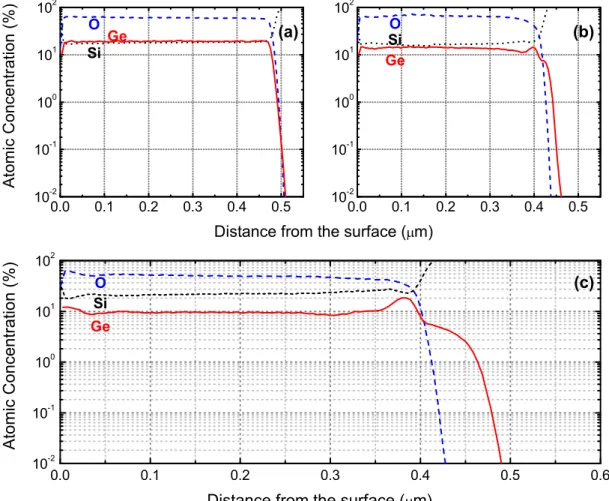
used for propagation loss measurements using prism coupling method along with (b) a simulated mode profile. . . 42 4.7 SIMS profiles for the (a) as deposited GeH4= 90 sccm , (b) GeH4=
90 sccm and annealed at 1000 , and (c) GeH4= 120 sccm and
4.8 (a) Scanning electron and (b) transmission electron microscopy im-ages of the Ge precipitate formed at the silicon/dielectric interface for the sample sims3. . . . 46 4.9 Coupled light spectrum for both (a) triangle and (b) trapezoid
shaped prisms for PS films. . . 50 4.10 Light coupling efficiency vs. loaded force for both TE and TM
polarizations as observed for PS films. . . 52 4.11 Typical spectrum of guided modes with TM (or TE) polarized light
for PMMA. . . 53 4.12 Calculated refractive index values vs. thickness change of PMMA
films. A small but steady increase of the refractive index is clearly observed for both polarizations. . . 54 4.13 Birefringence vs. thickness change of PMMA polymer films. . . . 55 4.14 Change of the TE and TM refractive index for PS films with change
in the film thickness. . . 59 4.15 Change of the TE and TM refractive index for BCB films with
change in the film thickness. . . 60 4.16 Change of birefringence for PS films with change in the film thickness. 61 4.17 Detailed representation of the system used for pressure application
and readout in the modified prism coupler setup. . . 62 4.18 Experimental data for variation of ∆y/y0 with the applied force
F for PMMA films with thicknesses of 3.10, 3.22, 4.30, 4.75, and 6.10 µm. Note that the coupling is completed for F > 15 N. . . . 64 4.19 Variation of the out–of–plane elastic modulus with films thickness
5.1 Thermal poling apparatus consisting of a hot plate and a pyrex beaker oven. The contact between the substrate and electrodes is maintained by a ceramic clamp. . . 83 5.2 Calibrated MF curves measured for (a) sample #2, (b) sample #3,
and (c) sample #4. . . 85 5.3 The recovered optical nonlinearity depth profiles of sample #2
(blue), #3 (red) and #4 (black). . . 86 5.4 Left axis (blue curve): the ratio of the χ(3) of the PECVD grown
germanosilicate layer to the χ(3) of fused silica; right axis (green
curve): maximum built-in E-field measured in poled germanosili-cate films. . . 87 5.5 Charge density of poled sample #4, inferred by differentiating the
recovered d33(z) profile. . . . 89
5.6 The recovered nonlinearity profiles of sample #1 (blue), #3 (red), #6 (black) and #7 (green). . . 90 5.7 The recovered optical nonlinearity depth profile of samples #3
(red) and #5 (blue). . . 92
6.1 Fundamental mode profiles for (a) TE and (b) TM polarization of germanosilicate ridge waveguide as calculated by BPM. . . 96 6.2 Index of refraction for the germanosilicate sample grown with
GeH4 flow rate of 50 sccm as a function of wavelength as
mea-sured by ellipsometry. . . 97 6.3 Schematic representation of the growth process of the layered
structure for germanosilicate optical waveguides. . . 99 6.4 Schematic representation of the process of waveguide strip
6.5 Formation of irregularities at the edges of the metal stripes af-ter the liftoff process, as viewed with optical microscope. These wriggles are potential scattering sources increasing the propagation losses in optical waveguides. . . 102 6.6 SEM images of the formed edge defects of Cr stripes in the
overde-veloped samples after liftoff process. The over deoverde-veloped PR struc-ture (a) and the formed edge defects (b) are clearly identified. . . 103 6.7 Index of refraction for the PECVD as-grown SiOx film as a
func-tion of wavelength. . . 104 6.8 The final structure of the waveguide as viewed through an optical
microscope. The Si, SiO2, SiOx, and ITO layers are clearly
identi-fied, while it is difficult to distinguish the SiOx:Ge layer sue to the
similar material nature. . . 105 6.9 Optical waveguide devices measurement setup. . . 107 6.10 Insertion loss results for the TE and TM input polarized light for
identical waveguides of different length. The waveguide geometry is depicted in the inset. . . 108 6.11 Insertion loss results for the TE and TM input polarized light
for identical waveguides of different length and lower and upper cladding thicknesses increased to ∼4 µm. The waveguide geometry is depicted in the inset of the figure. . . 109 6.12 A schematic picture of a single bus microring resonator channel
dropping filter. . . 111 6.13 Calculated transmission characteristics of a sample single bus
mi-croring resonator. . . 113 6.14 Schematic representation of the effective index model used to
6.15 Waveguide layout model used for BPM simulation of bending losses in curved structures. . . 117 6.16 Bending loss results as extrapolated to 90° as a function of arc
radius as calculated both analytically and by 3D-BPM. . . 118 6.17 (a) Waveguide layout model used for 3D-BPM calculation of
cou-pling coefficients, κ. (b) A sample simulation output for a device with a gap of 1 µm and R=1000 µm. . . 119 6.18 Coupling factors as calculated by 3D-BPM simulations as a
func-tion of gap length for various radii. . . 120 6.19 A two-step and two-chip photolithographic mask layout as
de-signed with MEMS L-Edit and used for fabrication of germanosil-icate ring resonator devices. . . 122 6.20 An optical microscope image of a 750 µm radius ring resonator.
The inset shows in detail the coupling region and the 0.8 µm gap between the bus and ring waveguides, the widths of the waveguides are 3.0 µm. . . 124 6.21 A schematic picture of the ring resonator device with the top ITO
electrode structure. The insets show the optical micrographs of the top ITO electrode layers placed onto the waveguide ridge structures.125 6.22 Transmission spectra results for some of the ring resonator devices
with different radii as a function of wavelength at TE polarization. 126 6.23 Transmission spectra results and analytical function fit to a single
bus microring resonator with R=1000 µm and gap=1.3 µm at TE polarization. . . 128
6.24 Optical microscope image of the coupling region between the bus waveguide and the ring structure in a resonator device with R=1000 µm and gap=1.3 µm. The left inset of the figure shows the magnified portion of the coupling region. The discontinuity region (trench) formed during the PECVD growth of the upper silicon oxide cladding layer is highlighted in the insets and is marked with ¬. . . 131 6.25 Transmission spectra result for a microring resonator with R=1000
µm and gap=1.3 µm at both TE and TM polarizations fabricated
without the upper and lower ITO layers. . . 132 6.26 The measured (a) Q-factors, (b) Finesse values, and (c) the
calcu-lated propagation loss values determined from the function fitting for the ring resonator devices fabricated with and without ITO layers. The lines are drawn to guide the eye. . . 133
2.1 Growth parameters for silicon oxide, nitride, and oxynitride layers. 11 2.2 Refractive index values for some of the silicon based dielectrics. . 14
3.1 Growth parameters for germanosilicate films used in FTIR mea-surements. . . 23 3.2 N−H bond str. concentration calculation details for
germanosili-cate films by using FTIR transmittance spectroscopy. . . 28
4.1 Summary of the measurements of index of refraction for ger-manosilicate layers for TE & TM polarization at λ = 633 and 1550 nm, with varying GeH4 flow rate. . . 40
4.2 Propagation loss variation with GeH4 flow rate for three
represen-tative germanosilicate planar waveguides at λ = 1.55 µm. . . . 43 4.3 List of the germanosilicate samples investigated by secondary ion
mass spectroscopy. . . 44 4.4 Summary of all refractive index and thickness measurements for
polymer films in this study. . . 55
4.5 Results of FEM analysis and elasto-optic coefficient calculations. The tabulated data includes the initial thickness of the guiding polymer films (y0), maximum film thickness change with the
ap-plied pressure (∆ymax), calculated elastic moduli of the layers (E),
constants (K1, K2, and K3) as determined by FEM simulations, the
slope values (mxand my), and the calculated elasto-optic constants
C1, C2 and C. . . 69
5.1 Characteristics and poling time of germanosilicate films poled in air at ∼5 kV and ∼280. . . 82
6.1 Optimized process parameters used in reactive ion etching of ger-manosilicate layers. . . 104 6.2 Summary of the propagation loss values for germanosilicate
waveguides with different thicknesses of the cladding layers. . . 110 6.3 The geometrical structures of the devices included in the
pho-tolithographic mask. Five different radii with several gap lengths for each were included, resulting in a total of 16 devices to be placed on two separate chips. . . 121 6.4 Summary of the measured characteristics of some of the
ger-manosilicate microring resonators. . . 127 6.5 List of some of the critical parameters for germanosilicate ring
resonators. The simulated values correspond to the expected pa-rameters based on calculations and the experimental values are extracted from the fit of the analytical function of Eq. (6.20) to the measured transmission spectrum of each device. . . 129
Introduction
Since the discovery of fire, light and optics have0 been employed in communicating information. It has been used to exchange information both on the sea and on the ground. Today, information affects every aspect of our lives because of the enormous improvements in the computer and communication technologies [1]. Everyone would agree that our lives would be totally different without computers, cell-phones, internet, satellites, and many other information processing tools. Today, the increasing importance of information access and manipulation, forces us to process it faster, with fewer inaccuracies, at a lower cost, and with a system which consumes less space.
1.1
Milestones in the Field of Photonics
Close connection between physics and communications started after 1876 with the invention of telephone by A.G. Bell. The field of electromagnetism became an important topic at those times. It is an interesting fact that only five years after the invention of the phone, it underwent a rapid commercialization [1]. A similar breakthrough had become possible only after 1960’s when T. Maiman demon-strated the first pulsed ruby laser. Providing the coherent light source was one of the major impacts of physics. It stimulated the research in fiber optics resulting
in first low loss (20 dB/km) optical fibers developed in 1970’s by F. P. Kapron
et al. These fibers were designed to operate at 850 nm, the GaAs/AlxGa1−xAs
laser wavelength. The development of lasers on InP/InGaAsP materials system operating at wavelengths of 1300 and 1550 nm made it possible to shift the com-munications wavelengths to this low-loss region. Silica fibers, as a result, were developed to reach losses as low as 0.15 dB/km by 1985, making it possible to establish the first long haul transatlantic optical fiber system that was installed in 1988 [1]. Since then, the capacity of the commercial fibers has increased in accordance with the Moore’s law [2] for integrated circuits, i.e. doubling each year.
The next stage in the field of communications and photonics can be identified as the trend of evolving towards planar waveguides instead of relying completely on optical fibers. Although optical fiber components can perform many of the passive optical functions, the notion of planar integration is becoming more and more important. It offers potential technological and economic advantages. The compactness it provides makes reduction of many critical devices down to single chip dimensions possible. Moreover, integrating complex functions into chips, that are made processing a single wafer, reduces the cost abruptly [3]. Above all, the available integrated circuit processing technologies facilitate the use of silicon based materials in the area of integrated optics.
1.2
Why Silicon Based Dielectrics?
Silicon technology was and remains as the most dominant force in electronic integrated circuits and it seems that this will continue in the near future [2, 4]. Si-based technologies offer crucial advantages in terms of both performance and cost, which makes it more attractive over all other competing technologies. The major drawback of this technology has been lack of a light source (Si being an indirect bandgap material), however, recently researchers have demonstrated a continuous-wave Raman silicon laser [5], which has made the technology even more promising.
The work towards implementation of silicon technology in the integrated op-tics area started ever since the notion of integrated opop-tics was introduced. There are several key factors for this application to be successful. First of all, any candi-date technology must provide waveguide structures with low propagation losses. Moreover, it should be compatible with microelectronics device processing and provide high reproducibility with reasonably low cost. The coupling between the optical integrated circuit devices and other elements such as optical fibers, light sources, and photodetectors is another important issue of consideration. Most of the materials used in integrated optics so far are classified as either low in-dex contrast (e.g. silica, LiNbO3, polymers) or high index contrast (e.g. InP,
SOI) [6]. The satisfaction of all of the above mentioned requirements simultane-ously for both of these systems is a challenging issue. In the low contrast systems the fiber-to-chip coupling efficiency is excellent due to the large size of the single mode waveguides, but they have low integration density since large bend radii (10-30 mm) are required for low loss operation. On the other hand, high contrast systems allow very small bending radii (below 0.5 mm) with low losses, how-ever efficient fiber-to-chip coupling is difficult to obtain due to small waveguide dimensions [7, 8].
In recent years, growing attention has been paid to silicon based dielectrics, such as silicon oxynitrides, silicon nitrides, and semiconductor doped silicon ox-ides, all combined with the name silica on silicon technology (SOS) [9–11]. This attention has been motivated mainly by their excellent optical properties such as well controlled refractive index and high transparency over a wide range (see Fig. 1.1) [3]. Silicon based dielectrics combine the properties of SiO2 together with
good chemical inertness and low permeability of high-refractive-index materials, e.g. Si3N4, germania, etc. Furthermore, the index of refraction of these layers can
be easily adjusted continuously over a wide range between 1.45 (SiO2) – ∼2.0.
This is a very attractive property as it allows for fabrication of waveguides with desired characteristics of fiber match and compactness [10, 11]. Moreover, the growth of silicon based layers is done by well established standard silicon inte-grated circuit processing technology, which is also a key point towards low cost mass production.
Rayleigh Scattering Impurity Absorption (e.g. O-H, N-H) Infrared Absorption Wavelength ( m)m Attenuation (dB/km)
Figure 1.1: Attenuation characteristics of a typical silica fiber guide. (Adapted from [12]).
The major drawback of this technology originates from the relatively high propagation losses introduced by the impurities during the growth of the material [13]. In particular, loss at λ=1.55 µm is known to be caused mainly by N−H and O−H bonds incorporated into the film matrix (see Fig 1.1). The reported values for propagation losses are larger than 2 dB/cm at λ=1.55 µm, although this has not been analyzed systematically [14]. To reduce these loss values, it is common practice to anneal the as-grown layers at temperatures as high as 1100 for prolonged times [13, 15, 16]. It would be of great interest to obtain silicon based dielectric layers with reasonably low propagation losses in as-deposited form, avoiding the need for the annealing process.
The silicon based dielectrics are deposited using various techniques. The most commonly used growth technologies are plasma enhanced chemical vapor de-position (PECVD) and low pressure chemical vapor dede-position (LPCVD). The PECVD process is found to be more efficient in controlled deposition of films with refractive indices below 1.7 [6]. The deposited layers have good uniformity of the refractive index and layer thickness with run-to-run reproducibility. The waveguides fabricated by this technology have the following structure: silicon is used as a substrate and SiO2buffer layer is thermally grown on it to act as a lower cladding layer for the silicon based dielectric core film on top of which SiOx is
deposited to provide symmetric structure [17]. The reported propagation losses of the waveguides vary between 1.5-10 dB/cm (λ = 1.55 µm) for as deposited films and are reduced to 0.2-0.36 dB/cm for thermally annealed films [6,7,18–20]. The application area of any material system includes variety of integrated optical devices. Among these, microring resonators attract special interest. Re-cently a lot of research has been carried out for use of microring resonators in integrated optics as all-optical switches, add-drop filters, electro-optic modula-tors, etc [21–23]. Optical Ring Resonators (RRs) offer useful components for wavelength filtering, multiplexing, switching, and modulation. The key perfor-mance characteristics of the RRs includes Free-Spectral Range (FSR), finesse, quality factor, resonance transmission, and extinction ratio. These quantities de-pend not only on the device design but also on the fabrication tolerance. Current challenges in the field are to produce dielectric microring resonators with low-loss, large free-spectral range and of desired characteristics of resonant wavelength ad-justment and filter linewidth [24]. Application of silicon based dielectrics on such devices has recently been studied in detail [25,26] motivated by the fact that these materials are relatively inexpensive and their index contrast is easily adjustable. Moreover, their dimensions are two or three times larger than their semiconduc-tor counterparts, which allows efficient usage of optical lithography without the need for e-beam lithography. Silicon based dielectrics, therefore, offer a promising platform for applications of ring resonator devices [27].
1.3
Contribution of This Work and
Organiza-tion of the DissertaOrganiza-tion
In accordance with the main goal of this work, that relies on the utilization of silicon based dielectrics and their optimization for applications in integrated optics, an emphasis was given to the compositional and optical properties of these materials.
investigated the compositional properties of silicon oxide, silicon nitride, silicon oxynitride, germania, and germanosilicate glasses and identified the germanosili-cate dielectrics as the most promising candidates for use in integrated optics.
In Chapter 3 we focused on detailed quantitative compositional analysis of the germanosilicate films using Fourier transform infrared spectroscopy. Compo-sitional analysis using FTIR spectroscopy showed that the amount of N−H and O−H related bonds exhibited a drastic decrease with increasing GeH4 flow rate.
In Chapter 4 we report on a first systematic study of propagation losses for different-index planar waveguides. This study had striking results in which pla-nar waveguides fabricated with germanosilicate core layers showed the lowest propagation loss values reported so far both for as deposited and annealed ger-manosilicate films at λ=1.55 µm, eliminating the need for costly and cumbersome annealing process. With a further step of improvement of the prism coupling technique, a new approach is proposed for elasto-optic characterization of thin polymer films. This completely new method allows us to determine and to cor-relate the optical anisotropy and out-of-plane mechanical properties in order to obtain the elasto-optical properties of thin polymer films, for the first time.
The investigations of optical properties of germanosilicate films continued with a focus on their nonlinear properties as described in Chapter 5. Of interest as potential electro-optic devices, we have concentrated on thermally poled low-loss germanosilicate films deposited on fused-silica substrates by PECVD. After opti-mizing the germane flow rate during deposition, the film thickness, and the poling time for maximum peak nonlinearity, we demonstrated a record peak nonlinear coefficient of ∼1.6 pm/V, approximately twice as large as the highest reliable value reported in a thermally poled fused silica glass.
Having optimized the compositional and nonlinear properties of germanosil-icate dielectrics, in Chapter 6 we have demonstrated several applications of this technology in the field of integrated optics. Since optical waveguides constitute the building blocks of many integrated optical devices, we had first concentrated on design and optimization of waveguides employing germanosilicates as the core
layers. The final step of our work was to design and implement microring res-onator devices based on germanosilicate layers with optimized finesse and quality factors.
Finally, in Chapter 7 we conclude with a summary and discussion of the key results of this PhD work.
Silicon Based Dielectrics –
General Overview
In this chapter, the results on compositional and refractive index characterization obtained on silicon based dielectrics grown by Plasma Enhanced Chemical Vapor Deposition (PECVD) technique are summarized. After a brief description of the PECVD method, results for silicon oxide and silicon oxynitride films are presented, and then an analysis of the effects of adding germanium to these layers are reported.
2.1
Plasma Enhanced Chemical Vapor
Deposi-tion
The field of microelectronics has been using chemical vapor deposition (CVD) techniques for several decades for deposition of various dielectrics primarily aim-ing applications such as insulation, maskaim-ing, optical guidaim-ing, etc. This technique can be defined as a process where thin solid films are grown as a result of chem-ical reactions of the precursor gases. The PECVD technique in particular, has
APC Rough Pump Vent SiH4 NH3 N O2 GeH4 Temperature Controller RF Plasma
Figure 2.1: PECVD reactor structure.
received wide application in the area of integrated optics. The major advan-tage of plasma enhanced (or plasma–assisted) CVD comes from its capability of growing films at relatively low temperatures (150–350 ) [28]. In conventional CVD processes, the standard temperature of operation is in the range of 700–900 , which limits its applicability to device fabrication in which metallization and other temperature sensitive preocesses are involved. The operation at such low temperatures for PECVD technique is possible due to the addition of electrical energy to the environment in the form of RF power, resulting in glow discharges. The system used in our studies is a parallel-plate type Plasmalab 8510C reac-tor (see Figure 2.1). The radio frequency (RF) generated glow discharge (plasma) takes place between two electrodes which are separated by 2 cm. The plates are 24 cm in diameter and the RF power that establishes the plasma is applied to the upper electrode while the samples are placed on the bottom grounded electrode that can be heated up to 400. The system can be operated at a pressure range of 0.1–10 Torr. Applied RF frequency is 13.56 MHz with a maximum power of
300 Watts. The available gases that can be used as precursors for film growth are silane (2% SiH4/N2), ammonia (NH3), and nitrous oxide (N2O). A germane
(2% GeH4/He) gas line has later been introduced in order to be able to dope
the grown films with Ge. The structure of the films grown by this technique is amorphous in nature and their compositional characteristics are to be discussed extensively in the following chapters.
2.2
Silicon Oxide and Oxynitride Layers
The major problem for integrated optics applications in the PECVD grown silicon based layers has been reported to be the incorporation of hydrogen and nitrogen in the form of N–H bonds into the film matrix [7, 29]. Although there have been a considerable number of both compositional and device related studies on these films separately, there has been a lack of systematic analysis comprising all three silicon based layers [30, 31], i.e. silicon oxides, nitrides, and oxynitrides. Namely, the dependence of the optical properties on film composition and growth para-meters needs to be established for the whole range of compositions starting from silicon oxide and ending with silicon nitride films. During our M.Sc. study, an attempt was made to establish such a relation, to identify possible drawbacks of the films in the above mentioned range and to possibly eliminate them in a sys-tematic way, for the first time [13]. Their deposition, material characterization, and treatment towards loss minimization, and finally the fabrication and char-acterization of single-mode waveguides were analyzed. A brief summary of the results of our M.Sc. study is included in this section for the sake of completeness. The stoichiometry of the PECVD grown layers typically deviates from their “ideal” counterparts. Namely, instead of SiO2 one obtains SiOx due to small
amounts of hydrogen and nitrogen incorporated into the film, resulting in a re-fractive index larger than 1.46. For convenience, they will be denoted as SiNx
and SiON, respectively.
Table 2.1: Growth parameters for silicon oxide, nitride, and oxynitride layers. Silane (2% SiH4/N2) Flow Rate 180 sccm
N2O Flow Rate 25–450 sccm
NH3 Flow Rate 0, 15, 30 sccm
Process Pressure 1000 mT orr
RF Power 10 W
Temperature 250 , 350
at 180 sccm, while that of ammonia was either 0, 15 or 30 sccm, and the flow rate of nitrous oxide was varied between 0 and 300 sccm (see Table 2.1 for details). The index of refraction and thickness of the grown films were measured by an automated Rudolph Research/AutoEl III ellipsometer at a wavelength of 632.8
nm. Typical accuracy values of the measurements were ± 0.01 and ± 20 ˚A for the index of refraction and thickness of the films, respectively. In addition, the thickness values of some of the layers were measured by Sloan Dektak 3030ST stylus profilometer.
As seen from Fig. 2.2, the values of the refractive index of both silicon oxide films grown at 250 and 350, decrease from a value of about 1.56 down to 1.47 with increasing N2O flow rate. At N2O flow rates higher than 150 sccm the
decrease in the refractive index saturates. The high index region in Fig. 2.2 is due to silicon rich films. As the N2O flow increases, a large amount of oxygen and
some nitrogen is incorporated into the films, resulting in refractive index closer to that of stoichiometric SiO2. The silicon oxide characterizations were performed
at two different growth temperatures of 250 and 350 in order to compare the qualities of the films grown. It was observed that the growth rate decreases slowly as the substrate temperature is increased. For N2O flow of 25 sccm, the
growth rate at 250 is 340 ˚A/min, whereas at 350 it decreases down to 290 ˚
A/min. This can be regarded as an indication that the films grown at higher temperatures are denser and contain less microvoids, which was also verified by monitoring the wet chemical etch rates of these layers. It is well known that etch rates obtained with wet chemical etch (e.g. HF) are smaller for denser SiOx
films. Therefore, the temperature of 350 was chosen for the growth of silicon nitride and silicon oxynitride films in order to obtain films suitable for optical
0 75 150 225 300 375 450 1.44 1.47 1.50 1.53 1.56 1.59 1.62 1.65 1.68 SiON (NH 3 =30 sccm) SiON (NH 3 =15 sccm) SiO x (350 o C) SiO x (250 o C) I n d e x o f R e f r a ct i o n N 2 O Flow Rate (sccm)
Figure 2.2: Variation of index of refraction of SiOx and SiON films with N2O and NH3 precursor gases flow rates and growth temperature.
applications. Moreover, the hydrogen incorporation into the layers is reported to be less at higher deposition temperatures [28], thus resulting in potentially low propagation loss waveguide materials.
A general trend of decreasing refractive index with increasing N2O ratio was observed in all cases (see Fig. 2.2) (for both silicon oxide and oxynitride layers), which comes about because of oxygen’s greater chemical reactivity compared to nitrogen. In addition, as the flow rate of ammonia was increased, the film index increased due to their higher nitrogen content, thus gaining more resemblance with the silicon nitride layers. It was found that increasing the nitrous oxide flow rate results in an increase of film growth rate as well. Moreover, the deposition rate was observed to be decreasing with increasing ammonia flow rate. The decrease of the growth rate with increase in nitrogen concentration in the film
can be explained by increasing probability of the nitrogen related bonding so that the nitrogen concentration in the film increases [32]. Thus, the layers become more silicon nitride–like, the growth rate of which is smaller than that of silicon oxides [13]. In fact, if we consider the growth rates for these films, they increase in the following order: silicon nitride, silicon oxynitride, silicon oxide, exhibiting a smooth transition of the physical properties of silicon oxynitride from those of silicon oxide to silicon nitride [13, 33].
The compositional properties of these three types of films were investigated via Fourier transform infrared transmission spectroscopy (FTIR). Special attention was given to the absorption band of N−H bond stretching vibration, since its first overtone is known to be the main cause of the optical absorption at 1.55 µm wavelength (the technique is to be discussed in detail in the following chapters) [7, 29]. For silicon oxide films the N−H bond concentration was found to vary between 7.4 × 1021 cm−3 and 0.4 × 1021 cm−3, while the same bond variation
for silicon nitride layers was between 9.6 × 1022 cm−3 and 7.9 × 1022 cm−3.
For the silicon oxynitride films, the corresponding variation of the N−H bond concentration was observed to be 0.6–1.7 × 1022 cm−3. It was found that the
observed N−H bonds resulted in propagation losses larger than 4 dB/cm. Low-loss waveguides (<1 dB/cm), therefore, were only possible to obtain after an annealing treatment at temperatures higher than 1100 [13].
2.3
Germanium Doped Layers
During the first stage of this Ph.D work, there were three different precursor gases available for film growth, namely silane, nitrous oxide, and ammonia. Tuning the refractive index of the “optical–grade” layers was possible only through variation of the N2O gas flow rate at fixed flow of SiH4 and NH3. However, during the
M.Sc. study [33], it was verified that this gas acts as a primary source for the N−H bonding in the layers, which needs to be eliminated in order to decrease the propagation losses in the waveguides [13]. In order to be able to vary the refractive index of the PECVD grown material without possibly including extra
Table 2.2: Refractive index values for some of the silicon based dielectrics. Film PECVD Gas Flow Rates (sccm) Refractive Index
Type SiH4 GeH4 N2O NH3 (λ = 632.8 nm)
SiOx 180 - 225 - 1.46 SiON 180 - 100 15 1.54 SiON 180 - 225 15 1.50 SiON:Ge 180 50 225 15 1.76 SiOx:Ge 180 20 225 - 1.49 SiOx:Ge 180 50 225 - 1.53 SiOx:Ge 180 90 225 - 1.66 SiOx:Ge 180 120 225 - 1.94
N−H bonds into the films, we have introduced germane (2% GeH4/He) gas into
the PECVD system. This gas has given us an opportunity to dope the films with
Ge.
As far as integrated optical applications are concerned, using germane as the core dopant and silica as the cladding, ensures nearly identical characteristics for planar waveguides with the existing fiber technology [15]. Moreover, promising phenomena such as significant UV photosensitivity [34] and second–harmonic generation [35] have already been shown in germanosilicate waveguides, providing great potential for optical applications [36].
As a result, in addition to silicon oxide, silicon nitride and oxynitride films, we gained a capability of growing the following types of dielectric films: germanosil-icate (SiOx:Ge:N:H ), germane doped silicon oxynitride (SiON:H:Ge), and
ger-manate (GeOx:N:H ) glasses. Table 2.2 gives examples for some of the refractive
index values obtained by combination of different flow rates of the available gases (as measured by ellipsometry at λ = 632.8 nm).
In addition to the index of refraction, we focus on the compositional prop-erties of the grown layers and mainly aim for low N−H bond concentration in the films with possibly high refractive index. In light of these criteria, various di-electrics (germanosilicates, germanium doped oxynitrides, and germanate glasses) were investigated. An important initial finding was that the germanate and high– germanium–content glasses are easily oxidized shortly after the deposition. FTIR
4200 4000 3800 3600 3400 3200 3000 2800 A b s o r b a n c e ( a . u . ) W avenumber (cm -1 ) 20sccm 35sccm 50sccm 75sccm 90sccm 105sccm 120sccm 130sccm germanate O H N H
Figure 2.3: Comparison of the O−H and N−H stretching bands as obtained with FTIR absorbance spectroscopy for germanosilicate and germanate films as a function of GeH4 flow rate at fixed SiH4 and N2O flows.
analysis shows large amounts of O−H bonds indicating the possible absorption of water vapor. This property ruled out the possibility of their usage as a dielec-tric material for integrated optical devices. FTIR spectroscopy also shows that the most suitable material, compared to the previously mentioned ones due to their minimum N−H bond content (comparing materials with the same index of refraction) turned out to be the germanium–doped silica (or germanosilicate
SiOx:Ge) films. Germanate (GeOx) glasses contained the largest amount of the
N−H and O−H (see Fig. 2.3), which decreased in silicon oxynitride layers and were minimum in germanosilicate glasses. Figure 2.3 shows the variation of the O−H and N−H stretching bands with the GeH4 flow rate for germanosilicate
films. The quantitative analysis of these bonds in germanosilicate films will be a subject of another chapter. At this point, the most important finding was that the films suitable for integrated optics are germanosilicates, rather than silicon oxynitride and Ge doped oxynitride films, due to their low N−H bond content
0 20 40 60 80 100 120 1.2 1.4 1.6 1.8 2.0 2.2 GeH 4 Flow Rate (sccm) I n d e x o f R e f r a ct i o n
Figure 2.4: Variation of index of refraction for germanosilicate layers with GeH4
flow rate.
and hence low propagation losses.
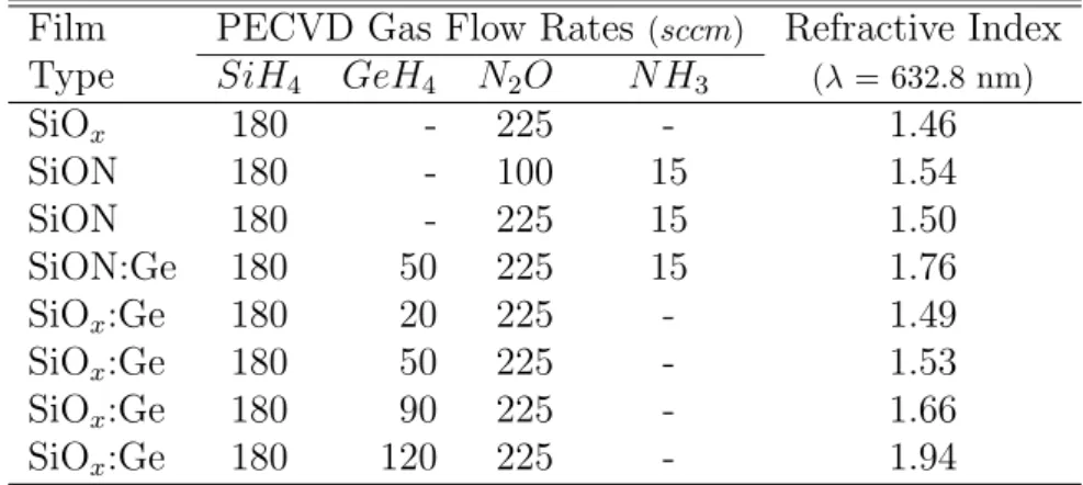
The effect of adding Ge into SiOx layers on refractive index of the material is
of great interest. Therefore, the variation of index of refraction with GeH4 flow
rate was characterized (see Fig. 2.4). The samples analyzed were grown at 350 , with 10 W RF power, under 1 Torr pressure, and using constant 180 sccm SiH4 and 225 sccm N2O flow rates. The GeH4 flow was varied between 0 and
120 sccm resulting in a steady refractive index increase from 1.46 up to 1.94, as measured by an ellipsometer (λ = 632.8 nm). The index of refraction was lower at low GeH4 flow rates and increased with increasing Ge incorporation into the
film. The observed growth rates, however, did not show a significant change with the change of germane flow. A small decrease from about ∼340 ˚A/min down to
∼290 ˚A/min was identified.
on germanosilicate glasses. These dielectric layers will further be investigated in terms of suitability for integrated optical applications. One of the methods to be used for the characterization of these layers will be the prism coupling technique. This method is to be discussed in detail In Chapter 4.
Germanosilicate Dielectrics I:
Compositional Analysis Using
FTIR
Based on analysis of Section 2.3, germanosilicate is selected to be the material system on which further investigations are to be carried out. Considering the goals of our work, in addition to characterizing the optical properties of germanosilicate films, we would benefit much from learning about the composition of grown layers. Thereby, an attempt is made towards relating the material composition to film characteristics such as index of refraction and optical loss. For this purpose, widely-used Fourier Transform Infrared (FTIR) spectroscopy together with prism coupling methods (PCM) will be employed. Below, some general remarks on infrared spectroscopy are given, followed by the description of the experimental setup. Subsequently, the results obtained from a thorough compositional analysis are presented.
3.1
General Remarks on FTIR Spectroscopy
Infrared (IR) absorption makes use of the vibration of atoms in molecules. The spectrum is obtained by having IR radiation pass through a sample and analyzing the absorption features at particular energies, which in turn correspond to the frequency of vibration of a part of a molecule in the structure [37].A polyatomic molecule consisting of N atoms has 3N −6 (3N −5 if it is linear)
normal modes of vibration [38]. Actually, the total vibrational motion of the
molecule is resolved into components which consist of mixture of angle–bending and bond–stretching vibrations called as the normal modes (see Figure 3.1). In a normal mode of vibration, all the nuclei move in phase, have the same frequency of vibration, and in general move with different amplitudes. In this motion, the center of mass of the molecule does not move and the molecule as a whole does not rotate. Moreover, any vibrational motion of this polyatomic molecule is expressible in terms of linear combination of its normal modes. Here it should be mentioned that, in addition to the basic stretching and bending vibrations, there are other termed kinds such as rock, twist, scissors, wag, and breathing, which are frequently used to describe the group vibrations of molecules [33].
As an illustrating example one can look at the possible transitions in a vi-brational spectrum that are possible for diatomic molecules. In the framework of quantum mechanics, this is determined by the interaction of the dipole moment
(a) (b) (c)
Figure 3.1: Illustration of (a) bending, (b) symmetric stretching, and (c) anti-symmetric stretching vibrations for a polyatomic molecule.
of the molecule with the electric field component of the incident radiation [38]. Explicitly, the transition probability is given by the square of the transition dipole moment ~Rnm, given by ~ Rnm = Z Ψ∗ nµΨˆ mdτ, (3.1)
where ˆµ is the electric dipole moment operator and
ˆ
µ =X
i
qi~ri, (3.2)
where the sum is carried over all nuclei and electrons of the molecule, qi is the
charge and ~ri is their position vector. The transition dipole moment ~Rnm can be
thought as the oscillating electric dipole moment due to the transition.
For a diatomic molecule of two different species the electric dipole moment µ is non–zero and varies with distance, x. This variation is expressed as a Taylor series expansion about equilibrium point xe, referring to equilibrium internuclear
distance, as ~µ = ~µe+ µ dµ dx ¶ xe (x − xe) + 1 2! µ d2µ dx2 ¶ xe (x − xe)2+ .... (3.3)
Now, for a molecule in a given electronic state, the transition dipole moment takes the form of
~ Rv0 v00 = ~µe Z Ψ∗ v00Ψv0dx + µ d~µ dx ¶ xe Z Ψ∗ v00(x − xe)Ψv0dx + .... (3.4)
The first term of this equation is zero because the vibrational wave functions for different v (states) are orthogonal. The second term is non–zero if
∆v = ±1, (3.5)
which imposes a vibrational selection rule. Another condition for the non– vanishing of this term is that the dipole moment should be a function of the internuclear distance x. This means that homonuclear diatomic molecules, e.g.
N2 and H2, have zero dipole moments for all bond lengths and, therefore, show
no vibrational spectra. For the higher terms of Eq. (3.4) we would expect that their contribution is small and can thus be neglected. If they are neglected, the harmonic oscillator model would give us only single vibrational absorption at a
specific frequency; otherwise, the higher terms do give rise to overtone
transi-tions of ∆v = ±2, ±3, ... (i.e. v0 → v2, v0 → v3, etc.) with rapidly decreasing
intensities.
The final remark is about the selection rules for infrared active vibrations. The main rule is that any normal mode will have a vibrational spectrum only if its displacements cause a change in the dipole moment. The process of this deter-mination of the vibrational modes that are infrared active is performed by making use of group theory, i.e., identifying the symmetry properties of the molecule and possible vibrations that result in dipole moment change.
3.2
Experimental Setup
Throughout our experiments a Bomem H&B Series FTIR spectrometer has been used (see Fig. 3.2). Its basic operation relies on a Michelson interferometer, which is built into the spectrometer. The advantages of this technique over the other spectroscopic methods derive from using a large aperture at the signal input and having the entire spectrum at once at the output. Namely, using a large aperture results in a large energy throughput and is called the Jacquinot advantage. Moreover, the ability to simultaneously process the entire spectral range in a single scan gives an advantage known as the Fellget advantage [33].
As a source in the spectrometer, a Nerst solid glower is used, which radi-ates continuous light in the mid–infrared region in accordance with blackbody radiation. The light is then directed to the beam splitter of the Michelson inter-ferometer, after which it is reflected from two perpendicular plane mirrors one of which is movable. The radiation reaching the detector (pyroelectric deuterium tryglycine sulfate: DTGS ) consists of two components that have a path difference of δ with its magnitude changed by displacing the movable mirror. The intensity of light measured at the detector, which represents the interference between the two beams, is of the form of
I(δ) =
Z ∞
0
Michelson Interferometer: Mobile mirror Beam splitter Fixed mirror Sample Interferogram Spectrum Fourier-Transform
Figure 3.2: The FTIR experimental setup used for infrared absorbance measure-ments.
where ω is the wavenumber and B(ω) is the source intensity at that wavenumber. This expression is also called as interferogram and its Fourier transform gives the desired spectrogram of the transmitted intensity as a function of the wavenumber, i.e. B(ω) given by
B(ω) = 2
Z ∞
0
I (δ) cos(2πωδ)dδ. (3.7)
The process of this transformation is performed by a computer.
In order to understand the significance of the spectrum, it is necessary to closely look into what it represents. When we pass radiation of intensity I0
through a sample, the transmitted intensity is I. The ratio I/I0 is called the
transmittance of the sample. If we have a sample of thickness t and concentra-tion c of bonds that absorb light, we can define absorbance A, which is directly proportional to above quantities as
A = αtc, (3.8)
where α is a constant of proportionality called as molar absorptivity having dimen-sions of inverse concentration × length. The absorbance (A) and transmittance
(T ) are related by A = log10 µ I0 I ¶ = log10 µ 1 T ¶ , (3.9)
which is known as Beer’s law. In the obtained IR spectrum the total intensity of a specific absorption band is measured by the integrated intensity, which is carried out over the band of interest. The integrated absorption coefficient is defined by
(see e.g. [39]) Z
band
α(ω)dω. (3.10)
The results of Eqs. (3.6)–(3.10) are to be used in the following sections for determination of the relevant bond concentrations.
3.3
IR Analysis of Germanosilicate Layers
A series of germanosilicate films was grown by using parallel–plate type Plasmalab
8510C PECVD reactor. The layers were grown on high resistivity silicon wafers
with polished sides at 350 , under a pressure of 1 torr, and with an RF power of 10 W at a frequency of 13.56 MHz, applied to the plates with a diameter of 24
cm (see Table 3.1 for summary). Silane (2% SiH4/N2) and nitrous oxide (N2O)
gas flow rates were kept constant at 180 and 225 sccm, respectively, while that of germane (2% GeH4/He) was varied between 0 and 70 sccm.
The compositional analysis of the germanosilicate films were performed by making use of Bomem H&B Series FTIR spectrometer. The spectra were obtained
Table 3.1: Growth parameters for germanosilicate films used in FTIR measure-ments.
Silane (2% SiH4/N2) Flow Rate 180 sccm
N2O Flow Rate 225 sccm
Germane (2% GeH4/He) Flow Rate 0–70 sccm
Process Pressure 1000 mTorr
RF Power 10 W
250 500 750 1000 1250 1500 A b so r b a n ce ( a . u . ) W avenumber (cm -1 ) S0 S1 S2 S3 S4 S5 S6 S7 Si O r ock G e O bend Si O bend G e H bend G e O str . Si O s.str . Si O as.str .
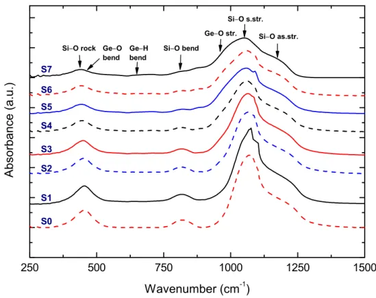
Figure 3.3: Infrared absorption spectra of germanosilicate samples at 250–1550 cm−1 range with the the following GeH
4 flow rates; s0: 0, s1: 5, s2: 10, s3: 20,
s4: 30, s5: 50, s6: 60 and s7: 70 sccm.
in the 5500–250 cm−1 range with 8 cm−1 resolution. The thicknesses of the
SiOx:Ge layers deposited for FTIR characterization were between 1.5 and 2.5
µm. Eight samples, s0−s7, with corresponding GeH4 flow rates of 0 (i.e. SiOx),
5, 10, 20, 30, 50, 60, and 70 sccm were used for compositional characterization. Thickness normalized absorbance spectra of the samples in 250–1500 cm−1 range
are shown in Fig. 3.3.
All the samples show a dominant absorption feature around 1050 cm−1 which
can be resolved into Si−O symmetric and asymmetric stretching and Ge−O stretching vibrations [40, 41] at frequencies of about 1065, 1150 and 980 cm−1,
respectively. Si−O rocking and bending vibrations were identified at ∼450 and
∼820 cm−1, while Ge−O and Ge−H bending vibrations were observed at ∼420
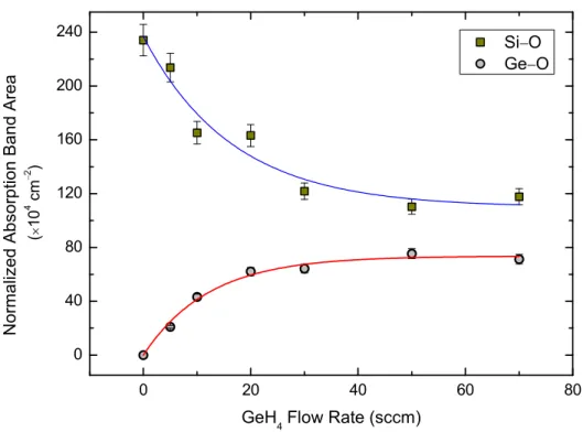
0 20 40 60 80 0 40 80 120 160 200 240 N o r m a l i ze d A b so r p t i o n B a n d A r e a ( 1 0 4 c m 2 ) GeH 4 Flow Rate (sccm) Si O Ge O
Figure 3.4: Variation of normalized absorption band area for Si−O and Ge−O related bonds with increasing GeH4 flow rate.
Analysis of the oxygen bond concentration was performed by integrating over the relevant bands. The bands were decomposed using nonlinear curve fitting, assuming that the peaks are in the form of symmetric Gaussians. The results of this analysis are plotted in Fig. 3.4. The normalized integrated absorption h R
bandα(ω)dω
i
of the Si−O bonds exhibited a gradual decrease, while that of Ge−O bonds showed a steady increase as a function of germane flow rate. Both reached saturation at a GeH4 flow rate of about 50 sccm. Assuming that the
infrared absorption cross section for the bonds of interest are similar, it can be stated that Si and Ge are incorporated into the film matrix at nearly equal concentrations for GeH4 flow rate of 50 sccm and larger, in the range investigated.
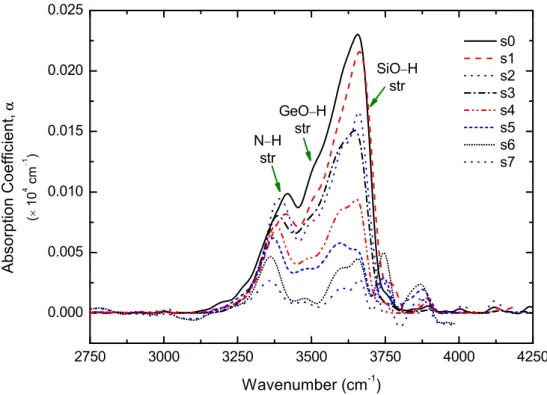
The most striking result of the FTIR analysis was that the observed amount of both N−H and O−H bonds decreased with increasing GeH4 flow rate (see Fig.
2750 3000 3250 3500 3750 4000 4250 0.000 0.005 0.010 0.015 0.020 0.025 A b so r p t i o n C o e f f i ci e n t , ( 1 0 4 c m 1 ) W avenumber (cm -1 ) s0 s1 s2 s3 s4 s5 s6 s7 N H str GeO H str SiO H str
Figure 3.5: FTIR absorption coefficient, α vs incident wavenumber for the ger-manosilicate samples in the N−H and O−H absorption band region.
stretching vibrations at ∼3470 and ∼3515 cm−1, and finally SiO−H stretching
vibrations at ∼3600 and ∼3665 cm−1 [43]. As the GeH
4 flow rate in the grown
samples increased, the N−H stretching vibrational frequency shifted about 30 cm−1 towards lower frequencies, while that of GeO−H and SiO−H remained
constant.
The vibration band of N−H bond stretching is of special interest for us, since it is the main cause of the optical absorption at 1.55 µm wavelength for the optical waveguides that we aim to fabricate. Thereby, special attention was paid to its properties and evolution for the studied samples. The N−H and O−H bond concentrations were calculated for all the grown layers by using the method of Lanford and Rand [39], by the expression
[X − H] = 1 2.303 σX−H × Z band α(ω) dω, (3.11)
where σX−H is the absorption cross section for the N−H or O−H bonds,
R
is the normalized absorption area of the band, and α = ³ 2.303 t ´ A is the absorption
coefficient, A being the absorbance and t the film thickness [32]. The integration is carried over the band of consideration, which was decomposed using nonlinear curve fitting and assuming that the peaks are in the form of symmetric Gaus-sians. The absorption cross section value σN −H = 5.3 × 10⁻¹⁸ cm2 used in our
calculations was obtained by Lanford & Rand [39] through a resonant nuclear reaction and the uncertainty of the calibration technique that they had proposed is reported to be about ±15% [44]. The corresponding value for O−H bonds was
σO−H = 1.5 × 10⁻²¹ cm2, obtained by Rostaing et al. [45]. In spite of the
rela-tively large uncertainty for the O−H bond absorption cross section, we believe that the results obtained can be safely used in the relative comparison of O−H bond concentrations of the samples. For other quantities such as peak wavenum-ber (ω), full width at half maximum (FWHM ), and normalized absorption band area (R αdω) of each absorption band we estimate typical uncertainty values of ±5 cm−1, ±5 cm−1, and ±4 %, respectively [13]. The results of the
calcula-tions of concentracalcula-tions are plotted in Fig. 3.6 and those for the N−H bonds are summarized in Table 3.2.
As seen from the figure, the N−H bond concentration has decreased from 0.43×1022 cm−3 down below our detection limit of 0.06×1022 cm−3, by a factor
of seven as the GeH4 flow rate increased from 0 (silicon oxide) to 70 sccm. As for
the O−H bonds, their concentration showed a sharp decrease, as well from about 2.27×1022cm−3 down to 0.23×1022 cm−3, by a factor of ten in the same germane
flow range. The observed decrease of these bonds has an important impact on propagation losses at λ = 1.55 µm of the waveguides grown using germanosilicate films. This issue is going to be further investigated by prism coupling technique and is to be discussed in the next chapter.
0 10 20 30 40 50 60 70 0.00 0.15 0.30 0.45 0 10 20 30 40 50 60 70 0.00 0.75 1.50 2.25 [ N -H ] ( 1 0 2 2 cm -3 ) (a) [ O -H ] ( 1 0 2 2 c m -3 ) GeH 4 Flow Rate (sccm) (b)
Figure 3.6: Variation of calculated N−H (a) and O−H (b) bond concentrations for germanosilicate samples with increasing GeH4 flow rate.
Table 3.2: N−H bond str. concentration calculation details for germanosilicate films by using FTIR transmittance spectroscopy.
GeH4 Flow Central Sum of Norm. N−H bond
Rate Frequency FWHM αmax Band Area Concentration
(sccm) (cm−1) (cm−1) (cm−1) (× 104cm−2) (× 1022 cm−3) 0(oxide) 3433 229 93 5.23 0.43 5 3416 176 80 3.44 0.28 10 3395 132 92 3.00 0.25 20 3392 145 78 2.79 0.23 30 3380 126 69 2.13 0.17 50 3370 139 61 2.07 0.16 60 3357 101 29 0.71 0.06 70 3353 124 25 0.75 0.06
Germanosilicate Dielectrics II:
Index of Refraction and
Propagation Loss Measurements
Using PCM
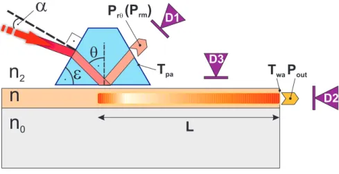
Optical characterization techniques are crucial for investigation of thin film prop-erties. Among various methods, prism coupling technique has received much interest due to several advantages it offers. Development of optical waveguide techniques has provided a convenient method for measuring the refractive indices and thicknesses of thin dielectric films. Due to the ease of operation and high measurement accuracy, the prism waveguide coupler has been used to determine the refractive index and birefringence of thin films as well [48–50, 52], making this method superior to standard ellipsometry. The prism waveguide coupler is particularly suitable for isotropic and anisotropic thin film studies because of the quantitative character of the information obtained.
In this chapter, the prism coupling method will be described in detail. After the prism coupling basics the description of the method for optical propagation loss measurements is presented. Next, the propagation loss characteristics of the germanosilicate films are investigated prior to a report on the effects of annealing of germanosilicate dielectrics. Finally, a study on the refractive index of the materials upon application of external stress is presented. This study resulted in development of a new technique for evaluation of the elasto-optical properties of thin films and results obtained for several polymer waveguides are presented.
4.1
Basic Principles of the Prism Coupling
Method
Since the introduction of the prism coupling method (PCM) by Tien and Ulrich in 1970’s, it has become a widely used tool for refractive index, film thickness and optical loss measurements in thin film structures [48–51]. In this method, the film of interest has to be in the form of a planar waveguide and support at least two modes at the measured wavelength. As depicted in Fig. 4.1, a beam of incoming light is coupled into the waveguide (i.e. waveguide modes) via a prism and is monitored at the other edge of the waveguide as the angle of incidence (α) is changed.
The refractive index of the prism used (np) has to be larger than that of the
guiding film (n) and a load has to be applied onto the prism in order to achieve the optical coupling. The maximum power transfer (∼80 %) to the mode is achievable when the gap between the prism and guiding film is about λ/4 [49]. Each mode of the waveguide is excited individually at a specific angle of incidence. The excited modes can be traced visually as streaks along the waveguide. Hence, the observation of the modes can either be done by detecting the light at the waveguide output, or the reflecting light from the base of the prism, and/or using a screen on which m–lines are formed [49]. In either method, one obtains the coupling angle data at which each of the waveguide modes is excited. Based on these data, one can evaluate the index of refraction and thickness of the film.