SiC Substrate Effects on Electron Transport in the Epitaxial Graphene Layer
Engin Arslan,1,* Semih Çakmakyapan,1 Özgür Kazar,1 Serkan Bütün,1 Sefer Bora Li esivdin,2Neval A. Cinel,1 Gülay Erta ,3 ükrü Ardal,4 Engin T ra ,4 Jawad-ul-Hassan,5 E. Janzén,5 and Ekmel Özbay1
1 Nanotechnology Research Center, Department of Physics, Department of Electrical and Electronics
Engineering, Bilkent University, Bilkent, 06800 Ankara, Turkey
2Department of Physics, Faculty of Science, Gazi University, Ankara, Turkey 3Department of Chemistry Bilkent University, 06800 Bilkent, Turkey
4Department of Physics, Faculty of Science, Anadolu University, Yunus Emre Campus, 26470 Eskisehir, Turkey 5Department of Physics, Chemistry and Biology, Linkoping University of Technology, S-581 83
Linkoping, Sweden
(received date: 30 May 2013 / accepted date: 28 August 2013 / published date: 10 March 2014) Hall effect measurements on epitaxial graphene (EG) on SiC substrate have been carried out as a function of temperature. The mobility and concentration of electrons within the two-dimensional electron gas (2DEG) at the EG layers and within the underlying SiC substrate are readily separated and characterized by the simple parallel conduction extraction method (SPCEM). Two electron carriers are identified in the EG/SiC sample: one high-mobility carrier (3493 cm2/Vs at 300 K) and one low-mobility carrier (1115 cm2/Vs at 300 K). The high mobility carrier can be assigned to the graphene layers. The second carrier has been assigned to the SiC substrate. Keywords: graphene, parallel conduction, raman spectroscopy, hall measurements
1. INTRODUCTION
Graphene is a flat monolayer material composed of carbon atoms that are tightly packed into a two-dimensional (2D) honeycomb lattice structure made out of hexagons, the elementary building block of graphite.[1-3] The sp2 hybridized bonding in graphene structures makes it extremely stable chemically and mechanically.[2,3] The ballistic transports of electrons in graphene with a mobility that can be exceed 100,000 cm2V−1s−1 makes them unique materials for electronic applications.[2,3] The outstanding optical properties and chemical and mechanical stability make it ideal for ultra-high speed electronic and optical devices, such as field-effect transistors, p-n junction diodes, terahertz oscillators, and low-noise electronic and optical sensors.[4-6] Extensive research has been conducted on fabricating high quality graphene by various methods and on exploring unusual physics properties since it was first discovered in 2004.[1] Two representative approaches of obtaining graphene samples have been successfully developed up to now.[7-11] In the first method, single or a-few-layer graphene sheets are mechanically or chemically split off the bulk graphite crystals and deposited onto an SiO2/Si substrate.[8] It is this way that an
almost freestanding graphene is produced, since the carbon monolayer is practically uncoupled to the substrate. In the other methods, single and multilayer graphene can be epitaxially grown on 4H-SiC or 6H-SiC substrate, by the thermal decomposition of either Si- or C-terminated surface at high temperatures (up to 1200°C). The number of graphene layers is controlled by temperature and time.[7,10,11] Epitaxial graphene (EG) grown on SiC is suitable for large area fabrication and is more compatible with the current Si processing techniques for future applications. Nevertheless, the EG may interact with the SiC substrate, which could modify its optical and electronic properties.[9]
Since the carriers in different conducting channels do not all have the same drift velocity, single magnetic field Hall measurements can only give an approximate result about the carriers in the multichannel conduction structures.[12-19] To extract the contributions of 2DEG conductivity in graphene layers and the parallel conduction in SiC substrate, the simple parallel conduction extraction method (SPCEM) can be used.[13,15,16] There may be an important parallel con-ducting channel even for the graphene layers and SiC substrate.
In this study, we use a simple method for the Hall effect measurements of mobility and carrier density at a single
sç
graphene layer channel and one SiC substrate channel. The advantage of this method is primarily its simplicity. The analysis can be performed with only one magnetic field-dependent measurement per temperature step.
2. EXPERIMENTAL PROCEDURE
Experiments were carried out on epitaxial graphene grown on (10 × 10) mm2 nominally on-axis 4H-SiC (0001), Si-face chemo-mechanically polished substrates. All of the substrates were obtained from a single 4-inch wafer in order to avoid the influence of large variations of un-intentional off-cut from wafer to wafer. Three samples were grown during each growth run to have similar graphene. Optimized surface preparation and growth process was used to obtain 1 - 2 layers of graphene. In-situ etching, graphene growth, and hydrogen intercalation were performed on samples during the same and single growth sequence without exposing samples to air. A unique in-situ surface preparation method was adopted from the on-axis homoepitaxial growth of 4H-SiC. The samples were exposed to a mixture of silane and hydrogen (0.006% silane in hydrogen) for 10 minutes at 1400°C. The following graphene growth was performed in vacuum (5-9 × 10⁻⁶ mbar) at 1400°C for 1 hour. After graphene growth, the samples were cooled down to below 500°C in vacuum. The growth cell was then filled with hydrogen to a pressure of 500 mbar and the intercalation process was made at 700°C for 1 hour. For the Hall measurements by using the Hall bar geometry (Fig. 1), we designed and fabricated a photomask with electron beam lithography in order to perform each fabrication step with optical lithography. Ohmic contacts were fabricated with the reverse lithography technique. After development, 20 nm titanium and 100 nm gold were deposited by electron beam evaporator, and then followed with the standard lift-off process. The mesa
lithography step was performed in order to preserve the active graphene region, while etching the rest of the graphene on the surface with O2 plasma. After the etching
process, 500 µm by 1100 µm, the active graphene region was obtained. Interconnect metal lithography was performed by using 30 nm/220 nm Ti/Au metal pair. Finally, devices were bonded for Hall measurements.
The low magnetic field temperature dependent Hall Effect measurements were done as a function of temperature from 1.8 to 300 K by using a Cryogen-free superconducting magnet system (Cryogenics Ltd., Model no J2414). A static magnetic field (B = 0.5 T) was applied to the sample perpendicular to the current plane. In the experiments, a conventional DC technique in combination with a constant current source (Keithley 2400) and a nanovoltmeter (Keithley 2182A) were used. The Raman spectroscopy data was collected by the Jobin Yvon Horiba system. As an excitation source, a wavelength of 532 nm (2.33 eV) from a He-Ne excitation laser was applied. The data is collected with a 100X objective with 0.9 numerical apertures. A slit size of 200 um and a hole size of 1100 µm is used throughout the measurements.
3. RESULTS AND DISCUSSIONS
Standard Hall effect measurements of mobility and carrier density at a single magnetic field are of limited use when applied to systems with prominent mixed conduction because they only provide the averaged values of both the carrier concentration and mobility, which may not represent any of the actual individual species.[12-19] In order to extract the correct transport parameters of the individual channel in the multilayered structure, such as GaAs/AlxGa1-xAs and AlxGa1-xN/
GaN heterostructures, several extraction techniques were proposed.[12-16,18] Among these techniques, the quantitative mobility spectrum analysis (QMSA) method is the most popular.[14,15] The QMSA technique, which generates optimized quantitative results from the experimental results, can be effectively used for determining the individual carriers in multilayered semiconductors.[14,15] It has no limits for the carrier type and number of channels. However, in order to extract the effect of low mobility bulk carriers, very large magnetic fields (µminBmax>> 1) are required.[14,15] On the
other hand, a simple parallel conduction extraction method (SPCEM), in order to extract the contributions of bulk and 2DEG carriers in a HEMT or MODFET structure, was proposed by Lisesivdin et al..[18] The mobilities and carrier densities of individual carrier channels in AlGaN/GaN heterostructures[16,18] and GaN bulk layers[19] were investigated successfully by using the SPCEM technique.
In the SPCEM calculations, some assumptions were made:[18]
(1) There are two main contributions to conductivity:
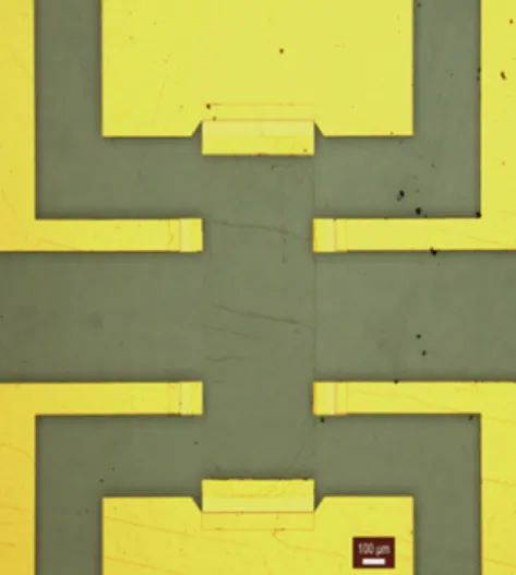
Fig. 1. Optical image of the Hall-bar device patterned on an EG/4H-SiC sample.
2DEG carrier in graphene layers and a 3DEG bulk carrier in the SiC substrate.
(2) At low temperatures, bulk carriers are assumed to be totally frozen. Therefore, the measured Hall carrier density at the lowest temperature is accepted as the temperature-independent 2DEG carrier density.
(3) The change in temperature-dependent measured carrier density is caused by the thermal activation of bulk carriers only.
(4) Densities of bulk carriers and the 2DEG are in the same order.
In the SPCEM calculations, the mobility of a 2D carrier (symbolized as carrier 1) and bulk carrier (symbolized as carrier 2) were calculated by these equations;
(1)
. (2)
In equations , and are Hall carrier densities and Hall mobilities at high magnetic fields and at low magnetic fields, respectively. Temperature-independent 2DEG carrier densities are calculated with at the lowest temperature available. For the bulk carrier density contribution at each temperature step, were used.[18]
The temperature dependence behavior of the Hall mobility and Hall carrier density of the graphene/SiC sample is shown in Fig. 2, measured at a magnetic field of 0.5 Tesla in a temperature range between 1.8 and 300 K. At room temperature, Hall mobility is 1291 cm2/Vs, and Hall sheet carrier densities are 4.4 × 1011 cm−2. On the other hand, at 1.8 K, the Hall mobility of the EG on an SiC sample increases to 7.8 × 103 cm2/Vs and a Hall sheet carrier density decreases to 6.0 × 1010 cm−2. This kind of behavior in nH and µH is
characteristic of the samples that have a dominant conduction of 2DEG.[14,16,18]
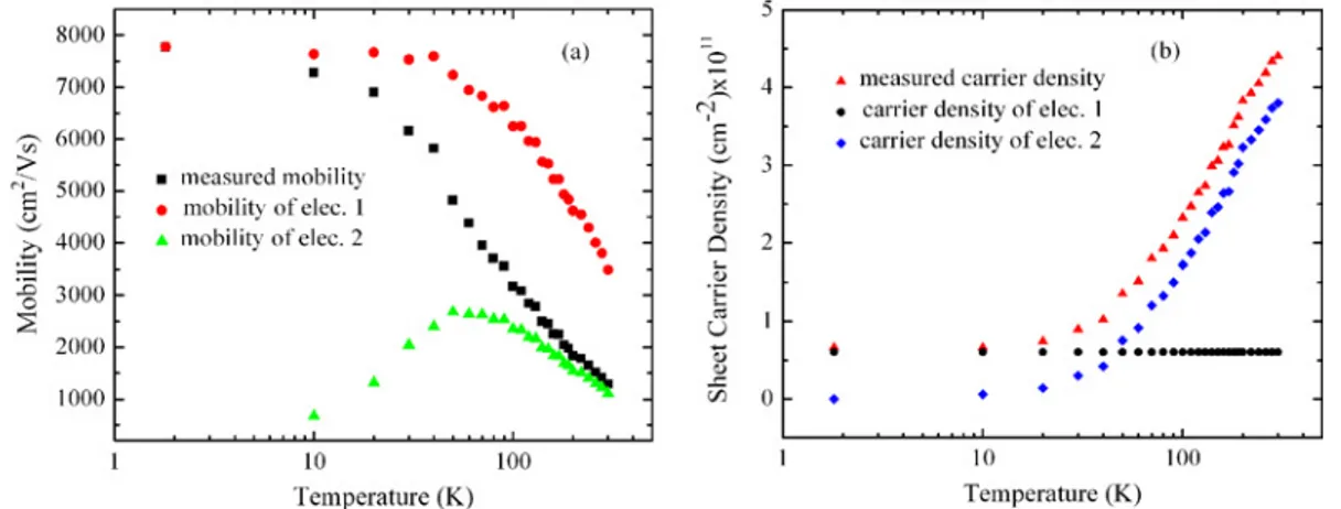
The carrier transports parameters (mobility and carrier density) as a function of temperature that are extracted from the SPCEM procedure are presented in Fig. 3(a) and 3(b), respectively. As clearly indicated by the mobility spectra in Fig. 4(a), two electron carriers are identified in the EG/SiC sample: one high-mobility carrier (7,772 cm2/Vs at 1.8 K and 3,493 cm2/Vs at 300 K) and one low-mobility carrier (1,115 cm2/Vs at 300 K). The data presented in Fig. 4(b) indicates the two different sheet carrier densities. The sheet carrier concentration for electrons in the graphene layers is temperature independent according to assumption #3. However, the sheet carrier concentration in the SiC substrate shows the temperature dependent behavior. The high mobility carrier, which shows the characteristic 2DEG mobility-temperature behavior, has been assigned to the graphene. On the other hand, the second carrier, which contributes much less to the total conductivity, has been assigned to the SiC substrate. We have a 2D gas of high mobility electrons in the graphene layers parallel with much lower mobility electrons µ1 µHLo nH Lo n1LO ---≅ µ2 µHHinH Hi n 1 Hi – nHHi ---≅ µHHin2 Hi nHHi ---= nHHi,µHHi,nHLo µHLo n1LO=nHLO n2LO=nHLO–n1LO
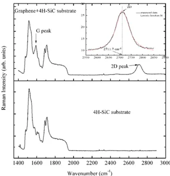
Fig. 2. Raman spectra of EG grown on Si-terminated SiC and 4H-SiC substrate as indicated.
Fig. 3. Temperature dependence of the Hall sheet carrier density (nH), and the Hall carrier mobility (µH), as measured by the Hall effect at
in the SiC substrate layer. The mobility temperature behavior of the second carrier, which is assigned to the SiC substrate, is consistent with the literature data given for 4H-SiC substrate.[20]
Raman spectroscopy is a powerful, fast, and non-destructive method for the characterization of the structural and electronic properties of graphite materials. It gives useful information on the defects (D-band), in-plane vibration of sp2 carbon atoms (G-band), and stacking orders (2D-band).[21-30] The G-band of graphite materials is a doubly degenerate (TO and LO) phonon mode (E2g symmetry) at the
Brillouin zone center, whereas the D-band is due to phonon branches around the K point and requires a defect for its activation.[21,22,23] The evolution of the 2D-band for different graphene sheets has been used for determining the graphene thickness as well as for probing electronic structures through the double resonance process.[28] The symmetry and sharpening of the 2D-band can be used to detect the layer number in graphene.[25,27,28] The electron or hole doping can also be monitored from the stiffening and sharpening of the G-band.[22,30]
Figure 4 shows the Raman spectra of EG + SiC (grown on Si-terminated 4H-SiC) and SiC substrate. The Raman spectrum of the EG + SiC sample has four dominated peaks located at 1,516, 1,592, 1,711, and 2,711 cm−1, of which the peaks at 1,516 and 1,711 cm−1 are from the SiC substrate. The Raman scattering spectra of the EGs samples show the characteristic G and 2D bands on the background of a more or less pronounced signal from the SiC substrate.[29] The
charac-teristic graphene peak at 1,592 cm−1 is the in-plane vibrational G-band, and the 2,711 cm−1 peak is the two-phonon 2D-band.
Significant blue shifts of the G and 2D band were observed in the Raman spectra. The shifted position of the 2D peak at 2,711 cm−1 (compared with the Raman result measured in the micromechanical cleavage graphene layer) indicates the compressive strain of the graphene layer caused by the SiC substrate, during the post-growth cooling down procedure or charge-transfer doping from the substrate.[22,26] Moreover, the tension strain in the graphene precursor will induce a Raman shift to low frequency by approx. 12 cm−1 in the G-peak. Based on a quantitative calculation under biaxial strain,[22,26] the G-peak Raman frequency shift can be defined as where A = −1.44 × 107 cm−2, εxx is
a strain of a graphene layer under biaxial stress σ, ωG0 is the
G-peak Raman frequency of a strain-free graphene and α is a stress coefficient of approx. 7.47 cm−1/GPa. Considering the G-peak position of a strain-free graphene highly-oriented pyrolytic graphite (HOPG) given in the literature as 1,580 cm−1,[26] the Raman frequency difference between the G-peaks of the sample under study and that of the HOPG is approx. 12 cm−1. Therefore, a biaxial stress of 1.61 GPa on EG is obtained. Wang et al.[24] published a detailed investigation on the Raman studies of the monolayer graphene produced by micromechanical cleavage on different substrates, such as standard SiO2 (300 nm)/Si, quartz, Si, glass, NiFe, and
PDMS. They conclude that the Raman features of mono layer graphene are independent of the substrate used and the effect of substrate on the atomic/electronic structures of graphene is negligible. However, they reported a strong blue shift of the G-band Raman spectra of the epitaxial graphene mono layer on the SiC substrate, which were explained by the strain effect caused by the covalent bonding between the SiC substrate and epitaxial graphene, resulting in changes to the lattice constant of graphene.[24] Similar, significant blue shifts of all the Raman peaks were observed in the Raman spectra of the EG grown on SiC substrates by Ni et al..[23] They attributed this significant blue shift to the compressive strain caused by the SiC substrate. And they conclude that, for thicker EG, the strain relaxes and the Raman peaks shift toward those of micromechanical cleavage graphene and graphite.
The 2D peak shape is also used to distinguish single and multilayer samples. The monolayer graphene has a sharp, single 2D peak, in contrast with graphite and multilayer graphene.[22,23,27] In the inset of Fig. 4, the Lorentz function fit to the 2D peak of the Raman spectra of EG is shown. The Lorentzian curve shape of the 2D peak is a feature of epitaxial graphene layers and the signature of a system with a single-band electronic dispersion. The 2D peak is, however, much broader with a full width at half maximum (FWHM) of around 71 cm−1. The broadening can be attributed both to
ωG
∆ =Aεxx/ωG0≈ασ
Fig. 4. Temperature dependence of (a) mobilities and (b) Hall sheet carrier density (nH) of the carriers in SiC substrate and EG layers
defect scattering and two or more layer graphene.[26] Recently, Ferrari et al.[23] demonstrated that the shape of the 2D Raman peak may serve as the fingerprint to distinguish mono-, bi-, and few-layer graphene. The 2D peak stems from a double resonance electron phonon scattering process.[25,27] For mono layer graphene, the 2D peak can be fit to a single Lorentzian curve, whereas the multiple bands in bilayer or few-layer graphene require fitting to four or more Lorentzian curves. Although the Raman data of multilayer epitaxial graphene were recently reported, a similar, clear procedure to differentiate between single layer, bilayer, and multilayer graphene on SiC is lacking.[25,27]
4. CONCLUSIONS
In the present work, in order to extract the conduction effects of 3DEG in the SiC substrate effect, we performed Hall effect measurements in the temperature range 1.8 - 300 K on EG on the SiC substrate. In order to investigate the In graphene layer on the SiC substrate, we have a 2D gas of high mobility (7772 cm2/Vs at 1.8 K and 3493 cm2/Vs at 300 K) electrons in graphene layers parallel with much lower mobility (1115 cm2/Vs at 300 K) electrons in the SiC substrate layer. The high mobility carrier, which shows the characteristic 2DEG mobility-temperature behavior, has been assigned to the 2DEG. On the other hand, the second carrier contributes much less to the total conductivity, and has been assigned to the SiC substrate.
ACKNOWLEDGEMENTS
This work is supported by the projects DPT-HAMIT, ESF-EPIGRAT, EU-N4E, and NATO-SET-181, and TUBITAK under the Project Nos. 107A004, 107A012, and 109E301. One of the authors (E.O.) also acknowledges partial support from the Turkish Academy of Sciences.
REFERENCES
1. K. S. Novoselov, A. K. Geim, S. V. Morozov, D. Jiang, Y. Zhang, S. V. Dubonos, I. V. Grigorieva, and A. A. Firsov, Science 306, 666 (2004).
2. A. K. Geim and K. S. Novoselov, Nature Materials 6, 183 (2007).
3. A. H. C. Neto, F. Guinea, N. M. R. Peres, K. S. Novoselov, and A. K. Geim, Rev. Modern Phys. 81, 109 (2009). 4. F. Rana, IEEE Transactions on Nanotechnology 7, 91 (2008). 5. Y.-M. Lin, K. A. Jenkins, A. Valdes-Garcia, J. P. Small, D.
B. Farmer, and P. Avouris, Nano Lett. 9, 422 (2009). 6. T. Lohmann, K. von Klitzing, and J. H. Smet, Nano Lett. 9,
1973 (2009).
7. J. Hass, W. A. de Heer, and E. H. Conrad, J. Phys.: Con-dens. Matter 20, 323202 (2008).
8. K. I. Bolotin, K. J. Sikes, J. Hone, H. L. Stormer, and P. Kim, Phys. Rev. Lett. 101, 096802 (2008).
9. F. Varchon, R. Feng, J. Hass, X. Li, B. Ngoc Nguyen, C. Naud, P. Mallet, J.-Y. Veuillen, C. Berger, E. H. Conrad, and L. Magaud, Phys. Rev. Lett. 99, 126805 (2007). 10. X. Li, W. Cai, J. An, S. Kim, J. Nah, D. Yang, R. Piner, A.
Velamakanni, I. Jung, E. Tutuc, S. K. Banerjee, L. Colombo, and R. S. Ruoff, Science 324, 1245 (2009).
11. K. S. Kim, Y. Zhao, H. Jang, S. Y. Lee, J. M. Kim, K. S. Kim, J.-H. Ahn, P. Kim, J.-Y. Choi, and B. H. Hong, Nature 457, 706 (2009).
12. M. J. Kane, N. Apsley, D. A. Anderson, L. L. Taylor, and T. Kerr, J. Phys. C: Solid State Phys. 18, 5629 (1985). 13. W. A. Beck and J. R. Anderson, J. Appl. Phys. 62, 541 (1987). 14. Z. Dziuba, J. Antoszewski, J. M. Dell, L. Faraone, P. Kozo-doy, S. Keller, B. Keller, S. P. DenBaars, and U. K. Mishra, J. Appl. Phys. 82, 2996 (1997).
15. I. Vurgaftman, J. R. Meyer, and C. A. Hoffman, D. Red-fern, J. Antoszewski, L. Faraone, and J. R. Lindemuth, J. Appl. Phys. 84, 4966 (1998).
16. S. B. Lisesivdin, A. Yildiz, N. Balkan, M. Kasap, S. Ozce-lik, and E. Ozbay, J. Appl. Phys. 108, 013712 (2010). 17. C. Mavroidis, J. J. Harris, R. B. Jackman, I. Harrison, B. J.
Ansell, Z. Bougrioua, and I. Moerman, J. Appl. Phys. 91, 9835 (2002).
18. S. B. Lisesivdin, N. Balkan, and E. Ozbay, Microelectron-ics J. 40, 413 (2009).
19. A. Yildiz, S. B. Lisesivdin, M. Kasap, S. Ozcelik, E. Ozbay, and N. Balkan, Appl. Phys. A 98, 557 (2010). 20. M. Roschke and F. Schwierz, IEEE Transactions on
Elec-tron Devices 48, 1442 (2001).
21. F. Tuinstra and J. L. Koenig, J. Chem. Phys. 53, 1126 (1970).
22. L. M. Malard, M. A. Pimenta, G. Dresselhaus, and M. S. Dresselhaus, Physics Reports 473, 51 (2009).
23. A. C. Ferrari, J. C. Meyer, V. Scardaci, C. Casiraghi, M. Lazzeri, F. Mauri, S. Piscanec, D. Jiang, K. S. Novoselov, S. Roth, and A. K. Geim, Phys. Rev. Lett. 97, 187401 (2006). 24. Y. Y. Wang, Z. H. Ni, T. Yu, Z. X. Shen, H. M. Wang, Y. H. Wu, W. Chen, and A. T. S. Wee, J. Phys. Chem. C 112, 10637 (2008).
25.C. Faugeras, A. Nerrière, M. Potemski, A. Mahmood and E. Dujardin, C. Berger, and W. A. deHeer, Appl. Phys. Lett. 92, 011914 (2008).
26. Z. H. Ni, W. Chen, X. F. Fan, J. L. Kuo, T. Yu, A. T. S. Wee, and Z. X. Shen, Phys.Rev. B 77, 115416 (2008). 27. J. Röhrl, M. Hundhausen, K. V. Emtsev, Th. Seyller, R.
Graupner, and L. Ley, Appl. Phys. Lett. 92, 201918 (2008). 28. Z. H. Ni, H. M. Wang, J. Kasim, H. M. Fan, T. Yu, Y. H. Wu, Y. P. Feng, and Z. X. Shen, Nano Lett. 7, 2758 (2007). 29. J. C. Burton, L. Sun, F. H. Long, Z. C. Feng, and I. T.
Fer-guson, Phys. Rev. B 59, 7282 (1999).
30. C. Casiraghi, S. Pisana, K. S. Novoselov, A. K. Geim, and A. C. Ferrari, Appl. Phys. Lett. 91, 233108 (2007).