Nanoscale charging hysteresis measurement by multifrequency
electrostatic force spectroscopy
Umut Bostanci,1,a兲 M. Kurtuluş Abak,2O. Aktaş,2and A. Dâna2,b兲 1
Department of Physics, Middle East Technical University, 06531 Ankara, Turkey
2Institute of Materials Science and Nanotechnology, Bilkent University, 06800 Ankara, Turkey 共Received 2 November 2007; accepted 7 February 2008; published online 4 March 2008兲 We report a scanning probe technique that can be used to measure charging of localized states on conducting or partially insulating substrates at room temperature under ambient conditions. Electrostatic interactions in the presence of a charged particle between the tip and the sample is monitored by the second order flexural mode, while the fundamental mode is used for stabilizing the tip-sample separation. Cycling the bias voltage between two limits, it is possible to observe hysteresis of the second order mode amplitude due to charging. Results are presented on silicon nitride films containing silicon nanocrystals. © 2008 American Institute of Physics.
关DOI:10.1063/1.2888765兴
Atomic force microscopy共AFM兲1is a powerful tool for imaging various tip-sample interactions on the nanometer scale. Imaging electronic properties are especially important for nanoelectronics; and electrostatic force microscopy has been applied to, for example, electrical characterization of carbon nanotubes,2DNA,3and nanoparticles.4 Kelvin probe microscopy, which measures the contact potential difference between the tip and the sample, was applied to the label-free detection of nucleotides.5Electrostatic force microscopy has been used to study light induced carrier dynamics in organic conductors.6 Single carrier charging events have been ob-served by AFM.7,8 Recently, multifrequency imaging has been applied to imaging of electrostatic forces on insulating substrates.9
In this letter, we report an extension of multifrequency AFM to a spectroscopy technique similar to capacitance spectroscopy. We refer to the technique as the multifre-quency electrostatic force spectroscopy共MFEFS兲. The tech-nique is demonstrated by observing charging hysteresis of silicon nanocrystals in a silicon nitride matrix on silicon. In the experiments, a commercial AFM tip was used. The tip was a Pt/Ir coated rectangular cantilever with a nominal length of L = 220m, width of w = 30m, tip height of H = 15m, tip half-cone angle of= 15°, and nominal tip ra-dius of R = 15 nm. The fundamental mode of the cantilever is used to stabilize the average tip-sample separation, and the second order mode is used to resonantly measure electro-static forces. In order to limit the charge transfer between the biased tip and the surface, and to avoid instabilities during tapping, the tip is coated with a nominal td= 10 nm thick
Si3N4layer in a plasma-enhanced chemical-vapor deposition 共PECVD兲 reactor 共PlasmaLab 8510C兲 using SiH4 and NH3 as precursor gases. This layer is analogous to the gate oxide in flash memory devices, and the tip can be considered as a metallic gate. The first and second eigenfrequencies of the cantilever were measured to be f0⬵70.01 kHz and f2 ⬵448.83 kHz, with quality factors of Q0= 220 and Q2= 450. The experiments were performed on a commercial AFM sys-tem 共PSIA XE100E兲 under ambient conditions. During im-aging, the cantilever is driven at a frequency slightly below
f0by the dither piezo, and a sinusoidal voltage superimposed on a dc voltage is applied at a frequency that coincides with the second order flexural mode frequency2= 2f2. The de-flection of the second-order mode is measured using an ex-ternal rf lock-in amplifier 共Stanford Research Systems SR844兲. It is known that, unless the second order mode quency is an integer multiple of the fundamental mode fre-quency, tapping at the fundamental frequency does not gen-erate significant oscillation of the second order mode.10,11 Using this fact and separate excitation sources for the two modes, it is possible to separate short and long range inter-actions by measuring the oscillation amplitudes and phase at f0 and f2. In order to minimize the coupling of the two modes to each other through nonlinearities imposed by the tip-sample interaction, the second order mode amplitude A2 was kept below 1 nm. Topographic feedback is maintained by the feedback loop of the AFM system using the funda-mental mode. Typical fundafunda-mental mode amplitudes were A0⯝10–20 nm defined by the adjustable set point. The tip-sample interaction force can be written as the sum of elec-trostatic and nonelecelec-trostatic terms as Fts= Fe+ Fne. The electrostatic component is dependent on the tip-sample bias Vts. In our experiments, the tip-sample voltage Vts is of the form Vts共t兲=Vdc+ Vaccos共2t兲, Vac typically being about 0.1 to 1 V. This modulated bias results in an average elec-trostatic force amplitude Fe,2 at frequency f2 that can be written as
Fe,2=
冓
Cts共z兲z
冔
共Vdc− Vcpd兲Vac, 共1兲 where Cts共z兲 is the tip-sample capacitance, Vdc is the tip-sample bias, and VCPD is the contact potential difference. Brackets denote averaging over the oscillation period. When the ac excitation amplitude Vacis kept constant, Fe,2islin-early proportional to Vdc− VCPD.
In order to verify that the second order mode oscillation is excited primarily by electrostatic interactions, we sweep the dc bias or the frequency of Vac and record the second order mode amplitude and phase, while the first order mode is tapping a flat and clean silicon surface. The excitation amplitude of the second order mode follows the dc voltage bias, and is nulled when the contact potential difference is a兲Electronic mail: [email protected].
b兲Electronic mail: [email protected].
APPLIED PHYSICS LETTERS 92, 093108共2008兲
0003-6951/2008/92共9兲/093108/3/$23.00 92, 093108-1 © 2008 American Institute of Physics
compensated around −0.3 V, as seen in Fig.1, in accordance with Eq.共1兲. For large biases, detachment of the tip from the sample surface takes place. This effect is previously well studied and can be understood by considering the coupling of the dc electrostatic forces to the topography channel.12 Tip retraction results in a reduced average electrostatic excitation of the second order mode, due to the increased average tip-sample separation. The feedback effect explains the observed deviation from linearity in the excitation amplitude at bias differences greater than 0.5 V shown in Fig.1. This effect must be avoided or be carefully considered when quantita-tive measurements under large biases are needed.
If a localized state is separated from the bulk of the substrate by a tunnel barrier, applying an electric field large enough to make the tunnel barrier transparent for carrier transport will result in accumulated charge in the localized state. When the field is reduced, the carriers will stay in the localized state until they slowly tunnel out, or a large enough reverse polarity field causes them to escape. In order to in-terpret the data collected during a measurement of localized charging, the electrostatic model has to include the effect of localized charges. For the sake of simplicity, we consider the case of a nanocrystal below the tip. The electrostatic interac-tion energy between the tip and the sample with a charge trapped in a nanocrystal in between is given by13,14
U = q 2 2Ct − C1 2Ct qV −C1C2 2Ct V2−C0 2 V 2, 共2兲
where C0 is the tip-substrate capacitance, C1 is the tip-nanocrystal capacitance, C2 is the nanocrystal-substrate
ca-pacitance, and Ct= C1+ C2total capacitance seen by the tip. The electrostatic force can be obtained from Eq.共2兲 by dif-ferentiation with respect to the tip-sample separation z,
Fe= 1 Ct C1 z
冉
q2 2 − C2qV + C22V2 2冊
+ 1 2 C0 z V 2. 共3兲Using Eq. 共3兲, and the ac modulated bias, different fre-quency components of the electrostatic force can be evalu-ated. When the electrostatic excitation is measured as a func-tion of the bias, the presence of charge in a state between the tip and the sample results in a shift of the curve along the bias coordinate. Using algebraic manipulation, Eq.共3兲can be used to calculate the hysteresis between the force-voltage curves with a charge q deposited in between the two curves, given by ⌬VH= q C2
冋
1 +C0 z冒
冉
C2 C1+ C2冊
2C 1 z册
−1 . 共4兲The voltage⌬VHis the charging voltage of the trap Vc
= q/C2, divided by a dimensionless factor that quantifies the shielding effect of the tip. Using Eq.共4兲, by measuring the hysteresis at specific location, information about the local density of states and charging-discharging dynamics can be obtained. The technique was demonstrated on different sets of samples. Figure2共a兲shows the typical result for the am-plitude of the second order mode during the cyclic voltage sweep on a clean silicon surface. No hysteresis can be ob-served, due to the low density of surface states on a clean silicon surface. Figure 2共b兲 shows the typical result of the same experiment performed on a 10 nm thick silicon nitride film with embedded silicon nanocrystals grown by PECVD 共see supporting information兲. The average diameter of silicon nanocrystals is 5 nm inferred from photoluminescence mea-surements. Significant hysteresis of about 310 mV can be observed. Assuming a nominal nanocrystal diameter of 5 nm and a nominal conducting tip radius of 15 nm, through finite element analysis, the relevant capacitances and gradients are estimated as C1= 1.05 aF, C2= 1.4 aF, C0/z = 120 pF/m, andC1/z = 25 pF/m. These values give a hysteresis volt-age of 56 mV per electron per nanocrystal. The measured hysteresis of 310 mV corresponds to about six electrons per nanocrystal, deposited between 0 and 2 V. Arrows in Fig. FIG. 1. 共Color online兲 Dependence of the amplitude of the second order
mechanical mode on dc bias voltage, during tapping with the fundamental mode. The ac frequency was on resonance with the second order mode. Smooth transition of the phase of the oscillation indicates finite capacitive coupling of the drive signal to the dither piezo.
FIG. 2.共Color online兲 Electrostatic excitation of the second order mode during a voltage sweep on a clean silicon surface. The arrows denote voltage sweep directions. No hysteresis can be observed.共b兲 Electrostatic excitation of the second order mode during a voltage sweep on silicon nitride layer with silicon nanocrystals embedded. Significant hysteresis is observable, indicating charging of nanocrystals. The arrows denote onset of charging and discharging events. The insets show capacitance-voltage traces of macroscopic capacitors fabricated using silicon nitride films without and with nanocrystals.
093108-2 Bostanci et al. Appl. Phys. Lett. 92, 093108共2008兲
2共b兲 denote onset of charging and discharging of the nano-crystals. For our signal to noise ratio, single electron events should be observable for nanoparticles with up to 10 nm di-ameter, 3 nm away from the substrate, and using a 15 nm radius tip. The exact hysteresis value for a single electron depends on other parameters of the sample such as the thick-ness and dielectric constant of the tunnel barrier. In order to highlight the analogy of MFEFS with conventional capaci-tance spectroscopy, macroscopic capacitors 共1 mm gate di-ameter兲 were fabricated on nonstoichiometric silicon nitride films containing nanocrystals and on stoichiometric silicon nitride films without nanocrystals. The capacitance-voltage traces shown in the insets of Figs.2共a兲and2共b兲are acquired using an LCR meter and display similar hysteresis.
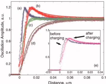
In order to ensure that the observed effects are due to charging and not due to instability caused by tip-sample in-teractions, it is necessary to investigate the tip-sample inter-actions in greater detail. Figure3 shows amplitude-distance data obtained at different biases. The inset of Fig.3 shows that long-range electrostatic interactions are indeed perturbed as a result of charging of the film. Amplitude distance curves obtained at zero bias differ before and after charging. The effect of charging is roughly equivalent to applying a bias ⌬VHto the cantilever. The observations are well understood
by considering the cantilever dynamics taking into account the electrostatic and nonelectrostatic interactions. Numerical calculations of how the oscillation amplitude of the funda-mental resonant mode changes with bias and tip-sample separation is shown as solid curves in Fig.3. Measurement results and simulation results of the tip-sample interaction indicate that, in the repulsive mode, the amplitude distance curves are single valued for tip-sample separations below the free oscillation amplitude. For drive frequencies below the zero-bias resonant frequency, peaking of the amplitude can be observed if the tip-sample separation is greater than the
free oscillation amplitude. For stable operation of MFEFS, this parameter range must be avoided and amplitude set point of topographic feedback must be chosen below 90 percent of free oscillation amplitude. For drive frequencies above zero-bias resonant frequency, there is no peaking that may poten-tially result in bistabilities. However, in this parameter range, coupling of the electrostatic interactions to the topography feedback are more pronounced. There are advantages of the MFEFS technique to force or amplitude versus distance mea-surements. In MFEFS, the tip is never brought into hard contact with the sample, therefore both the sample and the tip structures are preserved. In conventional force versus dis-tance measurements, instrument drifts are not independently compensated; however, MFEFS inherently stabilizes the tip-sample separation. Bias sweeps in a conventional force ver-sus distance measurement requires complicated data analy-sis, whereas MFEFS data directly give a hysteresis voltage that can be related to charging through characterization of the tip shape. Ideally, MFEFS measurements can be done rapidly共about Q2/ f2⬇1 ms per bias point兲, therefore, spatial drifts of instrumentation can have less effect on measure-ments.
The MFEFS technique we presented here can be applied using a standard AFM system using a standard metal coated cantilever in ambient conditions. For conductive substrates and samples without a cap layer, a thin barrier coating on the tip can be applied to improve stability. The technique can be regarded as a technique that is similar to scanning tunneling spectroscopy 共STS兲 used in scanning tunneling microscopy studies. However, it can be used to study trap levels on par-tially insulating samples where STS can not be applied. De-tailed description of excitation of the second order mode by ac electrostatic force; Finite element calculation results of tip-nanocrystal and nanocrystals substrate capacitances; Preparation of silicon nitride films containing silicon nano-particles can be found in the supporting information.
This work has been partially funded by Tübitak Grant 104T520 and 107T547, and by funding from the State Plan-ning Agency of the Turkish Republic. Aykutlu Dâna thanks Atilla Aydinli for letting use of the capacitance measurement setup.
1G. Binnig, C. F. Quate, and C. Gerber,Phys. Rev. Lett. 56, 930共1986兲. 2T. S. Jespersen and J. Nygard,Nano Lett. 5, 1838共2005兲.
3M. Bockrath, N. Markovic, A. Shepard, and M. Tinkham,Nano Lett. 2,
187共2002兲.
4R. M. Nyffenegger, R. M. Penner, and R. Schierle,Appl. Phys. Lett. 71,
13共1997兲.
5A. K. Sinensky and A. M. Belcher,Nat. Nanotechnol. 2, 653共2007兲. 6D. C. Coffey and D. S. Ginger,Nat. Mater. 5, 735共2006兲.
7A. Dâna and Y. Yamamoto,Nanotechnology 16, S125共2005兲. 8E. Bussmann and C. C. Williams,Appl. Phys. Lett. 88, 263108共2006兲. 9R. W. Stark, N. Naujoks, and A. Stemmer,Nanotechnology 18, 065502
共2007兲.
10R. W. Stark and W. M. Heckl,Surf. Sci. 457, 219共2000兲.
11O. Sahin, C. F. Quate, O. Solgaard, and A. Atalar, Phys. Rev. B 69,
165416共2004兲.
12D. Ziegler, J. Reichen, N. Naujoks, and A. Stemmer, Nanotechnology 18,
225505共2007兲.
13D. M. Schaadt, E. T. Yu, S. Sankar, and A. E. Berkowitz,Appl. Phys. Lett.
74, 472共1999兲.
14Y. Azuma, M. Kanehara, T. Teranishi, and Y. Majima,Phys. Rev. Lett. 96,
016108共2006兲. FIG. 3.共Color online兲 Oscillation amplitude vs tip-sample separation. When
the cantilever is driven below its resonance frequency, peaking of the oscil-lation amplitude is observed共a兲 for 0 V bias and 共b兲 for 2 V bias. If the drive frequency is above the resonance frequency, no such peaking occurs as seen in共c兲 for 0 V bias and 共d兲 for 2 V bias. Representative theoretical fits obtained by using the same set of parameters and by only changing the bias parameter are shown as solid curves. 共e兲 The inset shows amplitude vs tip-sample separation scans obtained at 0 V bias before and after charging the film by contacting with a 2 V biased tip. Shift of the curve and broad-ening of the peak after charging indicate a local surface potential shift.
093108-3 Bostanci et al. Appl. Phys. Lett. 92, 093108共2008兲