Asymmetric light propagation in chirped
photonic crystal waveguides
H. Kurt,1,* D. Yilmaz,1 A. E. Akosman,2 and E. Ozbay2
1Department of Electrical and Electronics Engineering TOBB University of Economics and Technology, 06560 Ankara, Turkey
2Department of Electrical and Electronics Engineering, Nanotechnology Research Center, Bilkent University, 06800 Ankara, Turkey
*
Abstract: We report numerical and experimental investigations of
asymmetric light propagation in a newly designed photonic structure that is formed by creating a chirped photonic crystal (PC) waveguide. The use of a non-symmetric distribution of unit cells of PC ensures the obtaining of asymmetric light propagation. Properly designing the spatial modulation of a PC waveguide inherently modifies the band structure. That in turn induces asymmetry for the light’s followed path. The investigation of the transmission characteristics of this structure reveals optical diode like transmission behavior. The amount of power collected at the output of the waveguide centerline is different for the forward and backward propagation directions in the designed configuration. The advantageous properties of the proposed approach are the linear optic concept, compact configuration and compatibility with the integrated photonics. These features are expected to hold great potential for implementing practical optical rectifier-type devices.
©2012 Optical Society of America
OCIS codes: (130.5296) Photonic crystal waveguides; (230.5298) Photonic crystals;
(130.0130) Integrated optics; (120.7000) Transmission.
References and links
1. M. Scalora, J. P. Dowling, C. M. Bowden, and M. J. Bloemer, “The photonic band edge optical diode,” J. Appl. Phys. 76(4), 2023–2026 (1994).
2. M. D. Tocci, M. J. Bloemer, M. Scalora, J. P. Dowling, and C. M. Bowden, “Thin film nonlinear optical diode,” Appl. Phys. Lett. 66(18), 2324–2326 (1995).
3. F. Biancalana, “All-optical diode action with quasiperiodic photonic crystals,” J. Appl. Phys. 104(9), 093113 (2008).
4. A. E. Serebryannikov, “One-way diffraction effects in photonic crystal gratings made of isotropic materials,” Phys. Rev. B 80, 155117 (2009).
5. A. O. Cakmak, E. Colak, A. E. Serebryannikov, and E. Ozbay, “Unidirectional transmission in photonic-crystal gratings at beam-type illumination,” Opt. Express 18(21), 22283–22298 (2010).
6. M. J. Lockyear, A. P. Hibbins, K. R. White, and J. R. Sambles, “One-way diffraction grating,” Phys. Rev. E Stat. Nonlin. Soft Matter Phys. 74(5), 056611 (2006).
7. W.-M. Ye, X.-D. Yuan, C.-C. Guo, and C. Zen, “Unidirectional transmission in non-symmetric gratings made of isotropic material,” Opt. Express 18(8), 7590–7595 (2010).
8. Z. Yu, G. Veronis, Z. Wang, and S. Fan, “One-way electromagnetic waveguide formed at the interface between a plasmonic metal under a static magnetic field and a photonic crystal,” Phys. Rev. Lett. 100(2), 023902 (2008). 9. Z. Wang, Y. Chong, J. D. Joannopoulos, and M. Soljacić, “Observation of unidirectional backscattering-immune
topological electromagnetic states,” Nature 461(7265), 772–775 (2009).
10. H. Takeda and S. John, “Compact optical one-way waveguide isolators for photonic-band-gap microchips,” Phys. Rev. A 78(2), 023804 (2008).
11. Z. Yu and S. Fan, “Complete optical isolation created by indirect interband photonic transitions,” Nat. Photonics
3(2), 91–94 (2009).
12. X.-F. Li, X. Ni, L. Feng, M.-H. Lu, C. He, and Y.-F. Chen, “Tunable Unidirectional Sound Propagation through a Sonic-Crystal-Based Acoustic Diode,” Phys. Rev. Lett. 106(8), 084301 (2011).
13. Z. He, S. Peng, Y. Ye, Z. Dai, C. Qiu, M. Ke, and Z. Liu, “Asymmetric acoustic gratings,” Appl. Phys. Lett.
98(8), 083505 (2011).
14. C. Wang, C.-Z. Zhou, and Z. Y. Li, “On-chip optical diode based on silicon photonic crystal heterojunctions,” Opt. Express 19(27), 26948–26955 (2011).
15. S. Johnson and J. Joannopoulos, “Block-iterative frequency-domain methods for Maxwell’s equations in a planewave basis,” Opt. Express 8(3), 173–190 (2001).
16. A. F. Oskooi, D. Roundy, M. Ibanescu, P. Bermel, J. D. Joannopoulos, and S. G. Johnson, “MEEP: A flexible free-software package for electromagnetic simulations by the FDTD method,” Comput. Phys. Commun. 181(3), 687–702 (2010).
1. Introduction
The importance of diode-like behavior obtained for optical pulses has initiated a lot of research activity in the photonics area [1–11]. Even though it is relatively easy to route and confine light in photonic platforms by means of index and band gap guiding, great difficulties arise when implementing rectifier-type electromagnetic wave propagation due to the reciprocal behavior of optical waveguides. Controlling the direction of light propagation in terms of one-way is of significant importance due to the optical analogue of the well known and widely used electronic diode. When the polarity of the electric signal changes from positive to negative, the diode blocks the signal propagation. In a similar fashion, the direction of light determines which way the optical pulse is allowed to pass through. Compact and efficient (producing good optical isolation) approaches are required to obtain the possibility of having a practical device. In the ideal case, one-way wave propagation should allow light to travel from one side to the other in the forward direction but the transmission should be inhibited in the backward direction.
The early approaches have adapted different methods to obtain one-way light propagation, i.e., break the time-reversal symmetry of the system. However, most of the time, either material nonlinearity is employed or metallic/magnetic-optical materials are required in the majority of the proposed solutions [1–3, 8–11]. Nonlinear approaches require high-power input sources due to a small nonlinear susceptibility coefficient and metal inclusion accompanies optical losses that diminish light propagation. In spite of these approaches, there might be intermediate solutions that can provide partial realization of one-way propagation. For example, recent studies have attempted to manipulate the light propagation direction by assigning asymmetric dielectric corrugations (gratings). The creation of higher side lobes (for example ±1 diffraction orders) may suppress the 0th order (main lobe) for asymmetric light propagation. For the opposite direction, only the main lobe emerges without any accompanying higher order lobes [4–7]. As a result, asymmetric light propagation can be achieved not only for electromagnetic waves but also for acoustic waves [12, 13]. The acoustic wave counterpart of unidirectional propagation is achieved using sonic crystals and asymmetric acoustic gratings in Refs [12]. and [13], respectively. The directional band gap difference of a hetero-junction structure based on square-lattice photonic crystals was proposed to implement unidirectional optical diode action in Ref [14].
Traditional approaches for obtaining non-reciprocity dictates breaking time-reversal symmetry. In dielectric structures, the dispersion diagram obeys the relationω
( )
k =ω(
−k)
, where k is the wave vector. In the present study, we show that we can achieve asymmetric light propagation by using a chirped photonic crystal waveguide (PCW). Regular PCW can be realized by using a periodic dielectric medium known as photonic crystals [15]. To obtain a waveguide, one should introduce a line-defect such that the unit cells’ shape or size along a certain direction must be perturbed. The manipulation of the waveguide mode is achieved by engineering the spatial distribution of unit cells. Field profiles are calculated to elucidate asymmetric light propagation characteristics of chirped PCW. The wave propagating from left to right and right to left behaves differently. In other words, the transmitted power characteristics become strongly dependent on the direction of the incidence of light.Since no nonlinear optics concept or anisotropic material is utilized, the approach is fairly practical to implement. Thanks to the special path that optical pulses follow in the designed structure, we show the asymmetric light propagation. We demonstrate that the optical response of chirped PCW holds great promise for performing asymmetric light propagation. The experimental demonstration is carried out at microwave frequencies and good agreement between the calculated and experimentally measured results were obtained.
Fig. 1. Schematic presentation of asymmetric light propagation mechanism occurring in chirped photonic crystal waveguide.
Figure 1 shows a pictorial version of two-dimensional photonic structure that provides asymmetric light propagation. One can consider two scenarios. For the first scenario, when A acts as an input source for the left-to-right transmission, D becomes zero and the non-zero parts are B, E and C. The meaningful signal appears in C due to the fact that B corresponds to total reflected light and E denotes leakage light. B and E can be assumed as loss. For the opposite direction excitation (right-to-left) that is the second scenario, D illuminates the device and A is zero. In this case, the meaningful signal appears in B because C represents reflected light and E denotes the leakage light. For the opposite propagation direction, B and C are different in terms of spatial field profiles and total collected power. Because different leakage power in port E occurs and the reflected fields are different for each case.
2. Proposed optical diode-like structure
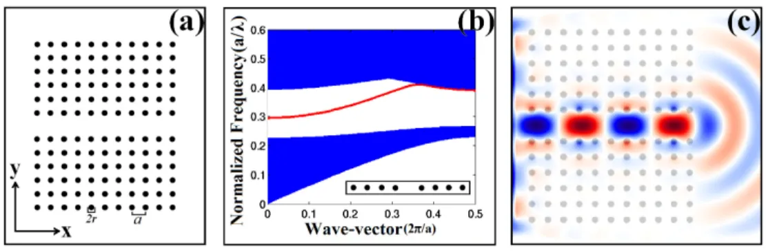
The basic ingredient of the optical diode structure in our case is a regular square-lattice PC waveguide whose structural parameters are presented in Fig. 2(a). The radii of the rods are 0.22a and refractive index equals to 3.46. The lattice constant is represented by a. One row of rods along the ΓΧdirection are omitted to induce a single mode waveguide. The numerical analysis is only carried out for TM polarization (electric field is perpendicular to the x-y plane). The spatial profiles of the forward and backward transmitted powers are expected to overlap due to the reciprocal nature of the waveguide structure. This expectation can be easily validated by inspecting the dispersion diagram in Fig. 2(b) that is obtained by the plane wave expansion method [15]. The waveguide mode is even with respect to k-axis and it spans a broad range of frequencies. Figure 2(c) corresponds to the incidence case that has the source at the left side of the structure. Repeating the same calculation by positioning the source at the right side will yield exactly the same field pattern at the exit area (result is not shown). Hence, there is no optical diode action. That means the structure does not differentiate the propagation direction of the incident wave. Light propagation at a frequency corresponding to the waveguide mode within the band gap region easily propagates in both directions and the amount of transmitted power in the opposite directions is exactly the same.
Fig. 2. (a) Schematic of a regular photonic crystal waveguide. (b) The dispersion diagram of regular photonic crystal waveguide. (c) Incident light propagation from left-to-right in the waveguide structure.
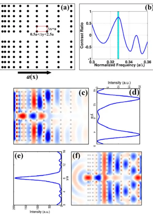
To break the structural symmetry, we purposely introduced a distance increment between each neighboring column of the dielectric rods. Figure 3(a) schematically describes the followed approach. While the distance between each unit cell is kept at a along the y-direction ( y∆ =a), the separation of rods along the x-direction linearly increases as denoted bya x
( )
. The total length of the chirped PCW is approximately 16a long and the distance modulation occurs within 0.50a and 2.50a. We performed numerical studies based on the two-dimensional finite-difference time-domain method [16]. The first step is to check if there is a lack of similarity in the transmission.Figure 3(b) presents the contrast ratio that defines the normalized difference between the two oppositely propagated wavesT =(T−xˆ−T+xˆ) (T−xˆ+T+xˆ), where T−ˆxand T+ˆxrepresent
transmission power propagating along -x (right-to-left) and + x (left-to-right) directions, respectively. The difference between the two opposite transmissions is the cause of asymmetric power collection. The inspection of the graph reveals the frequency region that is appropriate for asymmetric light propagation. We selected the operating frequency as
0.3288
a λ = because the highest transmission efficiency is observed at that frequency. Figures 3(c) and 3(f) present the time domain snapshots of light propagations for two different incidence directions. The electric field profiles across the transverse cross-sections of the two cases are presented in Figs. 3(d) and 3(e). There are important observations that can be concluded from these figures. While the electric field propagates along the + x direction, and the guiding of light is lost towards the end of the structure. As a result, field leakage leaves weak field amplitude at the optical axis. The transmission is partially blocked at the front side of the structure except the waveguide region. In the case where the reverse propagation takes place, the field follows a similar path, and both components propagating along the central part and side areas combine at the middle section of the structure (close to the exit side). That yields a strong electric field appearance at the other side for the –x propagation direction. The electric field profiles support asymmetric light propagation mechanism as shown in Figs. 3(c)-3(f).
Fig. 3. (a) A photonic crystal waveguide that has linearly increased the distance separation between each neighboring column of rods. (b) The spectral content of the contrast ratio. The blue rectangle designates the selected frequency value. (c) Time-domain snapshot of propagation of light from left to right. (d) The transverse field profile across the end face of the structure. (e) The transverse field profile across the front side of the structure. (f) Time-domain snapshot of light propagation from right to left.
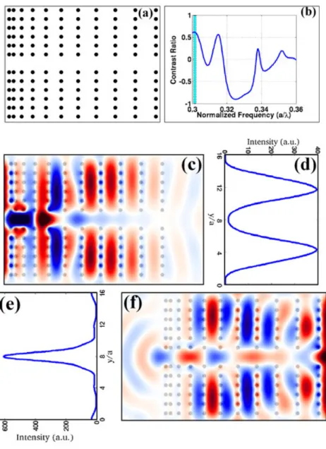
In another design attempt for a chirping parameter, the distance between each neighboring column of rods is increased in a parabolic pattern as shown in Fig. 4(a). Again as before, the structure is kept intact along the y-direction. The total length of the chirped PCW is 16.89a long. The consequence of this modification is the pronounced contrast peaks appearing in the optical response. Figure 4(b) corresponds to the contrast ratio of the two opposite directions. By inspecting the figure, we selected the operating frequency asa λ =/ 0.2992. The electric
field snapshots for the two directions are presented in Figs. 3(c) and 3(f). The cross-section profiles of E-fields at the two sides of the structure produces two strong side lobes with absence of the main lobe at the optic axis. On the other hand, a complementary field profile occurs for the opposite direction. The strong electric field emerges with the absence of side lobes. The amplitude comparison of two cases reveals the suppression of light propagation for one direction while supporting and promoting it for the opposite direction. Consequently, asymmetric power transmission for the opposite directions is achieved.
Fig. 4. (a) Another chirped photonic crystal waveguide is shown. The distance between each neighboring column of rods increased in a parabolic pattern. (b) The spectral content of the contrast ratio. The blue rectangle designates the selected frequency value. (c) Time-domain snapshot of propagation of light from left to right. (d) The transverse field profile across the end face of the structure. (e) The transverse field profile across the front side of the structure. (f) Time-domain snapshot of propagation of light from right to left.
When a comparison is made between linear and quadratic chirpings of lattice distance along the x-direction, we infer from the FDTD results that, a similar wave propagation
mechanism is valid for both cases. The quadratic chirping produces a higher contrast ratio (the ratio of intensity values at the waveguide centerline).
3. Discussions and physical explanation of asymmetric light propagation
In principle, an electronic diode is a nonlinear circuit element. The electric-current flow only occurs under the forward biasing case of the terminals while the reverse-direction flowing of the current is inhibited. The concept of allowing light to be a propagating wave only along one direction and inhibiting for the opposite direction carries huge potential in the optical processing of information. While this is the case for ideal solutions that break reciprocity, here we propose a partial solution that keeps reciprocity.
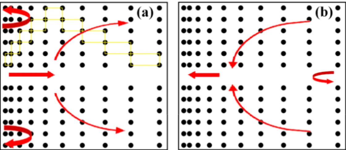
Fig. 5. Schematic representation of a chirped photonic crystal waveguide that enables light’s asymmetric propagation is provided. (a) and (b) correspond to left-to-right and right-to-left propagation, respectively. Yellow boxes in (a) show unit cell variations along the propagation direction.
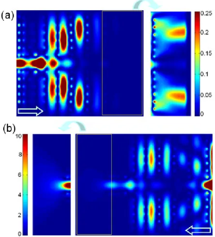
Figure 5 demonstrates the flow of light in each direction. The red arrows highlight the path of the field’s major component. Starting from the left side of the structure as shown in Fig. 5(a), first the incident light mainly travels at the center. After propagating a few lattice distance, the electric field starts to leak towards the y-direction. The structure becomes sparse along the x-direction and lattice spacing is kept constant along the y-direction. Consequently, after the leakage of the field, it begins to travel again along the x-direction and reaching the end of the structure. The chirping of lattice distance induces the loss of a waveguide effect along the centerline. The propagation of light from the right-to-left direction is schematically presented in Fig. 5(b). The central lobe strongly appears at the waveguide exit. The close inspection of the intensity distribution provided in Fig. 6 for linearly chirped case supports the above explanation. For the forward direction shown in Fig. 5(a), the amount of light reaching the waveguide centerline is very small as compared to the backward propagation case that is presented in Fig. 6(b). The end sections of Figs. 6(a) and 6(b) are re-plotted to easily visualize field distributions.
Fig. 6. The detailed presentations of the intensity distributions in linearly chirped waveguide configuration for the forward and backward light propagations are shown in (a) and (b), respectively.
The discrimination of the light propagation direction occurs due to the asymmetric waveguide configuration. The light is mainly confined at the first section of the structure. As we increase the separation, and thereby reduce the filling factor, then the waveguide mode moves towards the outside of the band gap. Then light starts to leak out and leaves an almost null-field at the central part of the waveguide. There are two strong side lobes collecting the most of the incidence light for the + x-direction. The similar path is followed by light for the reverse direction. When the source hits the right surface of the PC, the central section is blocked and light propagates along the side paths towards the central part of the structure. It reaches the waveguide’s central part and emerges from the narrow aperture.
4. Experimental verification of asymmetric light propagation
In order to validate the aforementioned numerical results, we performed the experiments in the microwave regime using an Anritsu 37369A network analyzer. Cylindrical alumina rods with r = 0.159 cm were used in the experiments. The permittivity of the alumina rod is 9.61. Two additional rows of dielectric rods were included in the upper and lower side of the waveguide centerline. The corresponding periodicity of the structure along the y-direction is a = 0.7227 cm. The height of the dielectric rods are kept relatively long (~h = 15.32 cm) to preserve the incident wave inside the PC structure that is simulated as an infinite length in the numerical study. Due to the changed refractive index parameter, we have reevaluated the contrast ratio and detected optimum frequencies that provide asymmetric light transmission
for both types of waveguides. The forward and backward transmission spectra of the two different structures are calculated but the figures are omitted. The relevant frequencies for linear and parabolic chirping are 12.28 GHz and 12.77 GHz, respectively. Figures 7(a) and 7(b) represent transverse field profiles of the backward and forward propagated light for linear chirping case. The same plots for parabolic chirping are provided in Figs. 7(c) and 7(d). Basically, we have obtained similar plots as before with exceptions of lower refractive index material and fixed lattice constant. The consequence of these changes produces asymmetric light propagation in the microwave region.
Because of the focusing property of the proposed structure, the periodic PC stack is covered with an absorbing layer made of carbon sheets with an opening window at the input and the output of the structure. By placing absorbing layers, a meaningful calibration of the horn antennas is provided by capturing the entire incident wave from the transmitter antenna. One of the horn antennas is placed just behind the end of the structure which is the output plane from which the transmission coefficient is calculated. The second antenna is placed far enough (the distance between the antennas is adjusted to 50 cm) so that the whole PC interface with a plane-wave is illuminated.
In the experiments, the transmission coefficients of the two proposed designs are calculated at both ends of the structures. Two different frequencies are used to illuminate the structures, 12.36/12.83 GHz for the linearly/parabolically chirped waveguide. A slight frequency shift in the operating frequencies has been observed, which is possibly caused by the experimental errors and impurities in the alumina rods. However, the general behavior in the transmission spectrum (asymmetric light propagation) is observed in the experiments. The operating frequencies are chosen by selecting the maximum transmission ratio between the input and output channels. Afterwards, the placement of the receiver horn antenna is altered with 0.5a to scan the whole structure to create the field distribution at the output of the PC structure along the y-direction. The field distributions along the y-direction show similar distribution with the numerical results.
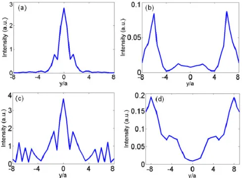
The transmission ratio between the middle points of the input and the output of the waveguide is calculated and compared with the numerical results. When we compare Figs. 7(a) and 7(b) with Figs. 8(a) and 8(b) it is noticed that there is a close agreement between the experimental and numerical results for linearly chirped waveguide structure. For the parabolically chirped waveguide case (comparing Figs. 7(c) and 7(d) with Figs. 8(c) and 8(d)), the strong field appearance in the central lobe for one direction and double-side lobes for the reverse direction appear with the experimental result as well. However, the central lobe is broader and the peaks of side lobes occur at a further away position. The asymmetric transmissions in addition to high-transmission contrast are obtained with microwave experiment. The non-smooth lines of experimental curves are due to a limited spatial scan of the detector antenna. Much smoother curves can be obtained by reducing the step size of scan along the y-direction.
Although the general characteristics of the operating frequencies match with the numerical study, the transmission ratios are lower in the measurements. The possible cause for the difference in the transmission ratios can be listed as the power loss in the z-direction and the inconsistencies in the calibration process of the antennas. The contrast rates of the opposite sites transmissions are measured as 24.8 dB and 30.8 dB for the linear and parabolic designs, respectively. As a conclusion, asymmetric power collection at the front end and the back end of the proposed structure can be seen in the experiments in agreement with the numerical results.
Fig. 7. The simulated intensity distributions are provided at the outside of the structure for microwave region. (a) The transverse field profile across the end face of the linearly chirped waveguide. (b) The transverse field profile across the front face of the same structure. (c) The transverse field profile across the end face of the parabolically chirped waveguide. (d) The transverse field profile across the front face of the same structure.
Fig. 8. The measured intensity distributions are provided at the outside of the structure. (a) The transverse field profile across the end face of the linearly chirped waveguide. (b) The transverse field profile across the front face of the same structure. (c) The transverse field profile across the end face of the parabolically chirped waveguide. (d) The transverse field profile across the front face of the same structure.
5. Additional Remarks
We should point out that the numerical calculation employed in the present work is based on two-dimensional analysis. Since the experiment was performed in the microwave region, one can take relatively long dielectric rods that are uniform along the out-of-plane direction (the height is many times larger than the operating wavelength). As a result, ideal two-dimensional assumption can be satisfied. 3D analysis assures the incorporation of the of-plane loss. As long as chirped PCW is not long which is indeed the case in our work, the out-of-plane loss is expected to be small. When we implement 3D analysis instead of 2D one, the available frequencies that provide strong asymmetric wave propagation will change (frequencies will move to higher values).
The first attempt of the study targets a device that can be operated at telecom wavelengths. Hence, we take the refractive index value of Silicon to be 3.46. Therefore, in the first part of the work, we assume 3.46 as a refractive index of the material. In Section IV, we implemented an experimental study and the available dielectric rods have refractive index of 3.1. As a result, we have additionally performed theoretical work with a refractive index 3.1 to determine the new frequency that yields asymmetric transmission and then made comparison with experimental results.
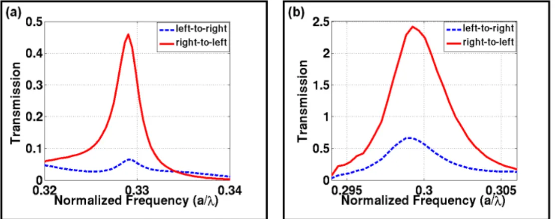
Fig. 9. Non-normalized transmission spectra for (a) linearly chirped photonic crystals and (b) quadratically chirped photonic crystals are shown for a refractive index of 3.46.
We have provided the contrast ratio graphs in Figs. 3(b) and 4(b). It would also be insightful to present transmission spectra. We have prepared the non-normalized transmission spectra of the oppositely propagating waves in Fig. 9. Due to the limited width of the chirped PCW, some part of light leaks at the transverse to propagation direction as can be seen in Figs. 3 and 4. As a result, the normalization process may become problematic. Therefore, non-normalized transmission spectra for linearly and quadratically chirped PCWs are shown in Figs. 9(a) and 9(b), respectively. By comparing the transmission spectra of waves propagating along the opposite directions, we can see that right-to-left propagation is moderately larger than the left-to-right propagation. The implementation of the two different chirping provides very similar contrast ratio. However, quadratically chirped PCW enable larger amount of light to be transported compared to linearly chirped PCW. The sole aim of presenting a second design based on parabolic chirping is to enhance the contrast ratio and transmission efficiency. As we have stated in Section 4, the contrast rates of the opposite sites transmission are ~25 dB and ~31 dB for linear and parabolic chirping, respectively (~6 dB improvement can be achieved by means of parabolic chirped PCW). Transmission efficiency of right-to-left direction is also higher in parabolic chirped PCW than linearly chirped PCW.
Figures 3 and 4 are collective results of linearly and parabolically chirped PCWs that are designed to provide asymmetric light propagation. The material refractive index is taken to be 3.46 due to the targeting telecom wavelengths and we have only theoretical results. On the
other hand, Figs. 7 and 8 demonstrate numerical and experimental results of linearly and parabolically chirped waveguides that are designed to operate at the microwave frequencies.
6. Conclusions
In conclusion, the aim of this work was to obtain an optical diode-like acting structure by utilizing chirped photonic crystals. For this goal, the distances between each neighboring column of rods of square lattice photonic crystal are modified to obtain a chirped device. The standard waveguide shows no diode like behavior due to the symmetry of the structure. Optical pulse propagates identically in either direction in a standard waveguide. Nonetheless, in the proposed waveguide designs, the propagation and transmission of light collected at the center of the structure are not the same in the two opposite directions. We witness the transmission asymmetry in the light propagation though the chirped PCW. The experimental results obtained at the microwave frequencies confirm the numerically observed asymmetric light propagation. The presented design based on the linear optic concept is a practical choice and may help the advancement of research activities utilizing the asymmetric light propagation of light. The ultimate engineering of chirping parameters not only in terms of lattice spacing but also using other parameters such as rods’ radii and refractive index parameters may give rise to the superior performance of the optical diode-like photonic structures.
Acknowledgments
This work is supported by the European Union (EU) under the projects PHOME, ECONAM, and N4E; by The Scientific and Technological Research Council of Turkey (TUBITAK) under the projects 110T306, 109E301, 107A004, and 107A012; and the State Planning Organization (DPT) under the project DPT-HAMIT. H. Kurt acknowledges support from the Turkish Academy of Sciences Distinguished Young Scientist Award (TUBA-GEBIP). One of the authors (E. Ozbay) also acknowledges partial support from the Turkish Academy of Sciences. D. Yilmaz and A. E. Akosman gratefully acknowledge financial support from TUBITAK-BIDEB.