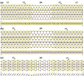
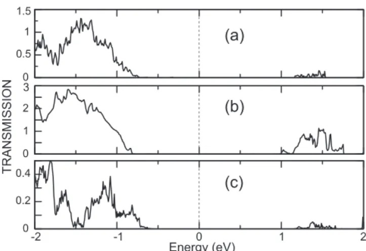
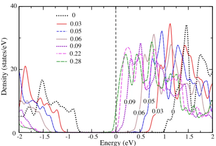
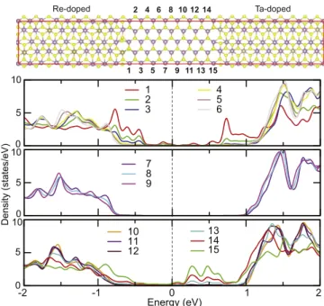
In pursuit of barrierless transition metal dichalcogenides lateral heterojunctions
Tam metin
Şekil
Benzer Belgeler
Zaviye, tekke ve dergâh gibi isimler altında ifade edilen bu mekânlar birbirinden hemen hemen farksız olan müesseselerdir.. Sadece büyüklükleri açısından
(&ate, “The hybrid AFM I STM lithography system,” unpublished. Colton, “Lithographic studies of an e-beam resist in a vacuum scanning tunneling microscope,”
The ethyl groups which protrude from the plane of the carbazole groups and the alkylene chain connecting the two carbazole groups are responsible for the poor molecular
The axial view of chest computed tomography (CT) scan revealed continuity of the line of the right lateral process of the second thoracic vertebra to the mass no other
Şekil 4.10’da verilen dış hava sıcaklığına bağlı soğutma gruplarının toplam tüketimi grafiğinde regresyon katsayısı 0.7755 olarak bulunmuş, katsayının
Ölmüş, kendini savunamaz duruma gelmiş bir büyük ya zarı, bir kahramanı anlatırken yapıtlarından giderek anlatma lı, yani ürünleriyle ele almalı,
「100 年全國大專校院績優學生社團評鑑」,空前雙料冠軍! 本校服務性社團「杏青康輔社服團」及學術學藝性社團「中國醫藥研習社」,於 3
The main goal of this paper was analyzing the cloud computing security threats, attacks and the data protection techniques in the cloud computing which defined the
