36
1 QELS'96
TUESDAY MORNINGfor publication in J. Vac. Sci. Tech- nol. (Dec. 1995).
6. G.
Z.
Qian and K. M. Leung, Phys. Rev. B 44, 11482 (1991).QTuA7 9:45 am
Resonant cavity-enhanced detectors embedded in photonic crystals
B.
Temelkuran, E. Ozbay, Department of Physics, Bilkent University, Bilkent Ankara 06533 ZbrkeyThere is a great deal of current interest in the possibility of creating three-dimen- sional photonic band crystals in which no electromagnetic (EM) propagation is pos- sible for certain frequenaes.' Recently, Ho et al. have proposed a new photonic crystal based on stacked dielectric rods (Fig. l), which can be fabricated at smaller scales by conventional methods? Defects or cavities around the same ge- ometry can also be built by addition of removal of rods from the crystals? The electrical fields in such cavities are usu- ally enhanced, and by placing active de- vices in such cavities one can obtain novel properties. This effect has been used already in optoelectronics to achieve novel devices such as resonant-cavity-en- hanced (RCE) photodetectors and light- emitting diodes.' In this paper, we dem- onstrate the RCE effect by placing microwave detectors in a layer-by-layer photonic crystal.
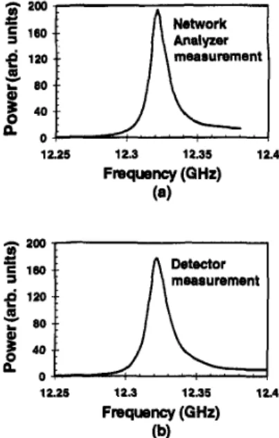
We used the output of a network an- alyzer as the microwave source, and fed the output to a hom antenna to obtain EM waves. The crystal was then replaced in the beam-path of the EM wave, and the electric field inside the cavity was measured by a probe that consisted of a monopole antenna. The output of the an- tenna was measured by use of two dif- ferent techniques: network analyzer and microwave detector within the cavity.
The first cavity structure was similar to a one-dimensional Id Fabry-Perot res- onator made of two mirrors separated by a distance. The front mirror structure was six layers thick, and the back mirror was eight layers thick, with a 7-mm separa- tion between the two mirrors. Both tech- niques have shown a typical power en- hancement factor of 180, with a quality factor of 1200 (Fig. 2). The agreement be- tween two measurements also showed the reliability of the microwave detector. To obtain a localized defect, we mod-
X
QTuA7 Fig. 1 Schematic of the layer- by-layer photonic crystal.
3
2oo5
1809
120 Jz
P o 40 measurementK
12.25 12.3 12.35 12.4 Frequency (QHz)(4
Detector measurement 80 40 0 1226 12.3 12.35 12A Frequency (GHz) (b)QTuA7 Fig. 2 Measured power of the EM field inside a one-dimensional defect structure with use of (a) network analyzer or @) microwave detector.
Detector Measurement
0
12.3 12.32 12.34 12.30 12.30 12.4
Frequency (GHz) QTuA7 Fig. 3 Measured power of the EM field inside a localized defect structure with use of a microwave detector.
ified a 16-layer crystal structure in the fol- lowing manner. Parts of the rods on the 8th and 9th layer were removed such that we obtained a rectangular prism-like cav- ity. The dimensions of the cavity were h
X h X 2d, where a is the center-to-center distance between parallel rods and d is the thickness of the alumina rods. A mi- crowave detector was placed in the pho- tonic crystal, and a monopole antenna was connected to the input of the detec- tor. The hybrid antenna-detector was then used to probe the EM field inside the localized cavity Figure 3 shows the measured magnitude of the EM field with the detector. A power enhancement factor of 35 was measured for this cavity, which clearly indicates the resonant cav- ity enhancement for a localized defect.
Our results suggest the possibility of use of the embedded detector as an RCE detector. By use of a smaller size photonic crystal and a higher-frequency detector, the effect can also be shown at millimeter and far-infrared frequencies. Such RCE detectors will have increased sensitivity
and efficiency when compared with con- ventional detectors and can be used for various applications where sensitivity and efficiency are important parameters. 1. E. Yablonovitch et al., Phys. Rev.
Lett. 63, 1950 (1989). 2.
K.
M. Ho et al., Solid State CO".89, 413 (1994).
3.
E.
Ozbay et al., Phys. Rev. B 51, 13961 (1995).4. M. S. Unlu et al., J . Appl. Phys. 78,
R1-R33 (1995).
JTuB
8:30 am
Salon F
Joint Symposium on Quasi-Phase
Matching
Nasser Peyghambarian, University of Arizona, Presider
JTuBl (Tutorial) 8:30 am Microstructured media for nonlinear optics: Materials, devices, and applications M. M. Fejer, E.
L.
Ginzton Laboratory, Stanford, California 94305The past decade has seen a renaissance in coherent sources based on nonlinear optical frequency conversion, fueled by improved pump lasers and improve- ments in available nonlinear materials. Microstructured nonlinear materials, es- pecially those in which the nonlinear sus- ceptibility is periodically reversed to quasi-phasematch (QPM) the nonlinear interaction, are playing an increasingly important part in these developments. Application of periodically poled ferro- electrics, the most important class of QPM materials, has allowed qualitative improvements in coherent sources from the ultraviolet to the mid-infrared. The increase in conversion efficiency avail- able with these materials also enables ef- fective application of quadratic nonlinear optics beyond simple sources of coherent radiation, in fields such as quantum op- tics, wavelength conversion for WDM systems, and cascade nonlinearities. By shifting the emphasis from materials with appropriate birefringence to those with pattemable nonlinear properties, the use of QPM opens opportunities to take advantage of the attractive proper- ties of materials not traditionally used in frequency conversion applications, such as cubic 111-V and 11-VI semiconductors, polymers, and glasses.
This tutorial will review basic ideas of QPM nonlinear optics, characteristics. of available microstructured media, and re- cent device results in QPM bulk and waveguide SHG, DFG, and OPOs. O p - portunities in novel microstructured ma- terials and in applications beyond sources of coherent radiation will also be discussed.