Contents lists available atScienceDirect
Physica B: Condensed Matter
journal homepage:www.elsevier.com/locate/physbThe effect of indium doping concentration on the electrical and dielectric
properties of Al/In:ZnO/p-Si heterojunctions
M. Yıldırım
a, M.O. Erdal
b, A. Kocyigit
c,*aSelcuk University, Faculty of Science, Department of Biotechnology, 42130, Konya, Turkey
bNecmettin Erbakan University, Meram Vocational School, 42090, Konya, Turkey
cIgdir University, Engineering Faculty, Department of Electrical and Electronics Engineering, 76000, Igdir, Turkey
A R T I C L E I N F O Keywords:
In doped ZnO thin film Interface states Impedance spectroscopy Frequency depending Dielectric properties Al/In:ZnO/p-Si heterojunction A B S T R A C T
Undoped and 0.1% 0.5% and 1.0% indium doped ZnO thin films were obtained by spin coating method as interfacial thin film layer between Al metal and p-Si semiconductor to investigate dielectric properties of the Al/ In:ZnO/p-Si heterojunctions. Impedance spectroscopy technique was employed to characterize the dielectric properties of the Al/In:ZnO/p-Si heterojunctions depending on frequency (from 10 kHz to 1 MHz) and voltage (from −5 V to +5 V). The results imparted that interface states (Nss), series resistance (Rs), barrier height ( b)
and the concentration of acceptor atoms (Na) influenced frequency changes. The dielectric parameters such as
dielectric constant ( ), dielectric loss ( ), loss tangent (tan δ), real and imaginary parts of the electric modulus (M and M ) and ac electrical conductivity (σ) values were calculated from impedance spectroscopy measure-ments and discussed in details for changing frequency and voltage for various In doped ZnO thin film interlayers. The dielectric properties of the Al/In:ZnO/p-Si heterojunctions were affected both In doping concentration and the frequency and voltage changes. The Al/In:ZnO/p-Si heterojunctions can be considered for industrial appli-cations to increase the control.
1. Introduction
Zinc oxide (ZnO) is a non-toxic, low-cost material, and has large exciton binding energy (60 meV), high dielectric constant and a wide band gap (3.37 eV) [1–3]. These properties can make ZnO a good candidate for interfacial layer to control the electrical properties of the semiconductor heterojunctions. In addition to these good properties, electrical conductivity of the ZnO can be controlled by a dopant ele-ment such as In, Fe, Al, etc [4–6]. When the ZnO doped with In, n-type ZnO is obtained according to the literature [7–9]. The undoped and doped ZnO can be employed as an interfacial layer in the metal-oxide-semiconductor (MOS) heterojunctions because of their promising properties [10–13]. The MOS heterojunctions have important applica-tions in the industry because they can be employed in rectifying, in-verting and diode applications [14–16]. The MOS structures have been investigated over many years via various interfacial layers [17–21]. These interfacial layers provide the heterojunctions with controlling their electrical properties [22,23].
The electrical characterization of MOS heterojunctions is really important to understand their application areas. Especially, dielectric characterization provides us the understanding of the conduction and
polarization mechanism [24]. The polarization mechanism can be ionic, electronic, surface polarization or dipolar polarizations according to the magnitude of the applied frequency [25]. At high or intermediate frequencies (103–106Hz), non-dipole polarization is occurred de-pending on relaxation time (τ). This case is attributed to impurities, surface charges and existence of constant orientable dipoles and is important for characterization of these heterojunctions [26]. Badali et al. [27] fabricated Au/ZnO/n-Si (MIS) structures by RF sputtering technique and investigated their dielectric properties by impedance spectroscopy technique from 0.7 kHz to 1 MHZ frequency range. They concluded that the Au/ZnO/n-Si structures have different conduction mechanism at low and higher frequencies. In addition, the dielectric properties changed as a function of frequency and voltage. Buyukbas-Ulusan et al. [28] obtained Al/CdxZn1−xO/p-Si heterostructures by spin coating technique for 10%, 20% and 30% Cd doped ZnO interfacial layers and characterized by admittance spectroscopy technique for −5 V and +5 V voltage range at 1 MHz frequency. They extracted main electrical parameters such as barrier height, depletion region width from admittance measurements. According to results, they ex-plained that the dielectric constant values increased with increasing Cd doping to ZnO interfacial layer. Orak et al. [24] fabricated Au/ZnO/n-Si
https://doi.org/10.1016/j.physb.2019.07.055
Received 2 July 2019; Received in revised form 30 July 2019; Accepted 31 July 2019
*Corresponding author. Igdir University, Engineering Faculty, Department of Electrical and Electronics Engineering, 76000, Igdir, Turkey.
E-mail addresses:[email protected],[email protected](A. Kocyigit).
Available online 01 August 2019
0921-4526/ © 2019 Elsevier B.V. All rights reserved.
device by atomic layer deposition and studied electrical and dielectric properties by impedance spectroscopy. They concluded that interface charges and polarization were more effective at lower frequencies.
There are many studies about ZnO based dielectric materials in the literature but there are no studies about In doped ZnO interfacial layer for dielectric properties according to our best knowledge [3,24,25,29]. In this study, undoped and various In doped ZnO interfacial layers were grown on p-type Si wafer as oxide layer, and the Al/In:ZnO/p-Si het-erojunctions were fabricated and characterized by impedance spectro-scopy technique to investigate their electrical and dielectric properties for various frequencies.
2. Experimental details
Zinc acetate dehydrate (Zn(CH3COO)2·2H2O) was solved in iso-propanol as precursors, and indium nitrate hydrate (In(NO3)3·H2O) was dissolved in metoxyethanol to achieve 0.1%, 0.5% and 1.0% In doped ZnO thin films in different vessels. The ethanolamine was included as the stabilizer for both the precursor and doping solutions. The precursor and various In doping solutions were mixed and stirred 1 h to obtain In doped ZnO thin films solutions. Meanwhile, a p-type Si wafer, which had 7.3 × 1015cm−3carrier concentrations, was cut to 1 cm2pieces. They were cleaned in an ultrasonic cleaner by acetone and propanol, and dumped into HF:H2O (1:1) solution for 30 s to remove the native oxide layer and impurities from the surfaces. An aluminum (Al) layer (100 nm) was vaporized to the back surface of the wafer pieces by a thermal evaporator. The Al vaporized pieces were tempered in N2 medium for 5 min at 500 °C to achieve ohmic contacts. The prepared undoped and various In doped ZnO thin films solutions were deposited on the front surface of p-type Si wafer pieces by a spin coater at 3000 rpm as three layers. Thus, the undoped and various In doped ZnO interfacial layers were acquired on the p-type Si wafer pieces. Then, another Al layer was evaporated to the In doped ZnO film surfaces as 100 nm thicknesses by thermal evaporator as rectifying contact via hole array mask. The schematic illustration of the obtained heterojunctions has been shown inFig. 1. Here, there are two regions which are cor-responding to the p/n and metal/semiconductor (M/S) junction. How-ever, the n-type ZnO layer is not a very good crystal as like p-type Si and can be thought as dielectric material between the metal and semi-conductor to control the electric properties of the heterojunctions.
The film thicknesses of the undoped and various In doped ZnO films were determined by Veeco Dektak 150 profilometer. The film thick-nesses of the undoped and 0.1%, 0.5% and 1.0% In doped ZnO thin films are 208 nm, 212 nm, 202 nm and 213 nm, respectively according to profilometer measurements. The fabricated heterojunctions were characterized by impedance spectroscopy measurements. A Keithley 4200 semiconductor characterization system (SCS) were employed for impedance spectroscopy measurements for 10 kHz and 1 MHz fre-quency range from −5 V to +5 V biases.
3. Results and discussion
The obtained various In doped heterojunctions were characterized by impedance spectroscopy technique to understand the heterojunction characteristics such as series resistance (Rs), interface state density (Nss) and dielectric parameters. The NssandRsinfluence electrical properties of the heterojunction and should be studied to determine the conduc-tion mechanism of these kinds of heterojuncconduc-tions [30,31]. It should be noted that the Nss originates from trapped charges, moving ions and stable oxide ions in the heterojunctions, and theRsis caused by ohmic or rectifier contacts, non-uniform film structures and resistance of the semiconductor or interlayer film in the heterojunction [32].
The relation between the Nss and frequency is obtained by Hill-Coleman technique. The Nssis given by the next equation according to this technique: = + N qA G G C C C 2 ( / ) (( / ) / ) (1 / ) ss m max m max 0x2 m 0x2 (1)
where, A and ( 2 )= f represent rectifier contact area and angular frequency, the G( m/ )max andCm are the measured conductance and capacitance, respectively. TheC0x shows interfacial insulator or oxide layer capacitance for strong accumulation region. It is expressed by the following relation: = + C C G C [1 ( ) ] x ma ma ma 0 2 2 (2)
Nicollian and Brews method helps to determine frequency depen-dentRs values from the measured conductance and capacitance [31]. TheRsis shown by the next equation according to this technique:
= + R G G ( C ) s ma ma2 ma2 (3)
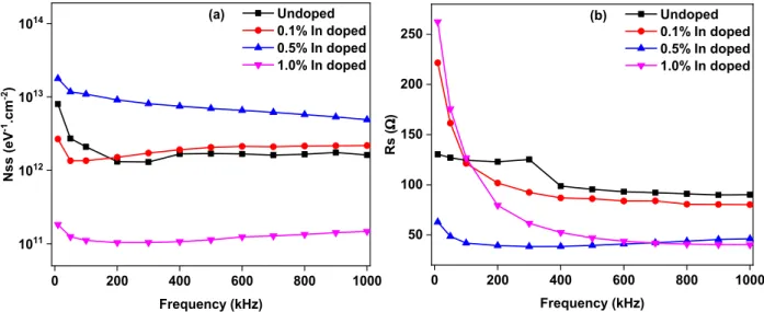
whereGmaandCmaare showing the conductance and capacitance values for strong accumulation region, respectively.Fig. 2a and b shows fre-quency dependent profile of the Nss andRsfor various In doped Al/ In:ZnO/p-Si heterojunctions. According toFig. 2a and b, the NssandRs values decreased with increasing frequency and stayed constant up to higher frequencies. While the minimum Nssvalues were obtained via 1.0% In doping to the ZnO film structure, the maximum values were measured for 0.5% In doping level. The highest Nssvalues for 0.5% In doped Al/In:ZnO/p-Si heterojunction highlighted that this heterojunc-tion had more defects than others or more charge carriers [33]. Fur-thermore, the results highlighted that theRsvalues were not effective towards to higher frequencies depending on the Nss[34]. The obtained
NssandRs values for various In doped Al/In:ZnO/p-Si heterojunction are suitable for electronic devices.
The barrier height ( b) and concentration of acceptor atoms (Na) are other important parameters for the characterization MOS heterojunc-tions. The b values are calculated by below equation depending on Fermi energy level (EF) and diffusion potential (Vd):
= +
C V V E
( ) ( )
b d F (4)
where is the image force barrier lowering (can be neglected for low frequencies).Fig. 3a and b indicate frequency dependent changing of
Na and b values for Al/In:ZnO/p-Si heterojunctions. The Na values decreased at lower frequencies and then remained almost constant for higher frequencies according toFig. 3a. This case can be attributed to undoped and In doped ZnO interfacial layer and the particular dis-tribution of Nss[35]. Furthermore, while 0.5% In doped Al/In:ZnO/p-Si heterojunction highestNavalues, the 1.0% In doped heterojunction has the lowestNavalues. This result approves that various In doping levels have been achieved and more acceptor atom contributions have been gained by In doping to the ZnO structures. Normally, the p-Si has 7.3 × 1015cm−3carrier concentrations or acceptor atoms according to manufacturer. However, the calculatedNavalues are higher than p-Si. This is the proof of the In doping to the ZnO lattice. According to
Fig. 3b, the bvalues have fluctuation for undoped and 0.5% In doped heterojunctions. However, the bvalues usually decreased for undoped, 0.1%, and 1.0% In doped heterojunctions for lower frequencies and remained stable for higher frequencies. In the case of 0.5% In doped heterojunction, the bvalues increased with increasing frequency. The increasing bvalues can be attributed to the existence of more defects in the interface of the heterojunction. When the obtained Naand b values are compared via Al/p-Si heterojunction in the literature, theNa values are changed in the range of 1014-1016cm−1and the
b values are around 1.0 eV smaller than this study [36–38]. The higher values of theNaand bvalues can be attributed to In doped ZnO layers between the Al and p-Si. Moreover, the coverage of the ZnO thin films is not uniform all over the substrate depending on the thin film technique according to our previous work [13]. This can be affect barrier height values of the heterojunctions due to barrier inhomogeneities.
To obtain more information about conduction and polarization mechanisms, complex dielectric permittivity ( =* j ) is studied for wide range frequency and voltage. While the real dielectric constant represents the stored energy and the strength of the dipole against applied electric field, imaginary dielectric constant exhibits consumed energy owing to frictional dampening [39].
The complex permittivity is expressed via following formula with its components: = j = C C j G C * 0 0 (5)
where and indicate real and imaginary components of ε*, respec-tively. While the G and C are the measured conductance and capaci-tance, the C0and j are capacitance of free capacitor and imaginary root, respectively. If the values of and are expressed according to the free capacitor formula, next equations are obtained [26]:
= C = C Cd A i 0 0 (6) = G = C Gd A i 0 0 (7)
where diand 0are interlayer thickness and vacuum permittivity. The
maximum capacitance value for accumulation region is related to the interlayer capacitance and addressed asCac=Ci= 0A d/ i. The loss tangent (tan δ) is given by below equation:
= = G
C
tan (8)
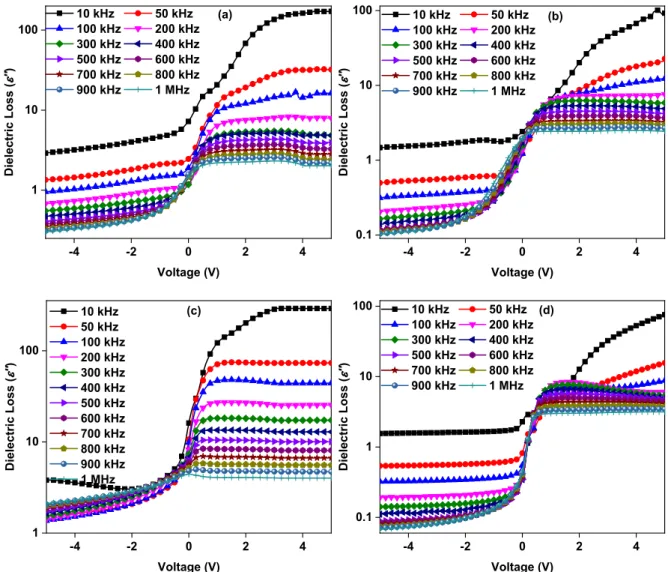
The dielectric constant versus voltage graphs of the Al/In:ZnO/p-Si heterojunctions have been shown inFig. 4a–d for undoped, 0.1%, 0.5% and 1.0% In doped, respectively for 10 kHz and 1 MHz frequency range. The values almost did not change in inversion region but increased
0 200 400 600 800 1000 1011 1012 1013 1014 (a) N ss (eV -1.c m -2) Frequency (kHz) Undoped 0.1% In doped 0.5% In doped 1.0% In doped 0 200 400 600 800 1000 50 100 150 200 250 (b) R s ( ) Frequency (kHz) Undoped 0.1% In doped 0.5% In doped 1.0% In doped
Fig. 2. (a) The Nssand (b) Rsversus frequency plots of the Al/In:ZnO/p-Si heterojunctions.
0 200 400 600 800 1000 1016 1017 1018 1019 (a) N a (c m -3) Frequency (kHz) Undoped 0.1% In doped 0.5% In doped 1.0% In doped 0 200 400 600 800 1000 1 2 3 4 5 6 (b) B ar rie rH eig ht ( eV
)
) Frequency (kHz) Undoped 0.1% In doped 0.5% In doped 1.0% In dopedquickly in the depletion region and then exhibited peaks in the accu-mulation region. The peak positions of altered towards to the de-pletion region. The peak intensities of decreased via increasing fre-quency because the Nss cannot follow ac signal at higher frequencies [40]. Furthermore, the varying at the values are depended to the Maxwell-Wagner interfacial polarization because of accumulating the charge carriers at the boundaries and causing interfacial polarization [41]. Moreover, the heterojunctions demonstrated negative dielectric constant values for higher frequencies and forward biases. The negative values can be based on the extinction of the interfacial charges lo-calized at the interface of the metal-semiconductor [42]. The ZnO has a dielectric constant in the range of 2–40 according to the literature [43,44], but in this study the determined dielectric values reached to 140 for 0.5%. This higher dielectric constant may be caused defect ef-fects due to non-homogenous doping.
Fig. 5a–d display the dielectric loss versus voltage plots of the un-doped, 0.1%, 0.5% and 1.0% In doped Al/In:ZnO/p-Si heterojunctions for various frequencies, respectively. In the inversion region, the values slightly decreased with increasing frequency but increased by increasing voltage for almost all heterojunctions. However, the va-lues were strongly affected at depletion and accumulation regions from the frequency and voltage changes. At these regions, the charge carriers caused the loss of the energy owing to increasing speed of the charge recombination. Furthermore, the values decreased with increasing frequency at accumulation region because of not to following ac signal
at higher frequencies [45]. The highest loss values have been obtained for 0.5% In doped Al/In:ZnO/p-Si heterojunction due to having most defects between the obtained heterojunctions.
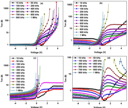
Fig. 6a–d indicate tan δ versus voltage graphs of the various In doped Au/In:ZnO/p-Si heterojunctions for changing frequencies. The tan δ values decreased slightly in the inversion region with increasing frequency (except 0.5% In doping heterojunction), but increased and exhibited peaks at the depletion and accumulation regions. The tan δ values changed strongly in the depletion and accumulation regions depending on the frequency and voltage due to the increasing charges carriers with changing biases from reverse to forward biases.
The complex dielectric constant can provide complex electric modulus with calculating owing to the relation of ε* = 1/M*. Complex electric modulus is expressed asM*=M +jM formalism and helps understand the relaxation process of a dielectric material [42]. Real and imaginary parts of the electric modulus given by the next equation with dependent on the and values [26]:
= =
+ + + = +
M* 1 j M jM
* 2 2 2 2 (9)
Fig. 7a–d exhibit M versus voltage graphs of the various In doped Al/In:ZnO/p-Si heterojunctions for increasing frequency from 10 kHz to 1 MHz. While the M values increased with increasing frequency in inversion and depletion regions owing to the relaxation of the polar-ization, they became independent of frequency and voltage changes at
-4 -2 0 2 4 -5 0 5 10 15 20 25 (a) D ie le ct ric C on st an t( ') Voltage (V) 10 kHz 50 kHz 100 kHz 200 kHz 300 kHz 400 kHz 500 kHz 600 kHz 700 kHz 800 kHz 900 kHz 1 MHz -2 -1 0 1 2 3 4 5 0 1 2 Voltage (V) -4 -2 0 2 4 0 2 4 6 8 10 12 14 16 (b) D ie le ct ric C on st an t( ') Voltage (V) 10 kHz 50 kHz 100 kHz 200 kHz 300 kHz 400 kHz 500 kHz 600 kHz 700 kHz 800 kHz 900 kHz 1 MHz -4 -2 0 2 4 0 20 40 60 80 100 120 140 (c) D ielec tr ic C on st an t( ') Voltage (V) 10 kHz 50 kHz 100 kHz 200 kHz 300 kHz 400 kHz 500 kHz 600 kHz 700 kHz 800 kHz 900 kHz 1 MHz -4 -2 0 2 4 0 3 6 9 12 15 (d) D ie lec tr ic C on st an t( ') Voltage (V) 10 kHz 50 kHz 100 kHz 200 kHz 300 kHz 400 kHz 500 kHz 600 kHz 700 kHz 800 kHz 900 kHz 1 MHz
accumulation regions except 0.5% In doped Al/In:ZnO/p-Si hetero-junction [14]. It is believed that the more defects at the interface of Al/ In:ZnO/p-Si heterojunctions caused changes of relaxation mechanism and polarization process differently.
Fig. 8a–d show the M -V plots of the various In doped Al/In:ZnO/p-Si heterojunctions for changing frequency. The M values increased via increasing frequency up to 200 kHz and then decreased in the inversion region for 0.1% and 1.0% In doped Al/In:ZnO/p-Si heterojunctions. However, in the case of undoped and 0.5% In doped heterojunctions, the M values increased with increasing frequency in the inversion, depletion and accumulation regions. Furthermore, the M values de-creased from the inversion to depletion regions and remained constant in the accumulation regions for all devices via changing voltage. Such kind of changes at the M values approve the relaxation time of the charges and their particular distribution at surface states [46].
The ac electric conductivity ( ) is calculated via the following equation depending on imaginary dielectric constant:
= d =
A C
( ) tan 0 (10)
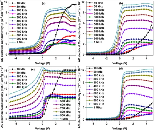
The versus voltage plots of the various In doped Al/In:ZnO/p-Si heterojunctions have been displayed in Fig. 9a–d for increasing fre-quency from 10 kHz to 1 MHz. While the values increased greatly for 0.5% In doped Al/In:ZnO/p-Si heterojunction, they slightly increased at inversion regions via increasing frequency for undoped, 0.1%, and 1.0% In doped Al/In:ZnO/p-Si heterojunctions. This difference can be at-tributed to the existence of more charge carriers and defects at the
interface of the 0.5% In doped Al/In:ZnO/p-Si heterojunction. Fur-thermore, the values stayed constant in the inversion and accumu-lation regions but increased suddenly in the depletion region for all heterojunctions for higher frequencies than 50 kHz. The increase at values via increasing frequency can be attributed to the increasing eddy current and decreasing series resistance of the heterojunction [47,48]. 4. Conclusion
The undoped, 0.1%, 0.5% and 1.0% In doped ZnO thin film were synthesized on p-type Si substrate by spin coating technique and in-serted as interfacial thin films layers between the Al and p-Si to fabri-cate various In doped Al/In:ZnO/p-Si heterojunctions. Their electrical and dielectric properties were investigated by impedance spectroscopy technique depending on frequency and voltage. The profile of the Nss andRswith changing frequency revealed that the NssandRsdecreased with increasing frequency. In addition, theNaand bvalues decreased at lower frequencies and then remained constant up to higher fre-quencies. While the and values decreased with increasing fre-quency, the tan δ values usually increased. The , and tan δ values exhibited peaks at low accumulation region. The values of M are ef-fective in the inversion region with increasing frequency, but the M values are effective in the inversion, depletion and accumulation re-gions. The values increased with increasing frequency in the deple-tion and accumuladeple-tion regions. According to results, the dielectric parameters are strongly depended on frequency and voltage. The Al/
-4 -2 0 2 4 1 10 100 (a) D ie le ct ric Lo ss ( '') Voltage (V) 10 kHz 50 kHz 100 kHz 200 kHz 300 kHz 400 kHz 500 kHz 600 kHz 700 kHz 800 kHz 900 kHz 1 MHz -4 -2 0 2 4 0.1 1 10 100 (b) D ie le ct ric Lo ss ( '') Voltage (V) 10 kHz 50 kHz 100 kHz 200 kHz 300 kHz 400 kHz 500 kHz 600 kHz 700 kHz 800 kHz 900 kHz 1 MHz -4 -2 0 2 4 1 10 100 (c) D ie le ct ric Lo ss ( '') Voltage (V) 10 kHz 50 kHz 100 kHz 200 kHz 300 kHz 400 kHz 500 kHz 600 kHz 700 kHz 800 kHz 900 kHz 1 MHz -4 -2 0 2 4 0.1 1 10 100 (d) D ie le ct ric Lo ss ( '') Voltage (V) 10 kHz 50 kHz 100 kHz 200 kHz 300 kHz 400 kHz 500 kHz 600 kHz 700 kHz 800 kHz 900 kHz 1 MHz
-4 -2 0 2 4 1 10 100 1000 (a) Tan ( ) Voltage (V) 10 kHz 50 kHz 100 kHz 200 kHz 300 kHz 400 kHz 500 kHz 600 kHz 700 kHz 800 kHz 900 kHz 1 MHz -4 -2 0 2 4 1 10 100 1000 (b) Tan ( ) Voltage (V) 10 kHz 50 kHz 100 kHz 200 kHz 300 kHz 400 kHz 500 kHz 600 kHz 700 kHz 800 kHz 900 kHz 1 MHz -4 -2 0 2 4 1 10 100 1000 (c) Ta n ( ) Voltage (V) 10 kHz 50 kHz 100 kHz 200 kHz 300 kHz 400 kHz 500 kHz 600 kHz 700 kHz 800 kHz 900 kHz 1 MHz -4 -2 0 2 4 1 10 100 (d) Ta n ( ) Voltage (V) 10 kHz 50 kHz 100 kHz 200 kHz 300 kHz 400 kHz 500 kHz 600 kHz 700 kHz 800 kHz 900 kHz 1 MHz
Fig. 6. The loss tangent versus voltage plots of the a) undoped, b) 0.1%, c) 0.5% and d) 1.0% In doped Al/In:ZnO/p-Si heterojunctions.
-4 -2 0 2 4 0.0 0.2 0.4 0.6 0.8 1.0 1.2 1.4 1.6 R eal Ele ct ric Mo du lu s (M' ) Voltage (V) 10 kHz 50 kHz 100 kHz 200 kHz 300 kHz 400 kHz 500 kHz 600 kHz 700 kHz 800 kHz 900 kHz 1 MHz (a) -4 -2 0 2 4 0 1 2 3 (b) R ea lE lec tr ic Mo du lu s (M' ) Voltage (V) 10 kHz 50 kHz 100 kHz 200 kHz 300 kHz 400 kHz 500 kHz 600 kHz 700 kHz 800 kHz 900 kHz 1 MHz -4 -2 0 2 4 -0.1 0.0 0.1 0.2 (c) R eal Ele ct ric Mo du lu s (M' ) Voltage (V) 10 kHz 50 kHz 100 kHz 200 kHz 300 kHz 400 kHz 500 kHz 600 kHz 700 kHz 800 kHz 900 kHz 1 MHz -4 -2 0 2 4 0 1 2 3 4 (d) R ea lE le ct ric Mo du lu s (M' ) Voltage (V) 10 kHz 50 kHz 100 kHz 200 kHz 300 kHz 400 kHz 500 kHz 600 kHz 700 kHz 800 kHz 900 kHz 1 MHz
-4 -2 0 2 4 0.0 0.2 0.4 0.6 0.8 1.0 1.2 1.4 1.6 (a) Im ag in ar y Ele ct ric Mo du lu s (M' ') Voltage (V) 10 kHz 50 kHz 100 kHz 200 kHz 300 kHz 400 kHz 500 kHz 600 kHz 700 kHz 800 kHz 900 kHz 1 MHz -4 -2 0 2 4 0.0 0.2 0.4 0.6 0.8 1.0 1.2 1.4 1.6 (b) Im ag in ar y Ele ct ric Mo du lu s (M' ') Voltage (V) 10 kHz 50 kHz 100 kHz 200 kHz 300 kHz 400 kHz 500 kHz 600 kHz 700 kHz 800 kHz 900 kHz 1 MHz -4 -2 0 2 4 0.00 0.05 0.10 0.15 0.20 0.25 0.30 (c) Im ag in ar y Ele ct ric Mo du lu s (M' ') Voltage (V) 10 kHz 50 kHz 100 kHz 200 kHz 300 kHz 400 kHz 500 kHz 600 kHz 700 kHz 800 kHz 900 kHz 1 MHz -4 -2 0 2 4 0.0 0.5 1.0 1.5 2.0 (d) Im ag in ar y Elec tr ic Mo du lu s (M' ') Voltage (V) 10 kHz 50 kHz 100 kHz 200 kHz 300 kHz 400 kHz 500 kHz 600 kHz 700 kHz 800 kHz 900 kHz 1 MHz
Fig. 8. The imaginary part of dielectric modulus versus voltage plots of the a) undoped, b) 0.1%, c) 0.5% and d) 1.0% In doped Al/In:ZnO/p-Si heterojunctions.
In:ZnO/p-Si heterojunctions can be employed for industrial applica-tions.
Conflict of interest
All authors declare that there is no conflict of the interest. References
[1] S. Banu, S.J. Ahn, S.K. Ahn, K. Yoon, A. Cho, Fabrication and characterization of cost-efficient CuSbS2 thin film solar cells using hybrid inks, Sol. Energy Mater. Sol. Cells 151 (2016) 14–23.
[2] I. Orak, A. Kocyigit, A. Turut, The surface morphology properties and respond il-lumination impact of ZnO/n-Si photodiode by prepared atomic layer deposition technique, J. Alloy. Comp. 691 (2017) 873–879.
[3] A.-S. Gadallah, M.M. El-Nahass, Structural, optical constants and photo-luminescence of ZnO thin films grown by sol-gel spin coating, Adv. Condens. Matter Phys. 2013 (2013) 1–11.
[4] J. Ghosh, R. Ghosh, P.K. Giri, Tuning the visible photoluminescence in Al doped ZnO thin film and its application in label-free glucose detection, Sens. Actuators B Chem. 254 (2018) 681–689.
[5] T. Srinivasulu, K. Saritha, K.T.R. Reddy, Synthesis and characterization of Fe-doped ZnO thin films deposited by chemical spray pyrolysis, Mod. Electron. Mater. 3 (2) (2017) 76–85.
[6] M.S. Kim, K.G. Yim, S. Kim, G. Nam, D. Lee, J. Soo, J. Su, Growth and character-ization of indium-doped zinc oxide thin films prepared by sol – gel method, Acta Phys. Pol. A 121 (1) (2012) 3–6.
[7] S. Ilican, M. Caglar, Y. Caglar, Determination of the thickness and optical constants of transparent indium-doped ZnO thin films by the envelope method, Mater. Sci. 25 (3) (2007) 709–718.
[8] E.F. Keskenler, G. Turgut, S. Doğan, Investigation of structural and optical prop-erties of ZnO films co-doped with fluorine and indium, Superlattice Microstruct. 52 (1) (2012) 107–115.
[9] H.E. Silva-Lopez, B.S. Marcelino, A. Guillen-Cervantes, O. Zelaya-Angel, R. Ramirez-Bon, H.E. Silva-Lopez, B.S. Marcelino, A. Guillen-Cervantes, O. Zelaya-Angel, R. Ramirez-Bon, Physical properties of sputtered indium-doped ZnO films deposited on flexible transparent substrates, Mater. Res. 21 (6) (2018). [10] A.B. Yadav, C. Periasamy, S. Bhaumik, S. Jit, Hydrogen gas sensing properties of
Pd/ZnO thin films grown on n-Si substrates at room-temperature by thermal eva-poration and sol-gel techniques: a comparative study, Indian J. Pure Appl. Phys. 51 (2013) 792–799.
[11] Y. Nam, I. Hwang, S. Oh, S. Lee, K. Lee, S. Hong, J. Kim, T. Choi, B. Ho Park, Switchable Schottky diode characteristics induced by electroforming process in Mn-doped ZnO thin films, Appl. Phys. Lett. 102 (16) (2013) 162105.
[12] S.O. Tan, H. Uslu Tecimer, O. Çiçek, H. Tecimer, İ. Orak, Ş. Altındal, Electrical characterizations of Au/ZnO/n-GaAs Schottky diodes under distinct illumination intensities, J. Mater. Sci. Mater. Electron. 27 (8) (2016) 8340–8347.
[13] M. Yıldırım, A. Kocyigit, Characterization of Al/In:ZnO/p-Si photodiodes for var-ious in doped level to ZnO interfacial layers, J. Alloy. Comp. 768 (2018) 1064–1075.
[14] A. Kaya, Ş. Altındal, Y.Ş. Asar, Z. Sönmez, On the voltage and frequency distribution of dielectric properties and ac electrical conductivity in Al/SiO 2/p-Si (MOS) ca-pacitors, Chin. Phys. Lett. 30 (1) (2013) 017301.
[15] A. Kumar, S. Mondal, S.G. Kumar, K.S.R. Koteswara Rao, High performance sol–gel spin-coated titanium dioxide dielectric based MOS structures, Mater. Sci. Semicond. Process. 40 (2015) 77–83.
[16] S. Kaya, E. Yilmaz, A comprehensive study on the frequency-dependent electrical characteristics of Sm2O3 MOS capacitors, IEEE Trans. Electron Devices 62 (3) (2015) 980–987.
[17] E.H. Nicollian, J.R. Brews, MOS (Metal Oxide Semiconductor) Physics and Technology, Wiley-Interscience, 1982 First.
[18] C. Lu, L. An, Q. Fu, J. Liu, H. Zhang, J. Murduck, Schottky diodes from asymmetric metal-nanotube contacts, Appl. Phys. Lett. 88 (13) (2006) 133501.
[19] M. Sharma, S.K. Tripathi, Study of barrier inhomogeneities in I–V-T and C-V-T characteristics of Al/Al2O3/PVA:n-ZnSe metal–oxide–semiconductor diode, J. Appl. Phys. 112 (2) (2012) 024521.
[20] H.S. Yoon, H.-E. Joe, S. Jun Kim, H.S. Lee, S. Im, B.-K. Min, S.C. Jun, Layer de-pendence and gas molecule absorption property in MoS2 Schottky diode with asymmetric metal contacts, Sci. Rep. 5 (1) (2015) 10440.
[21] M. Gökçen, H. Altuntaş, Ş. Altındal, S. Özçelik, Frequency and voltage dependence of negative capacitance in Au/SiO2/n-GaAs structures, Mater. Sci. Semicond. Process. 15 (1) (2012) 41–46.
[22] M. Yilmaz, Z. Caldiran, A.R. Deniz, S. Aydogan, R. Gunturkun, A. Turut, Preparation and characterization of sol–gel-derived n-ZnO thin film for Schottky diode appli-cation, Appl. Phys. A Mater. Sci. Process 119 (2) (2015) 547–552.
[23] Y.C. Liao, J.G. Hwu, Intrinsic I-V and C-V characteristics of ultra-thin oxide MOS (p) and MOS (n) structures under deep depletion, Int. J. Nanotechnol. 12 (1/2) (2015) 11.
[24] I. Orak, A. Kocyigit, S. Alindal, Electrical and dielectric characterization of Au/ ZnO/n-Si device depending frequency and voltage, Chin. Phys. B 26 (2) (2017) 028102-028102–7.
[25] Y. Badali, Ş. Altındal, İ. Uslu, Dielectric properties, electrical modulus and current transport mechanisms of Au/ZnO/n-Si structures, Prog. Nat. Sci. Mater. Int. 28 (3) (2018) 325–331.
[26] S. Demirezen, Frequency- and voltage-dependent dielectric properties and electrical conductivity of Au/PVA (Bi-doped)/n-Si Schottky barrier diodes at room tem-perature, Appl. Phys. A 112 (4) (2013) 827–833.
[27] Y. Badali, Ş. Altındal, İ. Uslu, Dielectric properties, electrical modulus and current transport mechanisms of Au/ZnO/n-Si structures, Prog. Nat. Sci. Mater. Int. 28 (3) (2018) 325–331.
[28] A. Buyukbas-Ulusan, İ. Taşçıoğlu, A. Tataroğlu, F. Yakuphanoğlu, S. Altındal, A comparative study on the electrical and dielectric properties of Al/Cd-doped ZnO/ p-Si structures, J. Mater. Sci. Mater. Electron. (2019) 1–8.
[29] D. Komaraiah, E. Radha, Y. Vijayakumar, J. Sivakumar, M.V.R. Reddy, R. Sayanna, Optical, structural and morphological properties of photocatalytic ZnO thin films deposited by pray pyrolysis technique, Mod. Res. Catal. 05 (04) (2016) 130–146. [30] A. Cherif, S. Jomni, N. Mliki, L. Beji, Electrical and dielectric characteristics of Al/
Dy2O3/p-Si heterostructure, Phys. B Condens. Matter 429 (2013) 79–84. [31] E.E. Tanrıkulu, D.E. Yıldız, A. Günen, Ş. Altındal, Frequency and voltage
depen-dence of electric and dielectric properties of Au/TiO 2/n-4H-SiC (metal-insulator-semiconductor) type Schottky barrier diodes, Phys. Scr. 90 (9) (2015) 095801. [32] İ. Taşçıoğlu, Ö. Tüzün Özmen, H.M. Şağban, E. Yağlıoğlu, Ş. Altındal, Frequency
dependent electrical and dielectric properties of Au/P3HT:PCBM:F4-TCNQ/n-Si Schottky barrier diode, J. Electron. Mater. 46 (4) (2017) 2379–2386.
[33] M. Yıldırım, C. Şahin, Ş. Altındal, P. Durmuş, Electrical and dielectric properties of a n-Si Schottky barrier diode with bismuth titanate interlayer: effect of temperature, J. Electron. Mater. 46 (3) (2017) 1895–1901.
[34] H. Kanbur, Ş. Altındal, A. Tataroğlu, The effect of interface states, excess capaci-tance and series resiscapaci-tance in the Al/SiO2/p-Si Schottky diodes, Appl. Surf. Sci. 252 (5) (2005) 1732–1738.
[35] S. Zeyrek, E. Acaroğlu, Ş. Altındal, S. Birdoğan, M.M. Bülbül, The effect of series resistance and interface states on the frequency dependent C–V and G/w–V char-acteristics of Al/perylene/p-Si MPS type Schottky barrier diodes, Curr. Appl. Phys. 13 (7) (2013) 1225–1230.
[36] E. Şenarslan, B. Güzeldir, M. Sağlam, Investigation of the electrical characteristics of Al/p-Si/Al Schottky diode, J. Phys. Conf. Ser. 707 (1) (2016) 012013. [37] W.C. Huang, T.-C. Lin, C.-T. Horng, C.-C. Chen, Barrier heights engineering of
Al/p-Si Schottky contact by a thin organic interlayer, Microelectron. Eng. 107 (2013) 200–204.
[38] Ç. Bilkan, S. Zeyrek, S.E. San, Ş. Altındal, A compare of electrical characteristics in Al/p-Si (MS) and Al/C20H12/p-Si (MPS) type diodes using current–voltage (I–V) and capacitance–voltage (C–V) measurements, Mater. Sci. Semicond. Process. 32 (2015) 137–144.
[39] Ş. Karataş, Studies on electrical and the dielectric properties in MS structures, J. Non-Cryst. Solids 354 (30) (2008) 3606–3611.
[40] Y. Şafak-Asar, T.T. Asar, Ş. Altındal, S. Özçelik, Ş. Altindal, S. Özçelik, Investigation of dielectric relaxation and ac electrical conductivity using impedance spectroscopy method in (AuZn)/TiO2/p-GaAs(1 1 0) Schottky barrier diodes, J. Alloy. Comp. 628 (2015) 442–449.
[41] D.E. Yıldız, I. Dökme, Frequency and gate voltage effects on the dielectric properties and electrical conductivity of Al/SiO2/p-Si metal-insulator-semiconductor Schottky diodes, J. Appl. Phys. 110 (1) (2011) 014507.
[42] H.G. Çetinkaya, S. Alialy, Ş. Altındal, A. Kaya, İ. Uslu, Investigation of negative dielectric constant in Au/1 % graphene (GP) doped-Ca1.9Pr0.1Co4Ox/n-Si struc-tures at forward biases using impedance spectroscopy analysis, J. Mater. Sci. Mater. Electron. 26 (5) (2015) 3186–3195.
[43] N.H. Langton, D. Matthews, The dielectric constant of zinc oxide over a range of frequencies, Br. J. Appl. Phys. 9 (11) (1958) 453–456.
[44] Collaboration: Authors and editors of the volumes III/17B-22A-41B, Zinc oxide (ZnO) dielectric constants, II-VI and I-VII Compounds; Semimagnetic Compounds, Springer-Verlag, 1999, pp. 1–10.
[45] T. Ataseven, A. Tataroglu, T. Memmedli, S. Özçelik, Influence of frequency on electrical and dielectric properties of Au/Si 3N 4/n-Si (MIS) structures, J. Optoelectron. Adv. Mater. 14 (7–8) (2012) 640–645.
[46] A. Kaya, S. Alialy, S. Demirezen, M. Balbaşı, S.A. Yerişkin, A. Aytimur, The in-vestigation of dielectric properties and ac conductivity of Au/GO-doped PrBaCoO nanoceramic/n-Si capacitors using impedance spectroscopy method, Ceram. Int. 42 (2) (2016) 3322–3329.
[47] S. Nezhadesm-Kohardafchahi, S. Farjami-Shayesteh, Y. Badali, Altındal, M.A. Jamshidi-Ghozlu, Y. Azizian-Kalandaragh, Formation of ZnO nanopowders by the simple ultrasound-assisted method: exploring the dielectric and electric prop-erties of the Au/(ZnO-PVA)/n-Si structure, Mater. Sci. Semicond. Process. 86 (2018) 173–180.
[48] Ç. Bilkan, Y. Azizian-Kalandaragh, Ş. Altındal, R. Shokrani-Havigh, Frequency and voltage dependence dielectric properties, ac electrical conductivity and electric modulus profiles in Al/Co3O4-PVA/p-Si structures, Phys. B Condens. Matter 500 (2016) 154–160.