DESIGN AND FABRICATION OF MICROMACHINED
RADIO-FREQUENCY CAVITY RESONATORS
a thesis
submitted to the department of electrical and
electronics engineering
and the institute of engineering and sciences
of bilkent university
in partial fulfillment of the requirements
for the degree of
master of science
By
Cihan Hakan Arslan
September 2006
I certify that I have read this thesis and that in my opinion it is fully adequate, in scope and in quality, as a thesis for the degree of Master of Science.
Dr. Tarık Reyhan(Supervisor)
I certify that I have read this thesis and that in my opinion it is fully adequate, in scope and in quality, as a thesis for the degree of Master of Science.
Prof. Dr. Recai Ellialtıo˘glu(Co-supervisor)
I certify that I have read this thesis and that in my opinion it is fully adequate, in scope and in quality, as a thesis for the degree of Master of Science.
Prof. Dr. Hayrettin K¨oymen
I certify that I have read this thesis and that in my opinion it is fully adequate, in scope and in quality, as a thesis for the degree of Master of Science.
Prof. Dr. Ziya ˙Ider
I certify that I have read this thesis and that in my opinion it is fully adequate, in scope and in quality, as a thesis for the degree of Master of Science.
Prof. Dr. Atilla Aydınlı
Approved for the Institute of Engineering and Sciences:
Prof. Dr. Mehmet Baray
ABSTRACT
DESIGN AND FABRICATION OF MICROMACHINED
RADIO-FREQUENCY CAVITY RESONATORS
Cihan Hakan Arslan
M.S. in Electrical and Electronics Engineering
Supervisors: Dr. Tarık Reyhan
and Prof. Dr. Recai Ellialtıo˘glu
September 2006
Resonators are used almost in every wireless communications applications and play an important role in the performance of these systems. At radio frequencies, for high performance applications, realization of high-Q resonators is required. Furthermore, in the near future, integration of RF resonators with rest of the system is intended. This thesis describes the design and fabrication of a type of radio-frequency MEMS cavity resonator operating in the frequency range of 2-3 GHz. The fabricated resonators are small in size so that they allow the inte-gration of a whole system on a single-chip. The cavity is realized by selectively removing (etching) silicon substrate using standard MEMS techniques. The res-onator is based on creating a low-loss inductor by enclosing the inductor in a metal-coated cavity and then resonating it with either a fixed or tunable high-Q capacitor. In this thesis, formulas for the inductance and the Q-factor of the cavity are derived and a number of resonators are fabricated and measured. The Q-factors of the measured cavities were found to be in the range going up to 25-30. The obtained results are promising and showed that on-chip resonators with
Q-factors higher than 30 can be realized based on this design and fabrication technique at this frequency range.
Keywords: RF-MEMS, Cavity Resonators, Cavity Inductors, MIM Capacitors,
¨
OZET
M˙IKRO˙IS¸LENM˙IS¸ RADYO-FREKANS KOVUK
C
¸ INLAYICILARIN TASARIMI VE ¨
URET˙IM˙I
Cihan Hakan Arslan
Elektrik ve Elektronik M¨uhendisliˇgi B¨ol¨um¨u Y¨uksek Lisans
Tez Y¨oneticisi: Dr. Tarık Reyhan ve Prof. Dr. Recai Ellialtıo˘glu
Eyl¨ul 2006
C¸ ınlayıcılar hemen hemen b¨ut¨un kablosuz haberle¸sme uygulamalarında kul-lanılırlar ve sistemlerin ba¸sarımında ¨onemli rol oynar. Radyo frekanslarında ¸calı¸san y¨uksek ba¸sarım sistemleri i¸cin y¨uksek nitelik oranına sahip ¸cınlayıcılar ger¸cekle¸stirmek gereklidir. Hatta, yakın bir gelecekte radyo frekans ¸cınlayıcılarının, sistemlerin di˘ger par¸calarıyla birlikte t¨umle¸sik hale getirilmesi d¨u¸s¨un¨ulmektedir. Bu tezde 2-3 GHz aralı˘gında ¸calı¸san, radyo frekans MEMS (“Microelectromechanical Sytems”) kovuk ¸cınlayıcıların tasarımı ve ¨uretimi an-latılmı¸stır. ¨Uretilen ¸cınlayıcılar, b¨ut¨un sistemin tek bir kırmık ¨uzerine t¨umdevre halinde ger¸cekle¸smesine olanak verecek kadar k¨u¸c¨uk boyuttadır. Kovuk standart MEMS teknikleri kullanılarak silisyum pulunun a¸sındırılmasıyla elde edilmistir. Kovuk ¸cınlayıcısı, metal kaplanmı¸s kovuk tarafından ¸cevrelenen d¨u¸s¨uk kayıplı ind¨ukle¸c ile sabit ya da de˘gi¸sken sı˘ganın birbiriyle ¸cınlatılması yoluyla meydana gelmi¸stir. Bu tezde kovuk i¸cin ind¨ukle¸c ve nitelik oranı de˘gerleri hesaplanmı¸stır.
¨
Ol¸c¨ulen kovuk ¸cınlayıcısının nitelik oranı 25-30 arasında bulunmu¸stur. Bu tezde yapılan ¸calı¸smalar, di˘ger sistem elemanlarıyla tek kırmık ¨uzerine in¸sa edilebilecek, nitelik oranları 30’dan fazla olan ve y¨uksek frekansta ¸calı¸san kovuk ¸cınlayıcılar ¨uretilebilece˘gini g¨ostermektedir.
Anahtar Kelimeler: RF-MEMS, Kovuk C¸ ınlayıcısı, Kovuk ˙Ind¨ukle¸ci, Metal-yalıtıcı-metal sı˘gası, Nitelik Oranı
ACKNOWLEDGMENTS
This thesis was developed and completed by the help of many people. First, I would like to thank Dr. Tarık Reyhan and Prof. Recai Elliatıo˘glu, my supervi-sors, for their suggestions and guidance, and their invaluable supports throughout my work.
I would also like to thank Prof. Ziya ˙Ider, Prof. Atilla Aydınlı, and Prof. Hayrettin K¨oymen, the members of my committee, for reading and commenting on my thesis.
I also want to thank all members of T¨ubitak Yital Lab. In particular, I would like to thank Aziz U. C¸ alı¸skan and G¨ul S¸ent¨urk for providing me silicon wafers, LPCVD silicon nitride deposition, and photomasks that I used in the fabrication.
It is a pleasure to express my special thanks to A¸skın Kocaba¸s for his excellent help and for the countless hours he spent with me. I would like to express my gratitude to the people of Advanced Research Laboratories where my fabrication was carried out. I would also like to thank Erdin¸c Ircı for helping me make theoretical models of my device.
Finally, I would like to thank members of the METU-MET group, in par-ticular, Prof. Tayfun Akın and Orhan Akar for sharing their experience. I am especially grateful to G¨ozde Ceren Ya¸sınok for her helps on epoxy and ball bond-ing processes.
Contents
1 INTRODUCTION 1
2 THEORY 3
2.1 Resonators: General View . . . 3
2.2 Q-factor and Resonance Frequency . . . 4
2.3 Transmission Line Theory . . . 7
2.3.1 Lossless Transmission Line . . . 8
2.3.2 Lossy Transmission Line . . . 9
2.4 Cavity inductors . . . 10
2.4.1 Cylindrical Cavity Inductor . . . 11
2.4.2 Silicon Cavity MEMS Inductor . . . 16
3 CONSTRUCTION AND MEASUREMENT RESULTS OF A LARGE SCALE CYLINDRICAL CAVITY RESONATOR 22
4 DESIGN AND FABRICATION OF SILICON CAVITY
4.1 Device Design . . . 29
4.2 Physical Dimensions of the Device . . . 34
4.3 Fabrication Processes . . . 37
4.3.1 Etching of Silicon and Masking . . . 37
4.3.2 Lithography and Mask Design . . . 43
4.3.3 Metal Deposition . . . 44
4.3.4 MIM Capacitor . . . 46
4.3.5 Epoxy and Ball Bonding . . . 49
4.4 Process Flow . . . 50
5 MEASUREMENTS OF THE ON-CHIP RESONATOR 56 5.1 MIM Capacitor Measurements . . . 57
5.2 Cavity Resonator Measurements . . . 62
List of Figures
2.1 Parallel LC circuit. . . . 4
2.2 Inductors and capacitors, in practice, dissipate ohmic loss due to internal parasitic resistances . . . 5
2.3 A transmission line terminated in a ZL. . . 8
2.4 Equivalent circuit model of a lossless transmission line when ZL= 0. 9
2.5 Equivalent circuit of a lossy transmission line when ZL= 0. . . 10
2.6 Air-filled cylindrical cavity . . . 11
2.7 Power dissipation occurs on the surface of a imperfect circular conductor. . . 14
2.8 Equivalent circuit with lumped - elements. . . 15
2.9 Isotropic etching and metal deposition (side view). (a) Same etch rate in all directions. (b) Unsuccessful metal deposition due to the sharp edges and undercut. . . 18
2.10 Anisotropic KOH etching of (100) Silicon and metal deposition (Side view). (a) Etch rate in h100i significantly larger than etch rate in h111i direction. (b) Successful metal deposition. . . 19
2.11 Anisotropic KOH etching of (100) Silicon. Metal is deposited to
side walls of the cavity (Top view). . . 20
2.12 Two silicon substrate is combined face to face (Side view). (a) The cavity is formed. (b) An opening can be made at the top surface of the cavity to couple the energy. . . 21
3.1 Photograph of cylindrical cavity. . . 23
3.2 Photograph of cylindrical cavity. . . 24
3.3 Photograph of cylindrical cavity. . . 25
3.4 Smith chart plot of the cylindrical cavity resonator. . . 26
3.5 Real part of the impedance. . . 27
3.6 Imaginary part of the impedance. . . 27
3.7 (a) Magnitude of the impedance. (b) 3dB bandwidth. . . 28
4.1 Silicon cavities achieved by bonding of two substrates. . . 30
4.2 Initial design. . . 31
4.3 Substrate loss . . . 32
4.4 (a) RF MEMS Cavity Resonator. (b) MIM capacitor at the top of the cavity . . . 33
4.5 Physical dimensions of the cavity resonator (Side view). . . 35
4.6 (a)Removal of Si3N4 before KOH etching. (b)Corresponding mask pattern. . . 44
4.7 Removal of Si3N4 in accordance with the desired cavity
dimen-sions. (a) Dies, after 100 µm KOH etching, that make up the upper part, (b) dies that make up the lower part of the resonator. (c) Corresponding mask pattern, used in this step . . . 45
4.8 (a) Deposition of BCB over Al. (b) Etching of BCB. Side view. (c) Top view. (d) Construction of MIM BCB Capacitor . . . 47
4.9 Mask patterns. (a) Image is reversed for this pattern to select Si3N4 region under pad. (b) Pattern defines the lift-off regions . . 48
5.1 Photograph of KOH-etched substrate. . . 57
5.2 Photograph of KOH-etched substrate. . . 58
5.3 Photograph of KOH-etched substrate. . . 59
5.4 Signal pad is enclosed by a frame. Silicon nitride is shown at the lift-off regions . . . 60
5.5 Lift-off regions are defined and patterned before metal deposition. 61
5.6 Surface roughness of the unpolished side is very poor. It is hard to recognize lift-off regions and the pad area. . . 62
5.7 Capacitor lies under the signal pad. Note that, lift-off regions are bigger and pad area is smaller compared to 5.4. . . 63
5.8 Another photograph of the capacitor and the openning. . . 64
5.9 Smith chart plot of the capacitor. BCB was used as a dielectric layer. . . 65
5.11 Smith chart plot of the capacitor. Si3N4 was used as a dielectric. . 67
5.12 Measurements of the Si3N4 capacitor. . . 68
5.13 Ball bonding process. . . 69
5.14 Note that the wire has a contact only with the pad and the lower substrate. . . 69
5.15 Another photograph of the cavity resonator. . . 70
5.16 Photograph taken during ball bonding process for the unpolished surface. . . 70
5.17 Smith chart of the cavity resonator . . . 71
5.18 Real part of the impedance . . . 72
5.19 Imaginary part of the impedance . . . 72
5.20 (a)Magnitude of the impedance. (b)3dB cut-off frequencies and bandwidth . . . 73
List of Tables
4.1 Etch Rates of silicon crystallographic planes for different KOH concentrations at 70◦C. Reproduced from [1]. . . 41
Chapter 1
INTRODUCTION
Radio-frequency wireless communication systems have been growing rapidly in order to satisfy the demand arising from military and commercial applications. This rapid growth brings many additional improvements together, such as smaller size, higher data transfer rate, better quality of service, etc. to these systems. However, most of these improvements require increase in operating frequencies of systems and their building blocks. Examples of such systems range from wireless LAN, bluetooth, satellite transponders and terresterial TV broadcast to military and civilian radio links. These wireless systems increasingly need both tunable and more stable frequency sources with less phase noise. It is estimated that the phase noise of a VCO is inversely proportional with the square of the quality factor (Q) of the resonator used in the VCO [2].
Using microelectromechanical systems (MEMS) techniques and silicon as a substrate, RF-MEMS resonators have been realized at frequencies above 2 GHz. MEMS technology offers many improvements on RF performance of silicon and makes possible to fabricate miniature size, integrated resonators on a substrate. The ultimate goal is to integrate the whole system on a single chip [2]. One of the approaches is to fabricate receiver architectures such that the external IF
filtering and external varactor-tuned LC resonators of the VCOs are replaced by resonators which are integrated with the rest of the system in a chip [3]. In recent years, a large effort has been dedicated to design and optimization of on-chip RF spiral inductors [4, 5, 6]. The associated capacitors, generally, exhibit higher quality factor than that of the inductors. Therefore, at 2 - 10 GHz, fabrication of high-Q on-chip inductors is of prime importance.
In this thesis, a high-Q inductor, which is intended to be used in VCO cir-cuits, is developed using silicon. In on-chip inductors, the main loss mechanism is caused by the substrate due to the varying fields. The high-Q inductor can be realized by selectively removing the silicon substrate. Therefore, in this work, the inductor is enclosed within a cavity, which is fabricated inside the bulk silicon. The inductor is designed such that one of its terminals is grounded. The cavity is achieved by bonding two etched substrates face to face. MEMS techniques were employed, during etching of substrates. The associated capacitor was fabri-cated on top of the cavity and connected to the cavity inductor in parallel. The capacitor was an ordinary metal-insulator-metal capacitor, in which Si3N4 and
BCB materials were tried as an insulator layer. Measurements were carried out using RF probes that were connected to Hewlett Packard 8753D Vector Network Analyzer.
The thesis starts with the introduction in which the motivation and the rel-evant background about the thesis are presented. In chapter 2, the definition of the terms and the theory of the work are explained. Chapter 3 starts with the design of the resonator structure. Then, physical dimensions and the fabrica-tion steps of the device are discussed. Measurements of the fabricated devices are presented in chapter 4. The chapter also shows photographs taken during fabrication. And finally, in chapter 5 the conclusions and the future works are drawn.
Chapter 2
THEORY
2.1
Resonators: General View
Resonators are used in almost every communication system. For circuits that are operating at frequencies below 0.5 GHz, conventional lumped - element res-onators and SAW devices are used along with other solutions to provide, both, low-cost and high performance. At microwave frequencies, transferring elec-tromagnetic energy using these conventional lumped - elements is unattainable resulting in significant degradation in overall system performance. At these fre-quencies, fabrication of high performance (high-Q) resonators are essential and still under investigation. In the past years, a waveguide enclosed by conducting walls were studied as a cavity resonator in terms of resonance frequency and qual-ity factor, Q. These resonators can exhibit very high-Q at microwave frequencies since air-filled cavity prevents radiation leaks and dielectric losses [7, 8, 9, 10]. However, this type of cavity resonators are not integrable with the rest of the system on a chip due to their relatively large physical sizes [11, 12]. On the other hand, resonators constructed by connecting a micromachined spiral inductor on Si substrate and a MIM (metal-insulator-metal) capacitor in parallel, are small
in size (in the micrometer range) and, therefore, easy to integrate on a chip; but such spiral inductors are usually very lossy due to the conductor and substrate losses so that high-Q resonator can not be obtained [13, 14, 15, 16, 17, 18, 19, 20]. In this thesis, design and fabrication of a micromachined RF cavity resonator on a silicon substrate is described. In the following sections, first, a definition of quality factor and resonance frequency of a resonator are presented. Then the basic transmission line theory is presented, in which it is shown that a short-circuited transmission line can be modeled by an equivalent circuit with lumped elements. In the last section cavity inductors that are fabricated in this work are discussed in terms of equivalent model, quality factor, resonance frequency and the size of the resonator.
2.2
Q-factor and Resonance Frequency
A simple resonator consists of a series or parallel combination of an inductor and a capacitor. Figure 2.1 shows a resonator circuit in which an inductor and a capacitor connected in parallel. One of the figure of merit of a resonator is its quality factor, Qres, which is limited by the quality factor of inductor, QL and
quality factor of the capacitor, QC. The parasitics in an inductor and a capacitor,
due to the nature of materials they are created from, possess frequency dependent resistance, which results in ohmic losses. The fundamental definition of Q is [21]
A
B
I
L C
Q = 2π maximum stored energy
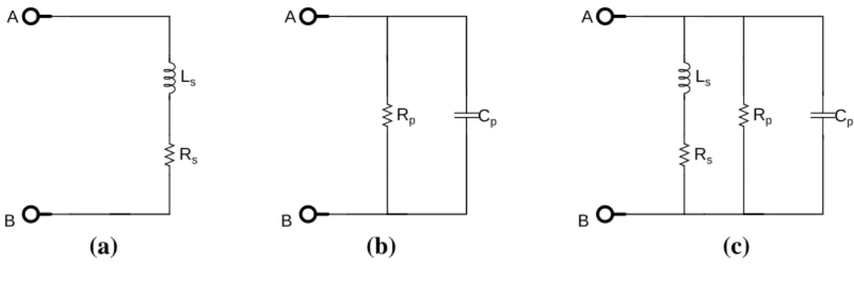
energy loss in one oscillation cycle. (2.1) For an ideal inductor and capacitor, there will be no energy loss in the system and QL and QC are infinite. A real inductor can be represented by a series
combination of an ideal inductor, Ls and a parasitic resistor Rs, as shown in
figure 2.2(a). Then, the quality factor of the real inductor can be calculated from
B A Ls Rs B A Cp Rp (a) (b) B A Ls Rs Cp Rp (c)
Figure 2.2: Inductors and capacitors, in practice, dissipate ohmic loss due to internal parasitic resistances
equation 2.1. In figure 2.2(a), the instantaneous stored energy in the inductor is,
E(t) = Lsi
2
L(t)
2 . (2.2)
For inductor current, iL(t) = Ipcos ωt, (2.2) becomes,
E(t) = LsI
2
p
4 (1 + cos 2ωt) (2.3) and the peak stored energy as
Epeak =
LsI2
p
2 . (2.4)
The energy dissipation in Rs in one cycle is
WR = Z T 0 vR(t)i(t) dt (2.5) = Z T 0 RsIp2 cos2wt dt (2.6)
= I 2 pRsT 2 (2.7) Thus, QL = 2π I 2 pLsω 2I2 pRsπ (2.8) = ωLs Rs . (2.9)
Similarly, a quality factor of a real capacitor in Figure 2.2(b) can be found as
E(t) = CpvC2(t) 2 (2.10) = CpV 2 p 4 (1 + cos 2ωt) (2.11) Epeak = CpVp2 2 (2.12) WR = Z T 0 vR(t)i(t) dt (2.13) = Z T 0 V2 p Rp cos2wt dt (2.14) = V 2 p T 2Rp (2.15) QC = ωCpRp. (2.16) where in (2.11), vC(t) = Vpcos(ωt).
When a real inductor and capacitor brought together, to form a resonant circuit, the overall quality factor, Qres can be found in terms of QL and QC as
1 Qres = 1 QL + 1 QC . (2.17)
Consider Figure 2.2(c) in the case of Rs = 0, which means an ideal inductor
parallel RLC tank circuit is
Qres = QC = ω0RpCp. (2.18)
Equation 2.17 implies that Qrescannot be larger than neither QLnor QC. Both, Q of an inductor and Q of a capacitor must be high in order to achieve high-Q
resonator. At microwave frequencies, it is not easy to construct high-Q devices since the parasitic effects increase with the frequency. Note that in equation 2.17
QL and QC are quality factors of L and C at resonance frequency, ω0.
The resonance frequency is the frequency at which the imaginary part of the impedance of the resonator becomes zero. In Figure 2.2(c), when Rs = 0, the
impedance of the parallel circuit seen from terminals A-B is given by1
Zres = 1 1 Rp + 1 jωLp + jωCp (2.19) = 1 1 Rp + j[ωCp− 1 ωLp] (2.20)
The imaginary term in the denominator of equation 2.20 equals to zero for
ω = ω0 =
1 p
LpCp (2.21)
which is the resonance frequency of the resonator.
2.3
Transmission Line Theory
Figure 2.3 shows a transmission line of length ` terminated with a load impedance, ZL. The total input impedance, Zin(z = 0) is given by [22]
Zin = Z0
ZL+ Z0tanh(α + jβ)`
Z0+ ZLtanh(α + jβ)`
(2.22)
where Z0, α and β are the characteristic impedance, attenuation constant and
phase constant of the transmission line, respectively.
1it is convenient to define L
ZL Z0, α, β
Zin
z=0 z=l
Figure 2.3: A transmission line terminated in a ZL.
For a short-circuited transmission line (ZL = 0), the equation 2.22 simplifies
to
Zin = Z0tanh(α + jβ)`. (2.23)
In the following sub-sections, equation 2.23 is examined separately in the cases of absence and presence of loss in the transmission line.
2.3.1
Lossless Transmission Line
To simplify the analysis consider the case when there is no loss in the transmission line (α = 0). Now the input impedance (Zin) becomes
Zin = Z0tanh(jβ`) (2.24)
= jZ0tan(β`) (2.25)
= j Z0β`. (2.26)
where last result was obtained by assuming β` ¿ 1. We can observe that input impedance is purely imaginary in this case and for small β`, Zin is purely
induc-tive. The inductance of the equivalent circuit can be found from equation 2.26 and using the relation Zin= jωL.
L = Z0β`
ω (2.27)
= Z0`
υp
where υp is the phase velocity, which is constant for the lossless line and
approxi-mately constant for a low-loss line[22]. Equation 2.28 implies that for a relatively small ` with respect to the wavelength, λ, the transmission line exhibits an in-ductive behaviour and, moreover, the inductance value, L, stays constant with frequency as long as the condition 2π`
λ ¿ 1 holds. Figure 2.4 shows the equivalent
circuit of a short- circuited lossless transmission line.
Z0, β
L
Figure 2.4: Equivalent circuit model of a lossless transmission line when ZL= 0.
2.3.2
Lossy Transmission Line
In real life, transmission lines dissipate some energy due to finite conductivity and lossy dielectric between the inner and outer conductors. For a lossy transmission line, the attenuation constant, α, in equation Zin= Z0tanh(α + jβ)`, should be
taken into account during analysis. If we apply an identity for the hyperbolic tangent for this equation, we get
Zin = Z0
tanh(α`) + j tan(β`)
1 + j tan(β`) tanh(α`). (2.29) Again for the cases β` ¿ 1 and α` ¿ 1 the input impedance simplifies to
Zin = Z0
α` + jβ`
1 + j β` α`. (2.30) Further analysis leads to
Zin = Z0`(α + jβ)(1 − j αβ` 2) 1 + (αβ`2)2 (2.31) = Z0α ` 1 + β2`2 1 + (αβ`2)2 + j Z0β ` 1 − α2`2 1 + (αβ`2)2. (2.32)
Note that if β` ¿ 1 and α` ¿ 1 then (β`)2 ¿ 1 and (α`)2 ¿ 1 also. Therefore
the equation 2.32 can be re-written as
Zin = Z0α` + j Z0β`. (2.33)
The equivalent circuit of a lossy transmission line is an inductor with a parasitic resistance in series. The inductance and the resistance values of the equivalent circuit are L = Z0β`
ω and R = Z0α`, respectively. The loss in the line is
repre-sented by a series resistance, R, in this case. The inductance value of a lossy transmission line is the same as in equation 2.27, which is the inductance value of a lossless line. Figure 2.5 shows equivalent circuit of a short-circuited lossy transmission line. In the next section, cavities constructed from an air-filled
Z
0,
α
,
β
R L
Figure 2.5: Equivalent circuit of a lossy transmission line when ZL = 0.
waveguides are discussed. Since waveguides are also some sort of transmission lines, similar approaches can be applied in the analysis[23].
2.4
Cavity inductors
It was shown that a short-circuited transmission line of length `, can be modeled as an inductor with a series resistance, for frequencies which satisfy the condi-tion β` ¿ 1. The same is true for a short-circuited waveguide also and for a cavity which is enclosed by conducting walls. In this thesis, cylindrical cavity constructed from copper plated walls and aluminium coated hexagonal cavity
formed by etching a silicon substrate using MEMS techniques are designed and fabricated. In this section theoretical results are presented for Q-factors and resonance frequencies of such resonators.
2.4.1
Cylindrical Cavity Inductor
Consider Figure 2.6 which shows an ordinary air-filled cylindrical cavity enclosed by conducting walls. There is a small circular slot at the left face (z = 0 plane). Energy is coupled to the cavity walls via a probe which passes through the slot and is connected to the right face of the cylinder (at z = `). Here, the objective is to find the impedance seen from terminals A and B so that the structure can be modeled by an equivalent circuit with lumped - elements. Note that, if the left and right faces are removed from the cylinder and if the probe is short-circuited by a small wire to the side wall at z = `, the cavity turns out to be a short-circuited coaxial transmission line, in which the probe forms the inner conductor and the side walls form the outer conductor of the transmission line.
A
B Air
Conductive walls
z=0 z=l
Figure 2.6: Air-filled cylindrical cavity
In section 2.3.2, it is found that the equivalent circuit of a lossy transmission line is an inductor and a resistor in series. The corresponding inductance and resistance values are also found in terms of transmission line characteristics. For
example, the series resistance, R, due to the loss in a line, is found as R =
Z0α`. All these parameters depend on the transmission line characteristics; or
by another way of saying, transmission line is characterized by these parameters. Here, Z0 is the characteristic impedance of the line. For a coaxial transmission
line, whose inner conductor radius is a and the outer conductor radius is b, the characteristic impedance, Z0, is given by [23]
Z0 =
η ln(b/a)
2π (2.34)
where η is the intrinsic impedance of the medium and also given by in terms of permittivity and permeability of the medium as η = pµ/²0. The attenuation
constant, α, is another transmission line parameter and has two components: the attenuation due to the conductor loss, αc, and the attenuation due to the lossy
dielectric αd. And for a coaxial transmission line αc and αd are given by [23]
αc = Rs 2η ln(b/a) ³ 1 a + 1 b ´ (2.35) αd = 1 2β tan δ (2.36) Rs = r πf µ0 σ (2.37)
where Rs is the surface resistivity of an imperfect conductor. Here, it is worth
to mention that in practice, the attenuation due to conductor loss is, generally, slightly bigger. This is because, in practice conductors do not have perfectly smooth surfaces. A rough surface causes a loss and therefore the attenuation increases. The following formula can be used to compensate the loss due to the surface roughness [24] α0 c= αc · 1 + 2 πtan −1 1.4³∆ δs ´2¸ (2.38) where α0
c is the corrected attenuation constant for rough surfaces, ∆ is the rms
Note that for an air-filled line αd = 0 and α = αc. From these results, a
resistance, R = Z0α`, in the equivalent circuit model becomes
R = η ln(b/a) 2π r πf µ0 σ 1 2η ln(b/a) ³ 1 a + 1 b ´ ` (2.39) = 1 4 r f µ0 πσ ³ 1 a + 1 b ´ `. (2.40)
Similarly, the inductance value, L = Z0`
υp , can be found as L = η ln(b/a) 2π ` √ µ² (2.41) = µ` ln(b/a) 2π . (2.42)
Now if we consider the air-filled cavity including with left and right faces as in the Figure 2.6, the impedance seen from port A and port B (which are shown in the figure) would be (not surprisingly) an inductor with an associated parasitic resistance. In this case, the equivalent resistance will be increased due to the power loss on the surfaces of left and right faces. It would be worth to say that in the previous discussion of lossy coaxial transmission line, energy loss through radiation was ignored. In a shielded cavity, the electromagnetic fields are completely confined inside the cavity and therefore, radiation losses are kept very low compared to coaxial transmission line.
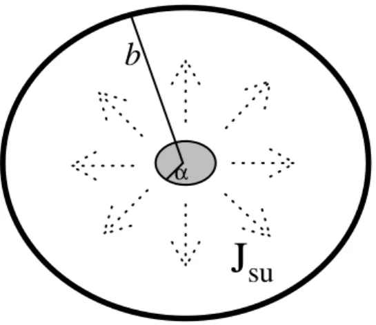
Resistance of the left and right faces can be found from dissipated power on the surfaces. In Figure 2.7 current is generated at the center of the circular plate and flows in the radial direction. Here, it is assumed that the current flows in a very thin surface layer and therefore the corresponding current density, Js
ap-proximately equals to Jsu, surface current density. This is a good approximation
as long as the conductivity of the faces and the operating frequency are very high; or skin depth is very low. Since there is power dissipation in the left and right faces, there should be non-zero radial electric field, arEr, at the surfaces in
b
α
J
su
Figure 2.7: Power dissipation occurs on the surface of a imperfect circular con-ductor.
be
pσ = 1
2<{|Jsu|
2Zs} (2.43)
where Zs is the intrinsic impedance of the surface and equals to [22] Zs = (1 + j)
r
πf µ
σ (2.44)
for a good conductor. If we put equation 2.44 into equation 2.43, we get
pσ = 1 2|Jsu| 2 r πf µ σ . (2.45) Surface current I is I = Z 2π φ=0 Jsur dφ (2.46) = Jsu2πr (2.47)
And the power dissipated on one of the faces is
P = Z S pσds (2.48) = 1 2 r πf µ σ Z 2π φ=0 Z b r=a I2 (2πr)2r drdφ (2.49)
= I21 4
r
f µ
πσln(b/a). (2.50)
Hence, the effective series resistance for one face is found as
Rf ace= 1
4 r
µf
πσln(b/a). (2.51)
Similarly, from the complex power dissipated on the surface and using equation 2.44, the effective inductance can be found as
ωLf ace = 1 4 r πf µ σ ln(b/a) (2.52) Lf ace = 1 8π r µ πf σln(b/a). (2.53)
Note that this inductance can be negligible compared with the inductance value given in equation 2.42, when the conductivity of the surface and the operating frequency are high enough. Figure 2.8 shows the equivalent circuit of the cavity given in Figure 2.6. For total inductance, LT≈L, and total resistance, RT =
A B Air z=0 z=l B A A L R Lface Rface Lface Rface
Figure 2.8: Equivalent circuit with lumped - elements.
R + 2Rf ace the quality factor, Q of the inductor will be
Q = ωLT RT (2.54) = 2πf µ0` 2π lnab 1 4 q f µ0 πσ ³ 2 ln b a + ` a + ` b ´ (2.55)
= 4 `pµ0f πσ lnb a 2 ln b a + ` a + ` b (2.56) = 4 ` δ(f ) lnb a 2 lnb a+ `a+ `b (2.57)
2.4.2
Silicon Cavity MEMS Inductor
In the previous section, a shielded cylindrical cavity is discussed. The structure is modeled by lumped circuit elements and parameters in the circuit model are found. In this thesis, another similar type of cavity was fabricated by microma-chining silicon substrate. Silicon was used because it is easy to utilize MEMS techniques on it. By selectively removing (etching) substrate of the silicon, a cavity inside the substrate can be constructed. However, such a cylindrical cav-ity structure as in Figure 2.6 is very hard to achieve due to the nature of the crystallographic structure of Si. Therefore, not a cylindrical but hexagonal cav-ity was fabricated which is easier to realize. Here, the important thing is not the shape of the cavity but cavity itself. A cavity enclosed inductor has low-loss at high frequencies. On the other hand, in a printed inductor (when there is no cavity), losses due to the silicon substrate significantly reduce the performance of the device as the frequency increases. Thus, an inductor enclosed in an air-filled cavity is constructed to obtain a low-loss inductor.
There are various silicon substrate etchants in the literature. Most common of them are HNA (hydrofluoric acid, nitric acid and acetic acid), EDP (ethylene-diamine and pyrocatechol), TMAH (tetramethyl ammonium hydroxide), DRIE (deep reactive ion etch) and KOH (potassium hydroxide). Etching of a sub-strate in a liquid etchant such as HNA, EDP, TMAH and KOH is referred to as wet etching. On the other hand, DRIE is an example of dry etching where the etchants (reactants) are in plasma state. Etching processes are also catago-rized in terms of being isotropic or anisotropic. Depending on the type of the
etchant and crystallographic structure of substrate the etching process can be either isotropic or anisotropic. In anisotropic etching, etch rates of different crys-tallographic planes differs, while in isotropic etching etch rates of different planes are equal. HNA etch of silicon is an example of isotropic etching where etchants attack to the silicon surface at the same rates in all directions. KOH etching of silicon is an example of anisotropic etching where etch rate in the h110i direc-tion is about more than 500 times of the etch rate in the h111i direcdirec-tion which provides achieving of different shape of structures[25].
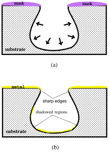
Since silicon is a poor conducting material, cavity walls must be shielded by a good conductor such as gold, copper, alminium, etc. The critical issue here is that after metal is plated to the walls of the cavity, the continuous electri-cal conductivity between the walls must be established, which is not so easy in some cases. The situation can be explained better from Figure 2.9. In the figure, substrate is selectively etched by using isotropic etchant and appropriate masking. However, during isotropic etching, as it is shown in the figure, some regions, which are under the etch mask, are also etched horizontally. This sit-uation is often undesirable. In the isotropic etching, as reactants etch through the substrate, they attack in all directions at the same etch rate which makes isotropic etching impractical for some applications (as in our case). After etch-ing of substrate is completed, a cavity is formed. However, as mentioned earlier, conductivity of a silicon substrate is very low and therefore the side walls must be deposited by a good conductor. During deposition of a metal (usually done by evaporation), undercut regions are shadowed by the masking area and metal could not be deposited onto those regions. Sputtering might help to solve this shadowing problem but it is still difficult to achieve a continuous conductivity at places where sharp edges found. On the other hand, anisotropic etching of silicon can also be utilized to construct a cavity inside the substrate. KOH (potassium hydroxide) and water mixture is well-known, frequently used wet etching solu-tion. KOH etching of (100) silicon makes an angle of 54.7◦ between the plane
mask mask substrate substrate shadowed regions metal sharp edges
(a)
(b)
Figure 2.9: Isotropic etching and metal deposition (side view). (a) Same etch rate in all directions. (b) Unsuccessful metal deposition due to the sharp edges and undercut.
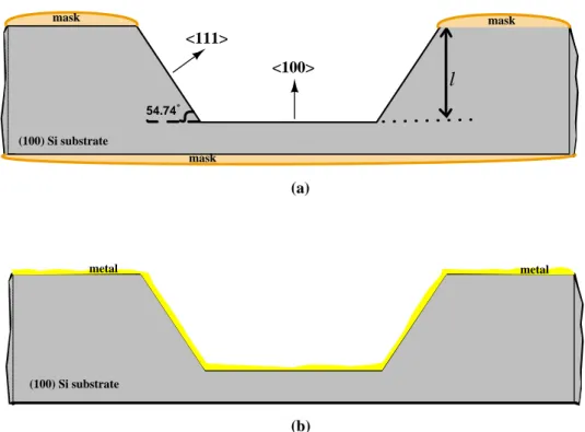
of the wafer and the {111} plane[26], as shown in Figure 2.10(a). Note that after metal deposition, in this case, electrical conductivity can be easily obtained between the cavity walls. However, now, from Figure 2.10(b) and Figure 2.11 it can be seen that the opening at the top surface of the silicon substrate becomes wider which can cause radiation loss.
Another issue is the depth of the cavity, `, which is limited by the substrate thickness. In equations 2.42 and 2.57, the values of inductance, L, and the quality factor, Q, are proportional with the depth of the cavity. Thus, the deeper cavity means higher inductance and higher Q-factor. One of the possible approaches
mask mask (100) Si substrate <100> <111> 54.74˚ (100) Si substrate metal metal (a) (b) mask l
Figure 2.10: Anisotropic KOH etching of (100) Silicon and metal deposition (Side view). (a) Etch rate in h100i significantly larger than etch rate in h111i direction. (b) Successful metal deposition.
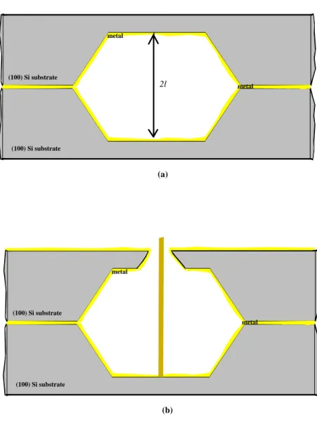
to increase the depth of the cavity is shown in the next figure. Here, KOH etched and gold (or any other metal) deposited Si substrate is turned upside down and placed on the top surface of another substrate. In this structure, the depth of the cavity increases twice while the opening becomes much narrower. By using this method, from bulk of the silicon, not cylindrical but hexagonal cavity with metallic walls can be fabricated. As in the cylindrical inductor, an opening can be made at the top of the substrate so that a probe is inserted into the cavity (Figure 2.12(b)). The final structure offers a high-Q MEMS inductor at microwave frequencies. In this thesis, the structures in Figures 2.8 and 2.12 are fabricated. The dimensions of the cavities are a = 0.5 mm, b = 10 mm,
` = 11 mm and a = 12.5 µm, b = 3000 µm, ` = 900 µm, respectively. The
resonator circuit is achieved by connecting external chip capacitor in parallel to the terminals A and B of the cylindrical cavity.For the silicon cavity, a MIM
{111}
Figure 2.11: Anisotropic KOH etching of (100) Silicon. Metal is deposited to side walls of the cavity (Top view).
capacitor is fabricated on the top surface of the silicon substrate, next to the opening where probe is inserted. Note that the dimensions of the cylindrical cavity are very large compared to silicon cavity so that it cannot be integrated in a single chip. It is worth to mention that the purpose of the cylindrical cavity fabrication is to verify the equations that are found in 2.57 and 2.42. In the next chapter, the results of the cylindrical cavity is presented.
(100) Si substrate (100) Si substrate metal metal (a) (100) Si substrate (100) Si substrate metal metal (b) 2l
Figure 2.12: Two silicon substrate is combined face to face (Side view). (a) The cavity is formed. (b) An opening can be made at the top surface of the cavity to couple the energy.
Chapter 3
CONSTRUCTION AND
MEASUREMENT RESULTS
OF A LARGE SCALE
CYLINDRICAL CAVITY
RESONATOR
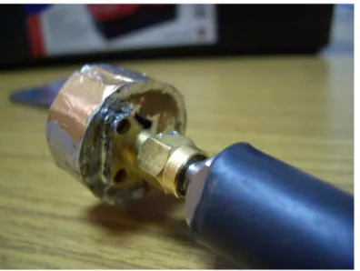
An air-filled cylindrical cavity was fabricated from 0.1 mm thick copper plate in order to verify the inductance and Q-factor equations given in chapter 2. The energy is coupled into the cavity via a SMA coaxial connector placed at the center of one of the side face of the short-circuited cavity. The probe of the SMA, penetrating into the cavity, was connected to the other side face of the cylinder. An external chip capacitor, is soldered between the probe and the ground of the SMA connector. The photographs taken during measurements can be seen from Figures 3.1, 3.2 and 3.3.
Figure 3.1: Photograph of cylindrical cavity.
The dimensions of the cylinder was as follows: b = 10 mm, a = 0.5 mm and
` = 11 mm. From equations 2.57 and 2.42, the inductance value, L, and the
corresponding quality factor, QL can be calculated as
L = µ0`
2π ln(b/a)
L = 6.59 nH Q(f = 1GHz) = 2200
The capacitance value of the chip capacitor was 5.6 pF. The next four figures show the results of the measurements of cylindrical cavity resonator. Measure-ments were done by using HP 8753D Vector Network Analyzer.
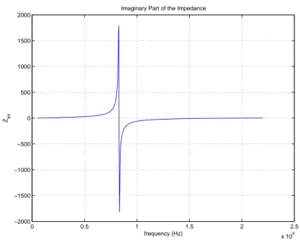
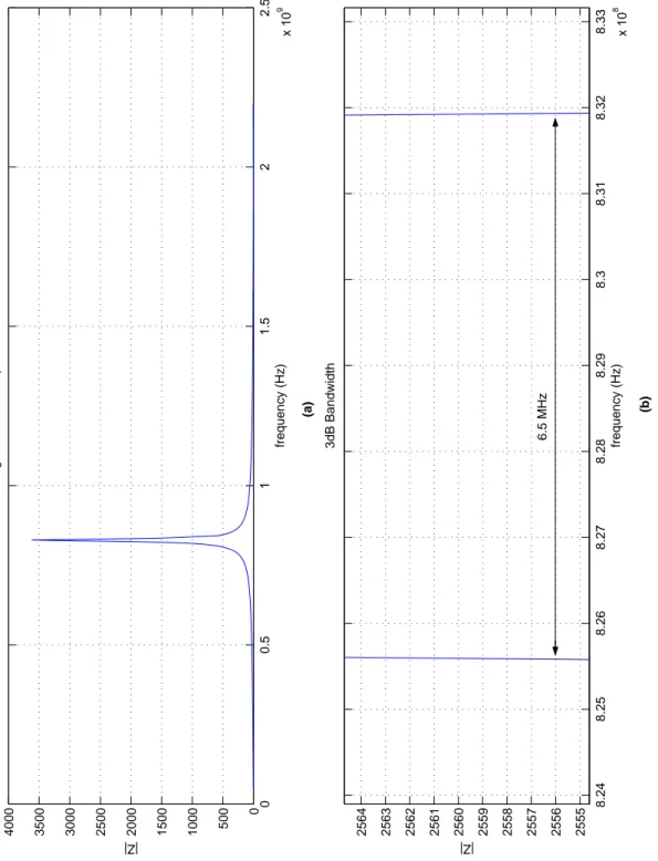
The resonance frequency, fres, was measured as 830 MHz. Then, the
induc-tance value can be found as
L = 1
ω2
0C
(3.1)
Figure 3.2: Photograph of cylindrical cavity.
Note that, this value is very close to the computed inductance value using equa-tion 2.42. On the other hand, the quality factor was measured as,
QL = fres ∆f3dB (3.3) QL = 830 6.5 (3.4) QL = 128 (3.5)
which is far from the calculated value. Although every effort was undertaken to make the impedance measurement as precise as possible, the measurement accuracy was limited by the accuracy of the calibration sets. Even under these circumstances, the measured Q is very high and is obviously limited by the Q of the capacitor. The calculated value of the Q (2200) is very difficult to measure by using network analyzer at these frequencies and it is certainly beyond the scope of this thesis. The main obiective behind this exercise of building a large scale model was two-fold; to verify the inductance and quality factor formulas to some extend and to develop and try the Q measurement methodology. The
Figure 3.3: Photograph of cylindrical cavity.
result was encouraging, so we progressed to develop, fabricate and measure the actual on-chip resonator.
0 .4 1 2.5 5 20 0 .4 1 2.5 5 20 0 .4 1 2.5 5 20 start frequency: 50 MHz stop frequency: 2.2 GHz C=5.6 pF
Cylindrical cavity resonator
0 0.5 1 1.5 2 2.5 x 10⁹ −500 0 500 1000 1500 2000 2500 3000 3500 4000
Real Part of the Impedance
frequency (Hz) Zre
Figure 3.5: Real part of the impedance.
0 0.5 1 1.5 2 2.5 x 10⁹ −2000 −1500 −1000 −500 0 500 1000 1500 2000
Imaginary Part of the Impedance
frequency (Hz) Zim
0 0.5 1 1.5 2 2.5 x 10 9 0 500 1000 1500 2000 2500 3000 3500 4000
Magnitude of the Impedance
frequency (Hz) |Z| 8.24 8.25 8.26 8.27 8.28 8.29 8.3 8.31 8.32 8.33 x 10 8 2555 2556 2557 2558 2559 2560 2561 2562 2563 2564 3dB Bandwidth frequency (Hz) |Z| 6.5 MHz (a) (b)
Chapter 4
DESIGN AND FABRICATION
OF SILICON CAVITY
RESONATOR
4.1
Device Design
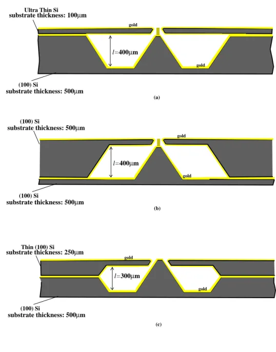
At the beginnning of the project, different cavity structures were considered. Several of them are shown in Figure 4.1. Note that, in these structures it is possible to achieve completely enclosed cavities by bonding two etched substrates together. In the litreature, bonding of two wafers was realized by [27, 28, 29, 11, 14]. However, note also that cavity depths are limited by a thickness of a single wafer. The reason of this limitation is the following: just under the opening, a small part of the top surface is not removed by using an appropriate mask which causes a pyramid shape structure at the center of the substrate in KOH etching of (100) Silicon. Pyramidal structure is used as a probe to couple the energy into the cavity. Since the height of this structure should reach from bottom to top surface (which is the substrate thickness), the cavity depth cannot
(100) Si (a) Ultra Thin Si substrate thickness: 100µm substrate thickness: 500µm l=400µm (100) Si (b) substrate thickness: 500µm l=400µm substrate thickness: 500µm (100) Si gold gold gold gold (100) Si (c) Thin (100) Si substrate thickness: 250µm substrate thickness: 500µm l=300µm gold gold
Figure 4.1: Silicon cavities achieved by bonding of two substrates.
exceed that limit. The base area of this structure becomes larger and the cavity becomes smaller as the substrate is etched further. This reduces the associated inductance value of the cavity. In fact, it is very hard to realize such a small pyramidal structure at the center of the cavity while etching down the substrate about 400 µm. This is because of undercutting of convex corners during KOH etching of Si. Corner compensation techniques are also not very practical in this case since the dimensions of the compensating structures exceed the dimensions of the cavity resulting in unsuitable masking of the substrate. Using a thick
wafer (such as a substrate thickness of 1000 µm) is not convenient due to the same problems. Therefore, these structures were omitted at the design stage and were not fabricated.
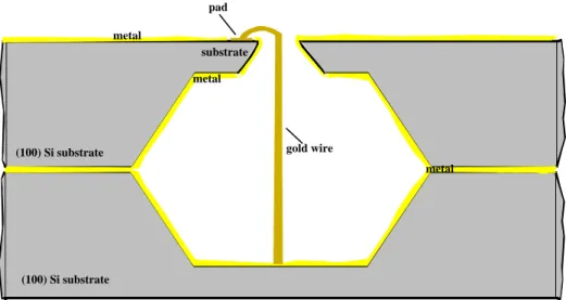
Consider the structure in Figure 4.2 where one end of the gold wire is
con-(100) Si substrate (100) Si substrate metal metal pad gold wire substrate metal
Figure 4.2: Initial design.
nected to the pad on top of the substrate while the other end is connected to the base of the substrate. Since lightly-doped silicon is poor conductor, at DC there is no electrical connection between the pad and the metal-coated walls through substrate. Obviously, there is a connection through the wire. This structure, compared to the ones in Figure 4.1 offers many advantages. As stated before, the cavity depth increases by two which significantly enhances the quality factor and the inductance value of the inductor. Energy is coupled via a gold wire, hence, there is no pyramid shape structure and consequently no convex corners compensation is needed. A low-cost, lightly-doped, typical silicon wafer having a thickness of 500 µm can be used for both top and bottom substrates. Therefore, we considered these advantages and decided to fabricate this structure. But, as shown in Figure 4.2, there is no capacitor in the structure. This is because in the design stage, our first intention was to fabricate high-Q inductor that can be
used at microwave frequencies rather than a resonator. A resonant circuit would be easily realized by connecting a high-Q chip capacitor or a varactor between the pad and the metal walls at the top surface.
During the fabrication of the above structure, we encountered some difficul-ties, however, and therefore, the structure was changed several times. The main problem was the substrate loss of silicon. When a signal was applied between the pad and the metal walls on the top surface, there was a significant loss due to the lossy substrate under the pad. Fields penatrating from the pad to the walls get experienced a substrate loss, which results in significant degradation in the qual-ity factor of the inductor. This is shown in Figure 4.3. Note that metal-coated walls completely shield electromagnetic waves inside the cavity from the lossy substrate and thus, there was no such loss. Several approaches were used to
pre-pad metal
substrate field
Figure 4.3: Substrate loss
vent the loss. One of them was coating a low-loss dielectric just under the pad. BCB (benzocyclobutane) was used for this purpose. BCB has been developed for high frequency MEMS applications by The Dow Chemical Company [30]. It is easy to coat and exhibit very small loss-tangent compared to silicon substrate.
As a result of this improvement, the loss becomes less but was still an unaccept-able level. In chapter 5, the smith chart plots are given for each device tested. Then, PECVD silicon nitride was deposited as an alternative low-loss dilelectric instead of BCB, but almost similar results were obtained. A better approach was needed in the design to reduce the substrate loss. We decided to shield the entire top surface as we did at the cavity walls. At this point the structure turned out to be a resonator. Because a MIM (metal-insulator-metal) capacitor should be placed, in this case, to provide an isolation between the signal pad and the metallic walls on the top surface. And the parallel combination of the MIM capacitor and the inductor acts as a resonant circuit. The final structure is given in Figure 4.4. By this way, both reduction in loss and the realization of an on-chip resonator are established at the same time.
(100) Si substrate (100) Si substrate
metal metal
(a)
MIM (Au/Si3N4/Au) capacitor
gold wire metal substrate (b) dielectric metal
Figure 4.4: (a) RF MEMS Cavity Resonator. (b) MIM capacitor at the top of the cavity
There were also other problems which have effects on the performance of the device. For example, bonding of the gold wire shown in the structure at the bottom substrate requires vertical deep access wedge bonder or a ball bonder equipment. Therefore, the width of top opening must be sufficiently large for the bonding tool to access the deep cavity. Also, bonding onto the pad area was very problematic since the required force for making successful bonding was
strong enough to smash the MIM capacitor under the pad. Therefore, bonding to the top surface was done by using a silver epoxy which, certainly, causes a loss. Silver epoxy was also used in bonding of the two substrates although a better way of bonding two wafers is a thermocompression bonding as in [14]. Due to such limitations in the fabrication processes, the resonator was designed accordingly. As the future work, if these problems are solved, the quality factor of the resonator will be considerably enhanced.
This structure was fabricated in the Advanced Research Laboratories - Class 100 Clean Room. And the measurements were done by using HP 8753D Vector Network Analyzer in our department. Results showed that an on-chip high-Q resonator at microwave frequencies can be fabricated by using this geometry. Moreover, it is possible to make a tunable resonator if a MIM capacitor is replaced by a varactor. Also, Q-factor can be improved further by changing a few steps during fabrication.
4.2
Physical Dimensions of the Device
In this section, dimensions of the cavity, the gold wire and the capacitor is given. Theoretical values of the capacitance value, C, the inductance value, L, and the corresponding quality factor, QL and the resonance frequency, ω0, of the
resonator are also calculated using the equations given in chapter 2.
In Figure 4.4(a), the structure of the cavity resonator is given. In the figure, the width of the openning at the top surface seems very narrow compared to the depth of the silicon. However, as described in section 4.1, this opening should be large enough so that the bonding tool can be inserted from the opening and reach to the base of the cavity. Therefore, the width of this opening is limited by the tool that is used. There are special tools in the market for deep access bonding processes. For example Deweyl Tool Company provides vertical access
tool whose bottom width is only 230 µm which means an opening of 300-350 µm is fairly enough to insert the tool and make contact to the base[31]. However, in our case, Kulicke & Soffa ball bonder was available and used. In this manner, the opening had to be kept relatively larger. Figure 4.5 shows the dimensions of the structure. In the figure, the substrate thickness is given as 500 µm. The
w l α b 500µm 54.74˚ 100µm 100µm √Α 50µm d pad metal dielectric
Figure 4.5: Physical dimensions of the cavity resonator (Side view).
bottom substrate is etched until a thickness of 100 µm left. Note that, the top substrate is completely etched away to make an opening at the surface. The width of the opening is denoted by w. In the fabrication, w was chosen to be about 650 µm. The depth and the radius of the cavity are denoted by ` and b, respectively. The radius of the wire, also, has an important effect on the values of inductance and Q-factor and denoted by a. From equation 2.57, it can be seen that a high-Q inductor can be realized by choosing the radius of the wire large which reduces the conductor loss. However, the bonding equipment that was used in this work is compatible with the wire of diameter 25 µm. Therefore, in our case, a = 25 µm2 =12.5 µm. As shown in the figure, depth of the cavity,
`, is 900 µm. Finally, the radius of the cavity, b, can be chosen without any
increases, sizes of the device and chip also increase. In this thesis, b was chosen as 1500 µm. If these values of a, b, ` are put into equations 2.42 and 2.57, the approximate inductance and Q-factor values of the cavity can be calculated as,
L = 0.9 nH (4.1)
QL = 171 (4.2)
at 4.5 GHz and for aluminium coated walls. Note that equations 2.42 and 2.57 are found for cylindrical cavity, not for the structure given in Figure 4.5. Another point is that, in this geometry the length of the gold wire is not equal to the depth of the cavity, which is the case in Figure 2.6. The length of the wire has, certainly, an effect on the inductance value L. Therefore, the theoretical calculations given in this section deviate from the experimental results.
The dimensions of the paralel-plate capacitor is also shown in Figure 4.5. Plates are in the shape of a square. The one edge of the square is given as √A,
where A is the pad area. The capacitance value, C, is directly related with the size of A and the thickness of the dielectric material, d. As stated before, the pad area should be large enough to make a successful bonding of the wire. To serve this, the edge of the pad area was set to minimum 175 µm. Bigger pad can also be used to increase the capacitance. At this point, the thickness, d, and the associated dielectric constant of the dielectric material become important. In the fabrication, Si3N4 (silicon nitride) film and BCB were used as the dielectric
material where the dilectric constants of Si3N4film and BCB are between 6-9 and
2.5-2.75, respectively [2, 32, 30]. Therefore, different thicknesses and area sizes were employed during fabrication of capacitance. For BCB layer, approximate sizes were d=8 µm, √A =750 µm and ²BCB = 2.7, from which capacitance
becomes C = ²0²rAd = 1.68 pF. For Si3N4 film, d=1.5 µm,
√
A =175 µm and
C = ²0²rAd = 1.37 pF for ²r = 7.6. Finally, the resonance frequncy can be found
4.3
Fabrication Processes
In section 4.1, evolution of the device is discussed. There were considerable variations in the final and initial structures which cause corresponding changes in the fabrication processes also. Some parts of the structure were already designed before fabrication processes, such as KOH etching and metal deposition, while some parts had to be changed due to troubles that were encountered during fabrication such as bonding of wire to top surface. In this section, description of the processes that we employed during fabrication are presented. A process, usually, can be realized by utilizing different techniques. Reasons of why a specific technique was chosen for a particular process and, advantages and disadvantages of that technique compared to others are given including associated results. The section begins with describing etching process of silicon and continues with other processes by following the same order of fabrication steps.
4.3.1
Etching of Silicon and Masking
A cavity inside a bulk silicon can be constructed by selectively remov-ing significant amount of silicon from substrate. The most common bulk silicon etchants are TMAH (tetramethyl ammonium hydroxide), EDP (ethylenediamine-pyrocatechol) and KOH (potassium hydroxide)[33]. All these etchants are orientation-dependent, (often called anisotropic), meaning that etchants etch much faster in one direction than in another, revealing the slow-est etching crystal planes over time[28]. In the literature, several reasons of anisotropic behaviour are presented. In [25], one of the most important reason is given as the atomic lattice packing density and available bonds in the crys-tallographic structures of silicon. (111) plane exhibit very high atomic packing density compared to (110) and (100) planes. Therefore, etch rate in the h111i direction considerably very low compared to etch rates in the h110i and h100i
directions. Furthermore, the atomic packing density of (110) plane is less dense than that of (100) plane which results in higher etch rate in the h110i direc-tion. On the other hand, in [28], another reason of this anisotropy is specified as screening of the surface by attached H2O molecules, which is determined by
crystal orientation. Another approach can be found in [34, 1]. (110) surface has a more uneven atomic structure than the (100) and (111) surfaces. (111) is tightly packed and has only one dangling bond while the other three bonds remaining in the crystal. The atoms on the (100) plane have two dangling bonds while the other two bound to the crystal. The importance of the dangling bonds is the following: during etching process, hydroxide ions in the etchants, such as OH− in
KOH, can attach to the dangling bonds of an atom and weaken the other bonds that are in the crystal. Therefore, it becomes easy to break an atom from the surface. Since there are two dangling bonds per atom in the (100) plane, it is etched faster.
Comparison of Bulk Silicon Etchants
Anisotropic etching of silicon forms a basis for the resonator structure. It was important to realize a cavity at first. Therefore, in this thesis, most conve-nient method was preferred to etch the substrate. The choice of etching solution depends on many factors, such as etching rate, anisotropy, cost, selectivity of silicon compared to masking film and surface roughness. In this manner, among the many kinds of etchants, solution of KOH and H2O was employed during
fabrication. One of the other candidates was EDP. EDP (also referred as EPW for ethylene diamine, pyrochatechol and water [35]) is classic but very hazardous and corrosive, and also, its vapor is carcinogenic, therefore it is hard to deal with [28, 36]. On the other hand, TMAH is easy to use and has many advantages. It allows utilizing SiO2 as an etchant mask and etching of silicon after CMOS
alkali hyroxide etchant used in silicon bulk etching. The key advantages of KOH are low-cost, safe, repeatability and uniformity which allows batch fabrication . However, there are drawbacks of using KOH also. Main drawback is the creation of H2 gas bubbles during etching. As a result of redox reaction, formation of H2
gas bubbles onto the surface of the substrate occur [34]. The redox reaction of KOH etching of silicon is given as [28]
Si+2OH− −→ Si(OH)++2 + 4e−
Si(OH)++2 + 4e−+ 4H2O −→ Si(OH)−−6 + 2H2.
First the oxidation takes place. Silicon bonds are broken and the silicon is ox-idized which results in accumulation of four electrons from each silicon atom into the solution. Then, water is reduced and leading to the formation of H2
gas molecules. The size of the H2 bubbles and the duration they remain onto
the substrate surface depend on the KOH concentration and temperature of the solution. Longer duration of existance of large bubbles onto the surface can stop etching and act as a pseudomask, which increases the surface roughness [38, 34, 39, 29, 40]. The followings can also be considered as other two draw-backs of using KOH: It etches aluminium and therefore, is not compatible with the CMOS devices; and the problem of convex corner undercutting of (100) sili-con in KOH can be quite serious [41]. Surface roughness and corner undercutting problems can be avoided by utilizing appropriate techniques. In particular, as KOH concentration and temperature are increased, the diameter of the bubbles produced decreases. Small bubbles leave the surface much faster and KOH can etch the surface. The small bubbles, therefore, cause less rough surface compared to large bubbles [42]. The surface tension of the KOH solution is, also, important for the surface roughness. The surface tension arises from the polar nature of the molecules. For any liquid, lower surface tension means better wetting capability and high degree of attraction with which it has contact. Surface tension of water can be reduced significantly by increasing temperature. In the literature, it is also well known that isopropyl alcohol (IPA) is used in KOH and TMAH solutions
to improve the surface smoothness by decreasing surface tension[40, 43, 44, 37]. Mechanical stirring and megasonic sound will remove the hydrogen bubbles from the surface also. Further improvements can be found in [45]. The other draw-back, convex corner udercutting can be avoided by using corner compensation techniques. There are many different compensation techniques. Some of them can be found in [46, 47, 48, 35, 49, 50, 51]. Since, in our case, there are no convex corners and the surface roughness is not a very critical problem as long as the electrical conductivity between the cavity walls is achieved after metal deposition, KOH was a good choice to be used in the fabrication.
KOH Concentration and Temperature
In the previous discussion, it is mentioned that the surface roughness of the etched areas depends on the KOH concentration and the temperature of the so-lution. However, in addition to the surface roughness, the concentration and the temperature play a key role on the etch rates of the different crystallographic planes. There are many presented work about the KOH etch rates for different concentrations and temperatures [52, 26, 38, 53, 54]. Table 4.1 shows etching rates along various crystallographic directions of Si for KOH concentrations of 30%, 40% and 50% at 70◦C. Table 4.1 is reproduced from [1]. In the table, etch
rates are given in µm min−1 and the numbers in parantheses are the
normal-ized etch rates relative to (110) plane. It can be seen that as the concentration increases from 30% to 40% and 50%, etching rates decrease for the same temper-ature (except the etch rate of (111) plane which is already very low compared to other planes). Increasing temperature of the solution significantly speeds up the etching rates [54, 42]. In the fabrication, we used KOH concentrations of 23.4 wt% solution which was obtained by 120 gr KOH pellets and 330 gr distilled water at 88◦C. The solution was aggressively agitated by spinning a magnet at a
Crystallographic Rates at different KOH Concentration Orientation 30% 40% 50% (100) 0.797 (0.548) 0.599 (0.463) 0.539 (0.619) (110) 1.455 (1.000) 1.294 (1.000) 0.870 (1.000) (210) 1.561 (1.072) 1.233 (0.953) 0.959 (1.103) (211) 1.319 (0.906) 0.950 (0.734) 0.621 (0.714) (221) 0.714 (0.491) 0.544 (0.420) 0.322 (0.371) (310) 1.456 (1.000) 1.088 (0.841) 0.757 (0.871) (311) 1.436 (0.987) 1.067 (0.824) 0.746 (0.858) (320) 1.543 (1.060) 1.287 (0.995) 1.013 (1.165) (331) 1.160 (0.797) 0.800 (0.619) 0.489 (0.563) (530) 1.556 (1.069) 1.280 (0.989) 1.033 (1.188) (540) 1.512 (1.039) 1.287 (0.994) 0.914 (1.051) (111) 0.005 (0.004) 0.009 (0.007) 0.009 (0.010)
Table 4.1: Etch Rates of silicon crystallographic planes for different KOH con-centrations at 70◦C. Reproduced from [1].
rate of 500 rpm. 400-450 µm substrate was etched using this solution in approx-imately six hours. Notice that this solution is about 23% KOH by weight since the KOH pellets normally contain 10 to 15% water [41]. As stated before, the addition of IPA to the solution improves the surface uniformity which reduces the requirement for stirring. However, the boiling point of IPA is 82◦C [55] which is
below the solution temperature and it is not very convenient to add IPA to 88◦C
solution. Isopropyl alcohol also reduces the etching of (110) considerably (in [56] it is given that by 90%) and (100) plane slightly but accelerates the etching of (111) plane [41].
KOH Masking
In a silicon bulk micromachining process, depending on the choice of etchants, silicon nitride (Si3N4) or silicon dioxide (SiO2) film layers are commonly used as
an etch mask. In KOH etching, deposition of thin film Si3N4 is adequate onto the
substrate. Although SiO2is also less selective compared to silicon, etching of SiO2
becomes observable especially in deep etching processes. Deposition of Si3N4 on
a Si substrate is typically made by either using PECVD or LPCVD techniques. It is known that PECVD nitride is less selective compared to LPCVD nitride [32]. The etching rates of Si3N4 made by LPCVD and PECVD are given in [57]
as 10 ˚A/hr and 400 ˚A/hr for 30% KOH at 70◦C, respectively. PECVD nitride
has many pinholes and is not very suitable as an etch mask for removing 400-450
µm silicon substrate. Futher comparison of LCPVD and PECVD Si3N4 can be
found in [32, 41].
The first step of the fabrication was deposition of LPCVD Si3N4 film onto the
500 µm thick, SSP (single side polished), (100) silicon wafers. This process was done in T ¨UB˙ITAK Y˙ITAL Laboratories at Gebze. A stoichiometric nitride film was deposited onto the both sides of the wafer, at 800◦C. A film thickness was
50 nm, which is pretty sufficient to etch the substrate 400 µm deep. A thicker film causes additional tensile stress on the wafer. There are also techniques to realize low stress (silicon-rich) LPCVD nitride films for reducing the stress while keeping the same KOH etch rate [58].
Here, it is worthwhile to mention that DSP (double side polished) wafers would be more appropriate for the fabrication rather than SSP wafers. The problem was not the deposition of Si3N4 films onto unpolished surface but, as
discussed in the following sections, was in the processes of standard photoresist spinning and lithography, and, especially, in metal deposition, in which loss due to the surface roughness is increased. It is hard to employ these processes to such unpolished surfaces. As a summary, if we emphasize again, LPCVD Si3N4
film onto both sides of the SSP wafer was successfully deposited and used as a mask in the fabrication steps followed.
4.3.2
Lithography and Mask Design
After deposition of Si3N4 films, the wafers were diced into 1 cm x 1 cm individual
pieces in METU MET Laboratories using a die saw. Then, lithography was done at the Bilkent University Advanced Research Labs. The substrate of some of these dies were removed completely to realize the upper half of the cavity shown in Figure 4.5, while the lower half was etched about 400 µm. Therefore, during lithography processes different mask patterns were employed for these two cases. After standard photoresist spinning and lithography, the Si3N4 films at
the exposed regions were selectively removed by RIE (reactive ion etching). For RIE etching of Si3N4, PR acts as a mask. The PR spin and RIE etch processes,
in this step, were employed to the unpolished side. Polished side was kept for capacitor fabrication where surface roughness is more serious.
In section 4.2, the width of the openning, w, in Figure 4.5, is given as 650 µm. The required width in the mask pattern can be calculated from Figure 4.6(a)
w mask = w + 2 500 µm
tan 54.74 (4.3)
= 1350 µm. (4.4)
Therefore, in order to achieve 650 µm wide opening at the other side of the substrates after KOH etching, 1350 µm wide Si3N4 must be removed from the
top surface. The substrates were left into the KOH solution for about 1.5 hours leading to 100 µm substrate etching. Then, another lithography and RIE pro-cesses were employed to remove Si3N4 from regions that remain inside the cavity.
By this way, cavity volume can be increased. Figure 4.7(a) shows this step. Note that, the thickness of Si3N4 in Figures 4.7 and 4.6 is only 50 nm and, for