2016 IEEE 36th International Conference on Electronics and Nanotechnology (ELNANO)
132
Effect of Substrate Temperature and Ga source
Precursor on Growth and Material Properties of GaN
Grown by Hollow Cathode Plasma Assisted Atomic
Layer Deposition
Ali Haider, Seda Kizir, Piter Deminskyi
Oleksandr Tsymbalenko, Shahid Ali Leghari, Necmi Biyikli
National Nanotechnology Research Center (UNAM) Institute of Materials Science and Nanotechnology
Bilkent University, Bilkent, Ankara, Turkey [email protected]
Mustafa Alevli, Nese Gungor
Department of Physics, Faculty of Arts and Sciences, Marmara University, Goztepe, Istanbul, Turkey
Abstract — GaN thin films grown by hollow cathode
plasma-assisted atomic layer deposition (HCPA-ALD) at two different substrate temperatures (250 and 450 °C) are compared. Effect of two different Ga source materials named as trimethylgallium (TMG) and triethylgallium (TEG) on GaN growth and film quality is also investigated and reviewed. Films were characterized by X-ray photoelectron spectroscopy, spectroscopic ellipsometery, and grazing incidence X-ray diffraction. GaN film deposited by TMG revealed better structural, chemical, and optical properties in comparison with GaN film grown with TEG precursor. When compared on basis of different substrate temperature, GaN films grown at higher substrate temperature revealed better structural and optical properties.
Keywords — GaN; Atomic layer deposition; Low temperature growth
I. INTRODUCTION
Atomic layer deposition is a cyclic thin film growth technique, in which growth is carried out at low temperatures. Growth is completed in two or more half cycles which are separated by inert gas purging steps. ALD is different from CVD in the sense that in ALD, reactor is exposed to single precursor at a time. Growth mechanism is self-limiting in ALD, as surface becomes saturated with precursor molecules after sufficient precursor exposure. In this way, perfect ALD growth regime is independent of precursor flux.[1]
In plasma assisted ALD, additional energy is provided by employing energetic radicals which accelerate the self-limiting reactions. Higher reactivity of energetic radicals brings extra advantages such as reduced growth temperatures, more precursor alternatives, higher growth rate, and better material properties.[2] [3]
Recently, we reported effect of substrate temperature on material properties of GaN thin films deposited by hollow cathode plasma assisted atomic layer deposition (HCPA-ALD). We have compared mainly structural and optical properties of GaN films grown at 200 and 450 °C by using HCPA-ALD. It is already been reported that growth processes
are self-limiting at 200 °C. After the growth temperature is surpassed from ALD window, growth occurs in decomposition regime where growth rate doesn’t saturate with increase in precursor dosages. So, growth at 200 °C corresponds to self-limiting regime of growth, while 450 °C growth resides in decomposition regime. [4]. In the initial reports of ALD-grown GaN films, film growth was achieved at higher temperatures (500-750 ºC) by using GaCl3 and NH3
precursor materials. Also, low-temperature (as low as 200 ºC) growth of crystalline GaN using PA-ALD has been successfully demonstrated by other groups utilizing GaMe3 or
GaEt3 in conjunction with N2/H2 or NH3 plasma as Ga and
nitrogen precursor sources, respectively.[5][6] In another work, we have reported a comparison of material quality of GaN thin films grown using either trimethylgallium (TMG) or triethylgallium (TEG) as Ga source precursor by HCPA-ALD. [7] Improving the material quality of GaN is very important to properly utilize GaN in electronic and optoelectronic devices such as thin film transistors and photodetectors. N2/H2 plasma
was used as nitrogen precursor source and growth was carried out at 200 °C. In this paper, we review these recent efforts on the comparison of material properties of HCPA-ALD grown GaN using two different precursors (TMG and TEG) and at two different substrate temperatures (200 and 450 °C).
II. MATERIALS AND METHODS
GaN thin films growth is carried out in Fiji F200-LL ALD reactor (Ultratech/CambridgeNanotech Inc., Cambridge, MA) which is equipped with stainless-steel hollow-cathode plasma source (Meaglow Ltd.,Canada). Growth was carried out on Si (100) and double side polished quartz. Before the growth, substrate cleaning was performed using isopropanol, acetone, methanol, and de-ionized water in an ultrasonic bath. Additionally, Si was dipped in diluted HF (2%) for 2 minutes in-order to remove native oxide layer. Base pressure of reactor was adjusted to 150 m Torr. For observing the effect of substrate temperature on GaN thin film growth, growth was conducted on substrate temperature of 200 and 450 °C. A total of 1750 and 900 cycle growth was carried out at growth
2016 IEEE 36th International Conference on Electronics and Nanotechnology (ELNANO)
133 temperature of 200 and 450 °C, respectively. ALD cycle comprised of following four steps: 0.5 s TEG, 10 s Ar purge, 40 s, 50/50 Sccm N2/H2 plasma, and 10 s Ar purge. For
substrate temperature study, TEG and N2/H2 plasma were used
as gallium and nitrogen source precursors, respectively. In order to compare the effect of precursor on GaN growth, growth was performed with two different Ga precursors (TMG and TEG). N2 source was kept same as N2/H2 plasma. A total
of 1750 and 2727 cycles of growth was carried out for TMG and TEG grown GaN, respectively. For effect of precursor study, each ALD growth cycle comprised of following steps: 0.03 s TMG/0.5 s TEG pulse length, 10 s Ar purge, 40 s 50/50 Sccm N2/H2 plasma, 10 s Ar purge.
Structural properties of the films were analyzed by a PanAnalytical X‘Pert PRO MRD system using Cu Ka radiation. X-ray photoelectron spectroscopy (XPS) (Thermo Scientific) measurements were performed using Al Ka radiation. The surface morphology was examined by employing atomic force microscopy (AFM, Park systems Corp., XE-100). The film thicknesses and optical constants were evaluated by spectroscopic ellipsometer (SE) (V-VASE, J.A. Woollam Co., Inc.) in the wavelength range of 300–1000 nm at different incidence angles.
III. RESULTS AND DISCUSSIONS
A. Effect of substrate temperature
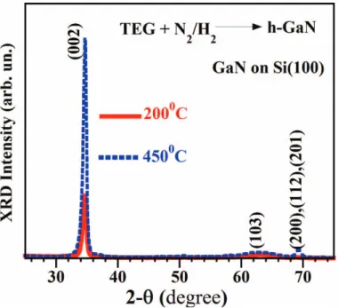
GIXRD analysis revealed hexagonal phase with the most dominant reflection as (002) and a shoulder (103) reflection from GaN samples grown with HCPA-ALD irrespective of substrate temperature. Another peak, which encloses the (200), (201), and (112) reflections from hexagonal GaN phase was also observed. No other phase mixing was detected (i-e cubic). Peak intensity showed a significant increase with increase in growth temperature. More intense peaks obtained at higher growth temperature (450 °C) indicates crystallinity enhancement due to faster reactions and mass transport kinetics. The decreased full width half maximum (FWHM) also indicates an increase in average crystallite size of the GaN grown at higher temperature (450 °C) in comparison with low temperature (200 °C) grown GaN. XPS measurements from GaN films revealed no carbon from the bulk of the film which showed effective removal of carbon ligands during the reaction between Ga source precursor (TEG) and nitrogen source precursor (N2/H2 plasma). 3.24 and 1.71 at. % oxygen
was detected from the GaN films grown at 200 and 450 °C, respectively. With the increase in growth temperature, HR-XPS scans (not shown here) obtained from bulk of GaN showed a shift in Ga 3d and N 1s binding energies from lower to higher energy values. This change was attributed to variation in band bending due to reduction in oxygen impurities of GaN structure with increase in temperature.
AFM measurements revealed Rms surface roughness value of the films grown at 200 and 450 °C as 0.36 and 0.98 nm, respectively. Film deposited in self-limiting growth regime (200 °C) exhibited relatively smooth morphology in comparison with film grown at higher temperature (450 °C).
Ellipsometer measurements were carried out to reveal refractive index, extinction coefficient, and band gap information of the films. Refractive index was found as 2.18 and 2.38 for the films grown at 200 and 450 °C. Strong temperature dependence of the refractive index might be due to variation in surface morphology and improvement in crystallinity with increase in temperature. Refractive index obtained from both the films grown at different temperature matches well with the refractive index of poly crystalline GaN films. Optical band gap value obtained from evaluation of absorption coefficient data revealed the band gap of the films as 3.60 and 3.52 for films grown at 200 and 450 °C, respectively. On the other hand, fitting of optical transmission data with model dielectric function revealed optical band gap as 3.55 and 3.50 for films grown at 200 and 450 °C. Nevertheless, optical band gap information extracted from ellipsometer data analysis and modeling of transmission data is higher than the band gap value of bulk GaN (3.4 eV). This increase was attributed to crystal disorder, grain boundary misorientations, and dislocations.
Fig. 1. (Color online) GIXRD patterns of GaN films grown at two different substrate temperatures.
B. Effect of Ga source precursor
Effect of precursor pulse lengths on growth rate was investigated in order to optimize the process. Ellipsometer measurements revealed that growth rate was saturated for 0.03 and 0.5 s of TMG and TEG pulse lengths respectively. This indicates that all the reactive sites get occupied at these specific pulse lengths of the gallium precursors and growth becomes self-limiting which is a hall mark of ALD. The difference in GPC might come from various possible physical and chemical properties of the precursors i-e (vapour pressure, steric hindrance effect, nucleation behavior, and sticking coefficient)
GIXRD measurements were conducted to obtain the crystallographic information from the GaN grown by two different precursors. For both the samples, GaN (002) and
h-2016 IEEE 36th International Conference on Electronics and Nanotechnology (ELNANO)
134 GaN (103) peaks were observed. Slightly less FWHM and higher peak intensity was observed for GaN grown using TMG indicating better crystalline quality. AFM images showed that TMG grown GaN possesses larger grains (21.2 nm) which results in higher roughness as compare to TEG grown GaN which shows relatively smaller grain sizes (5.6 nm).
Fig. 2. (Color online) GIXRD patterns of GaN thin films grown with TMG and TEG on Si (100) at 200 °C
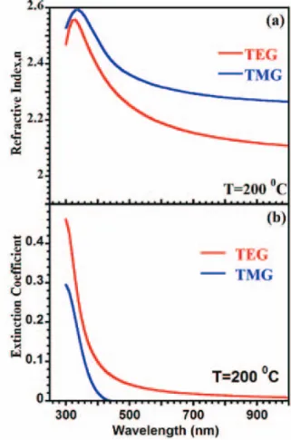
Refractive index, extinction coefficient, and optical band edge values were evaluated from spectroscopic ellipsometer measurements. Refractive index value was found as 2.31 and 2.18 for TMG and TEG grown GaN samples, respectively (Fig. 3a). It is an interesting observation that GaN grown by TEG reveal considerably higher value of refractive index as compare to TEG grown GaN. Both values from TEG and TMG grown GaN are matching well with the reported refractive index value of polycrystalline GaN. Higher value of refractive index obtained from TMG grown GaN is attributed to larger grain size and improved crystallinity as determined from AFM and XRD, respectively. Optical band gap values evaluated for TMG- and TEG-grown GaN are found to be 3.57 and 3.6 eV, respectively. Both these numbers are higher than the value of 3.43 eV for bulk single crystalline GaN, which was speculated to be due to polycrystallinity and presence of multiple oriented crystallites.
CONCLUSION
Here we have reviewed our recent efforts on growing GaN thin films with HCPA-ALD at two different substrate temperatures (200 and 450 °C) and with two different Ga source precursors (TMG and TEG). We have compared structural, chemical, and optical properties of GaN grown at different conditions as mentioned above. The increase in the substrate temperature yields an increased growth rate, larger crystallite size, higher surface roughness, lower optical band gap value, and higher refractive index. Based on higher crystallinity, higher grain size, and higher refractive index obtained for TMG
grown GaN, we argued that TMG might be a better gallium source for HCPA-ALD at low substrate temperatures.
ACKNOWLEDGMENTS
This work was performed at UNAM institute of material science and nanotechnology. M.A. acknowledges the financial support from TUBITAK Grant No. 114F002 and Marmara University BAPKO Project Nos. FEN-A-110913-0378 and FEN-D-130515- 0201. N.B. acknowledges financial support from TUBITAK Grant Nos. 112M482 and 214M015.
Fig. 3. (Color online) (a) Refractive index and (b) extinction coefficient plotted against wavelength for GaN films grown using TMG and TEG.
REFERENCES [1] R.L. Puurunen, J. Appl. Phys., 2005, 97, 121301.
[2] H. B. Profijt, S. E. Potts, M. C. M. van de Sanden, and W. M. M. Kessels, J. Vac. Sci. Technol. A 29, 050801 (2011).
[3] A. Haider, S. Kizir, C. Ozgit-Akgun, E. Goldenberg, S. A. Leghari, A. K. Okyay, and N. Biyikli, J. Mater. Chem. C 3, 9620 (2015).\
[4] M. Alevli, N. Gungor, A. Haider, S. Kizir, S. A. Leghari, and N. Biyikli, J. Vac. Sci. Technol. A 34, 01A125 (2016).
[5] P. Motamedi and K. Cadien, RSC Adv. 5, 57865 (2015).
[6] K. E. C. M. Krishnan, R. G. Jahn, W. F. von Jaskowsky, AIAA J. 15, 1217 (1977).
[7] M. Alevli, A. Haider, S. Kizir, S. A. Leghari, and N. Biyikli, J. Vac. Sci. Technol. A 34, 01A137 (2016).