Low Power UWB Transceiver Design Using Dynamic Voltage Scaling
Rajesh Garg
Texas A&M University College Station, TX, USA
Chunjie Duan, Jinyun Zhang
Mitsubishi Electric Research Labs Cambridge, MA, USA
{duan,jzhang}@merl.com
Sinan Gezici
Bilkent University
Dept. of Electrical & Electronics Eng. TR-06800 Bilkent, Ankara, TURKEY
Abstract—Low power consumption is a critical issue in many
UWB systems. In this paper, we investigate the application of dynamic voltage scaling (DVS) and other low power design techniques to a multiband-OFDM UWB transceiver baseband circuit design in order to reduce average power consumption of the chip. Our results show significant power savings over the conventional approach.
Keywords-Ultra-wideband; multiband OFDM; dynamic voltage scaling; low power circuit design; Viterbi decoder.
I. INTRODUCTION
In February 2002, the Federal Communication Commission (FCC) of the US issued a report that allows limited unlicensed operation of ultra-wideband (UWB) devices [1]. This accelerated the already intense research and development of the UWB technologies and UWB-based systems [2], [3]. UWB has since been agreed to be a viable solution for high speed personal area network (PAN) and other wireless applications where high data rate is desired. Many other countries have now allocated the spectrum for UWB systems, or are in the process of doing so.
Among all the competing UWB technologies, the multi-band orthogonal frequency division multiplexing (MB-OFDM) based system is the most mature and promising technology that offers high throughput and robustness [3]. In 2005, Ecma Internal released the UWB standard based on WiMedia1 UWB platform [4].
Many companies are now offering MB-OFDM UWB products. However, most of the commercially available products on the market have relatively high power consumption. Such high power consumption often imposes a limitation on the use of UWB for applications where low power is desired, or sometimes required.
This paper discusses the techniques for minimizing the power consumption of the baseband circuit of a MB-OFDM UWB transceiver. We focus on architecture and operation of the MB-OFDM UWB transceiver and propose a packet based dynamic voltage scaling (DVS) approach that offers significant power savings over the conventional design.
The remainder of the paper is organized as follows. Section II examines some basics of the MB-OFDM UWB physical layer, where we focus on the packet structure which is directly related to the operation of the individual components of the transceiver. Section III reviews the DVS technique and shows how it can lower the average power of the UWB transceiver. Section IV provides detailed discussion on how to realize a
high speed and low power implementation for one of the key components in the UWB transceiver; namely, the Viterbi decoder. Experimental results are given in Section V, and some conclusions are made in Section VI.
II. MB-OFDM UWB PHYSICAL LAYER
Although the MAC and higher layers significantly affect the overall power consumption of the system, they generally have little impact on the design of the hardware system. The physical layer specification, however, is directly related to the operation of the hardware and needs to be fully comprehended in order to achieve a hardware design with optimal power consumption. This section gives a brief description of some of the main features of the MB-OFDM PHY specifications.
A. Basic Principles and Signal Structure
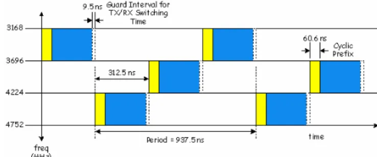
The UWB transmission is packet based. Each UWB packet is an assembly of OFDM symbols, each of which consists of 128 tones (with a spacing of 4.125 MHz) and occupies a 528 MHz bandwidth. Out of 128 tones, there are 100 data tones that carry information, 10 pilot tones for carrier recovery, 12 guard tones and 6 null tones to ease the filter roll-off specification. In the time domain, at 528 Ms/s, each symbol consists of 160 sample points with the first 128 samples being the data samples followed by 32 zero-padded samples. The zero padding is to mitigate the effects of inter-symbol interference (ISI) and to allow the receiver to perform add-back for collecting sufficient symbol energy. Also, a 5-sample (~9.5 ns) guard interval is inserted between symbols to allow RF band switching.
The average transmitter power density is -41.3 dBm/MHz according to the FCC regulations. The system operates in the 3.1-10.6 GHz band, hopping over 3 or 7 sub-bands. In each sub-band, OFDM symbols with a bandwidth of 528 MHz are transmitted. The transmitter and receiver do not operate at the same time and therefore the link can be considered half duplex.
Figure 1 illustrates a 3 sub-band hopping operation. The symbols are transmitted over one of the 3 RF sub-bands. For packets with data rates lower than or equal to 80 Mb/s, the frequency domain spreading (FDS) is enabled. In other words, each information symbol is transmitted on two separate tones within an OFDM symbol. This added diversity improves the link performance. Also, the time domain spreading (TDS) is employed for data rate options lower than or equal to 200 Mb/s, which involves transmitting the same information across two consecutive OFDM symbols.
B. Transceiver Architecture
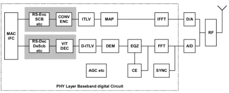
UWB transceiver hardware typically has the RF front end and the baseband circuit as shown in Figure 2. They can be implemented either in a chip set or as a single CMOS chip.
RF D/A A/D IFFT FFT SYNC MAP ITLV D-ITLV CONV ENC RS-Enc SCB etc CE EQZ DEM VIT DEC RS-Dec DeScb etc AGC etc
PHY Layer Baseband digital Circuit MAC
IFC
Figure 2. UWB transceiver functional blocks
The RF subsystem can be further broken down into the transmitter and the receiver. The transmitter up-converts the baseband I/Q signals to RF signal, and typically consists of quadrature modulator, hopping band control, amplifiers and necessary filters. The receiver circuit down-converts the received signal to baseband I/Q signals and consists of LNA, quadrature demodulator, automatic gain control (AGC) and phase lock loop or frequency tracking. Since the focus of this paper is on the baseband circuit design, we will not go into details of the RF circuitry.
The A/D and D/A converters bridge the digital section and the RF front end. Both the D/A and A/D converters have the sample rate of 528 MHz, which is the Nyquist frequency of the baseband signals.
The major functional blocks in the baseband logic shown in Figure 2 are:
• FFT/IFFT: It should be noted that even though separate FFT and IFFT are shown in the figure, in practice only a single FFT/IFFT engine is implemented and shared by the transmitter and receiver. The engine performs transformation between 128 tones in the frequency domain and 128-samples in the time domain.
• Synchronization (SYNC) block locates the start of the packet by detecting the synchronization symbols in the preamble section of the packet. It triggers the operation of the rest of the receiver blocks.
• Constellation mapping (MAP) maps 100 or 200 data bits into 100 tones depends on the packet data rate. It also inserts pilot and guard tones into the symbol. • The demodulation block (DEM) performs the inverse
of the MAP block. 100 or 200 data bits are retrieved from every FFT ouput depending on the packet data rate.
• Channel estimation (CE) and equalization (EQZ) blocks perform equalization on each received symbol to facilitate mapping of the data into the correct constellations.
• The convolutional encoder (CONV-ENC) block encodes the data into a convolutional code with a constraint length of 7 and code rate varies from 1/3 to 3/4. It has a 1/3 convolutional encoder followed by a puncturer that has variable puncturing rate depending on the packet data rate.
• The Viterbi decoder (VIT-DEC) decodes the data bits from the received symbols. More detailed discussion is given in the Section IV.
• Automatic gain control (AGC) controls the gain in the RF front end. Some transceivers have TX power control which is not shown in the figure.
• The carrier frequency offset tracking and compensation is implemented either entirely in digital domain or with a combination of digital and analog circuitry.
• Other functional blocks not listed individually are (de)interleaver ((D)-ITLV), Reed Solomon encoder and decoder (RS-ENC and RS-DEC), scrambling (SCB), descrambling (DeSCB), data packet buffer and interface logic to MAC layer.
Note that various functional blocks run at different speeds, and consume different amounts of power. Some blocks are only active during the preamble section, while others are turned on only for data. To optimize the total power consumption, we need to understand the packet structure since it is directly related to the operation of each block.
C. Packet Structure
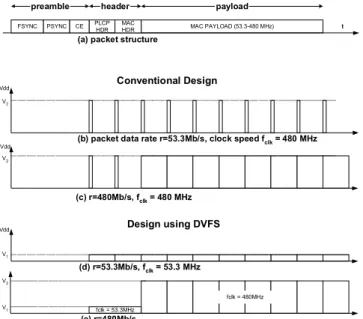
The structure of a UWB packet is shown in Figure 3(a). The packet can be divided into three sections: preamble, header and payload. Each section consists of symbols as discussed before.
The preamble section has 30 symbols. All the symbols are predetermined: frame sync (FSYNC), packet sync (PSYNC) and channel estimation (CE) symbols. FSYNC and PSYNC symbols are used by the synchronization circuit in the receiver to determine the start of the packets. CE symbols are only used by the channel estimation.
The header data include PLCP field and MAC header field. Some of the PHY layer parameters such as data rate, scrambler seed and packet size are embedded in the PLCP field. MAC header contains information for the MAC layer operation; but
from the PHY layer standpoint, it is treated the same as the MAC payload. The header section contains 12 symbols and is always coded at 53.3 Mb/s.
The payload section can have up to 492 symbols. The data rate for the payload ranges from 53.3 Mb/s up to 480 Mb/s.
The SYNC block is active before and during the FSYNC and PSYNC period. During this period, other blocks are inactive. Similarly, the CE block is active for the duration of 6 CE symbols. Other blocks are not active during this period.
Other receiver blocks start operation in the default mode (53.3 Mb/s) after the CE symbols. The packet data rate is retrieved from the PLCP field, and at the end of the header section, the data rate is switched.
MAC PAYLOAD (53.3-480 MHz) PLCP HDR t fclk = 53.3MHz Vdd Vdd Vdd V1 V1 V2 fclk = 480MHz
(a) packet structure
V2
V2
FSYNC PSYNC CE MAC HDR
(b) packet data rate r=53.3Mb/s, clock speed fclk = 480 MHz
(c) r=480Mb/s, fclk = 480 MHz
(e) r=480Mb/s
(d) r=53.3Mb/s, fclk = 53.3 MHz
Design using DVFS Conventional Design
preamble header payload
Figure 3. Packet structure and data rate
D. Data Rate Dependency
The data rates supported in the Ecma MB-OFDM UWB standard range from 53.3 Mbps to 480 Mbps. Depending on the channel condition or the throughput requirement of the applications, the UWB link can operate at one of the rates listed in Table 1.
The variable data rate is achieved by TDS, FDS, or by changing the code rate (through puncturing), as listed in Table 1.
Table 1. PSDU rate dependent parameters Data rate (Mb/s) Modulation TDS FDS Code rate Bits
/6Syma Info Bits
/6Symb 53.3 QPSK Y Y 1/3 300 100 80 QPSK Y Y 1/2 300 150 106.7 QPSK Y N 1/3 600 200 160 QPSK Y N 1/2 600 300 200 QPSK Y N 5/8 600 375 320 DCM N N 1/2 1200 600 400 DCM N N 5/8 1200 750 480 DCM N N 3/4 1200 900 a. Before de-depuncturing b. After de-puncturing
Some of the functional blocks in Figure 2 such as FFT/IFFT, SYNC and CE, always operate at the sample rate of 528 MHz. Other blocks, however, have different input rates. The input rates to the blocks in the shaded area vary depending on the data rate of the transmitted or the received packets. This important observation facilitates voltage/frequency scaling approach as will be discussed in the following sections.
III. VOLTAGE SCALING IN LOW POWER CIRCUIT DESIGN The power consumption of a CMOS circuit is given by the following equation [6]: leak dd dd eff total
C
V
f
V
I
P
=
⋅
2⋅
+
⋅
(1) where Ceff is the gate capacitance, Vdd is the supply voltage, Ileakis the leakage current, and f is the switching frequency.
The first term in (1) is called dynamic power (Pdyn). It is
zero when there is no transition at the gates. The second term is the leakage power Pleak, which is always non-zero as long as
power is applied to the circuit. Traditionally, Pdyn >> Pleak is
true, and Pleak is negligible for Ptotal estimation. However, this
does not hold true any more for deep sub-micron (DSM) processes. The shrinking gate size causes Pdyn to decrease, but
at the same time increases Pleak. In some designs, Pleak can
exceed Pdyn.
As indicated in equation (1), lowering Vdd reduces both Pdyn
and Pleak. Therefore, it is obvious that lowering Vdd will yield
lower power. Unfortunately, scaling down Vdd also increases
the delay of the circuit since CMOS gate delay is a function of
Vdd as given by the following equation [16]:
α
τ
)
(
dd T dd LV
V
V
C
k
−
⋅
⋅
=
(2)where
k
is associated with the drivability factor and can be considered a constant, CL is the load capacitance and α is aprocess dependent parameter that generally ranges between 1.5 and 4, and VT is the threshold voltage, which is also process
dependent. As Vdd approaches VT, the delay τ increases.
Therefore, the voltage can only be scaled down so long as the timing closure is still met.
A conventional design using fixed supply voltage must meet the tightest speed requirements. When the input data is not always at the maximum rate, additional signals are used to throttle the circuit. An example is given in Figure 3(b) and 3(c). The circuit (e.g., the Viterbi decoder in a UWB receiver) is designed to operate at a fixed Vdd =V2 and a clock frequency of
fclk=480 MHz. The maximum throughput is 480 Mb/s. In case
of a received packet with lower data rate, valid data is present at the input only for a fraction of the total period. The duty cycle of the valid data (ρ) is determined by the ratio of the actual data rate and the maximum data rate the circuit handles. Figure 3(b) shows the supply voltage level when a packet with a data rate of 53.3 Mb/s is received. Figure 3(c) shows the case
for a packet with data rate of 480 Mb/s. In both cases, the average power consumption can be expressed as:
)
1
(
ρ
ρ
+
⋅
−
⋅
=
active leakage averageP
P
P
(3)The dynamic voltage scaling (DVS) exploits the fact that a lot of times a circuit can run at a lower speed and yet still be able to process the data in time [15]. By scaling down Vdd, the
average power can be lowered. Since the voltage scaling is generally associated with frequency scaling, sometimes it is referred to as dynamic voltage and frequency scaling (DVFS). DVFS has been used in some low power, real time embedded systems. The scheduler (normally a piece of software in the operating system) computes the clock speed needed for a particular task based on the deadlines and scale the voltage and clock frequency accordingly.
It can be observed from the packet structure that it is feasible to use DVS in the MB-OFDM transceiver design. Figure 3(d) shows the case when data at a rate of r=53.3Mb/s is received. Since both the header and payload sections have the same data rate, only a single voltage Vdd =V1 is needed. If a
480Mb/s packet is received as shown in Figure 3(e), Vdd =V1 is
applied during the header section. For the payload section, a different voltage Vdd =V2 is used. The clock frequency is
adjusted accordingly.
A hardware scheduler is needed to implement DVS. The scheduler is a very simple circuit controlled by the SYNC block and the packet data rate.
IV. CASE STUDY: UWB VITERBI DECODER
To understand how to implement a DVS-enabled UWB transceiver, we use the Viterbi decoder as a case study. The Viterbi decoder used in the UWB transceiver a) handles the variable data rate and b) by estimation consumes almost 30% of the total power, and therefore is a good candidate to illustrate the benefits of DVS.
The Viterbi algorithm is a maximum likelihood decoding procedure for convolutional codes [8]. Its effectiveness in decoding convolutional codes has made it a key block for most of the modern communication systems where convolutional coding is used.
The complexity and speed of the Viterbi decoder is directly related to several parameters: code rate R, constraint length K and the number of soft input bits.
There have been a lot of studies on the efficient implementation of the Viterbi decoder. Some focus on high speed, some on power consumption and others on coding gain, etc [5], [7]. The convolutional code defined in the Ecma UWB system has R=1/3 and K=7. In order to achieve the desired system performance, 3 (or sometimes more) soft input bits are used.
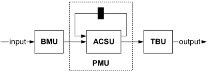
Most of the Viterbi decoder implementations typically include three blocks: Branch metric unit (BMU), add-compare-select unit (ACSU) and trace-back unit (TBU).
The BMU's function is to calculate branch metrics, which are distance metrics between every possible symbol in the code
alphabet, and the received symbol. The number of soft input bits determines the complexity of the BMU. There need to be 2K BMUs in the decoder. The BMU implementation is the most
straightforward among these blocks and normally can run at high speed. The BMU contributes little to the overall power consumption of the decoder.
The path metric unit (PMU) summarizes branch metrics to obtain the metrics for 2K − 1 paths, one of which can eventually
be chosen as the optimal one. At every clock cycle, it makes 2K−1 decisions, throwing away wittingly non-optimal paths. The
results of these decisions are written to the TBU.
The ACSU is the main component inside the PMU and normally is the speed bottleneck because of the recursive operation [9]. The output needs to be valid before the next input and therefore the computation must be completed in one clock cycle.
There are generally two types of implementation for ACSU: radix2 and high index [10]-[12]. The radix2 design handles one symbol per clock and therefore needs to run at the data rate. For some very high data rate applications where the speed requirement is difficult to meet, high index can be used. Such a design processes m bits per clock, and therefore only needs to operate at 1/mth of the data rate. It is often referred to as the radix (2m). However, the overall circuit complexity for a
high index design grows exponentially. In practice, it is rare to use higher than radix4 implementation.
The PMU is typically the most power consuming block in a decoder because of the complexity. There are 2k-1 ACSUs in a
radix2 implementation. Again, this number grows when a higher index is used.
The TBU restores an (almost) maximum-likelihood path from the decisions made by the PMU. Since the path is restored in inverse direction, a Viterbi decoder comprises a FILO (first-in-last-out) buffer to reconstruct a correct order.
The complexity of the TBU is directly related to the trace-back length. Theoretically, to achieve the maximum coding gain, the Viterbi decoder needs to start the trace back from final state. This implies large amount of memory needed to implement the decoder, which significantly increases the latency of the decoder. In practice, the trace-back length is limited to 5 times the constrain length. In our case where K=5, a minimum of 35 states are needed for a path originated from each state.
BMU ACSU TBU
input output
PMU
It should be noted that although the de-puncturing sometimes is considered as a part of the Viterbi decoder, we moved it outside of the Viterbi decoder since it is part of the path that generates variable rate input data to the Viterbi decoder. Since the input and output of the de-puncturer have different rates, some form of buffering must be used.
Our target is to compare the speed and the power consumption of the Viterbi decoder designs in a conventional implementation (fixed voltage) and a DVS-enabled implementation.
The designs implement standard MB-OFDM UWB code (R=3 and K=7), use 3 soft input bits and are designed to handle at least 480 Mb/s.
In the conventional implementations, we hold the input values when no valid data are present along with the data valid signal to halt the internal circuit. Both Pdyn and Pleak are
included in the calculation of the total power. The results are presented in the next section.
V. EXPERIMENTAL RESULTS
In this section, we perform simulations using SPICE in order to investigate the efficiency of the DVS approach. All of our SPICE models are built using a generic BSIM3 0.1µm process.
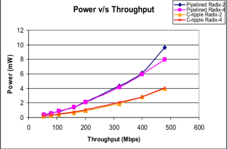
We compare radix2 and radix4 implementations for an ACSU using pipelined [14] and carry-ripple [13] structures. The simulation results in Figure 5 indicate that, at the same throughput, the pipelined versions consume more power than the carry-ripple implementations for both radix2 and radix4. It is also observed that the difference between radix2 and radix4 is very small. This is because even though the radix4 is a lot more complicated (more gates) than the radix2 implementation, the circuit for radix4 is running at only half the speed. The difference becomes noticeable only for the pipelined structure at 480 Mb/s, where the radix4 has lower power than the radix2. Therefore, for high speed decoders with pipelining, radix4 can have some power savings compared to radix2, which is, however, not significant enough to justify the use of complex radix4 structure. Therefore, radix2 is chosen for its simplicity and small size.
Power v/s Throughput 0 2 4 6 8 10 12 0 100 200 300 400 500 600 Throughput (Mbps) Po w e r ( m W ) Pipelined Radix-2 Pipelined Radix-4 C-ripple Radix-2 C-ripple Radix-4
Figure 5. Throughput vs. power for various ACSUs
Similarly, we perform SPICE simulations for the TBU. The same relation between throughput and power is observed, as shown in Figure 6. Trace-Back Unit 0 0.2 0.4 0.6 0.8 1 1.2 1.4 0 100 200 300 400 500 600 Throughput (Mbps) Po w e r ( m W )
Figure 6. Throughput vs. power for a TBU
Table 2 lists power consumption for various supply voltages for all the data rates specified in the MB-OFDM UWB standard. The numbers for the conventional design is also listed in the table (the last row). We also define a parameter, Energy/Mb, which is the energy consumed for decoding one million bits. As the table shows, simply by lowering the supply voltage (static voltage scaling), we are able to achieve 4 times the power saving. The additional 2-3 times power savings can be obtained by using DVS.
Table 2. Power and energy per bit vs. supply voltage for various data rates Pipe-lined ACSU Carry ripple ACSU Data
Rate
(Mb/s) Voltage
(V) Power (mW) Energy/Mb (mJ) Voltage (V) Power (mW) Energy/Mb(mJ) 53.3 0.38 0.34 0.0063 0.41 0.18 0.0035 80 0.42 0.61 0.0076 0.42 0.29 0.0036 106.7 0.43 0.86 0.0080 0.43 0.40 0.0038 160 0.45 1.43 0.0089 0.46 0.67 0.0042 200 0.5 2.17 0.0108 0.50 0.94 0.0047 320 0.56 4.33 0.0135 0.55 1.89 0.0059 400 0.60 6.13 0.0153 0.6 2.84 0.0071 480 0.69 9.62 0.0200 0.65 4.00 0.0083 480 1.2 33.3 0.0694 1.2 15.7 0.0328
As can be observed from the table, the supply voltages for some data rates are very close. Therefore, it is possible to group some rates together and therefore to reduce the numbers of
voltages and clock frequency in order to simplify the system design. An example is shown in the table by means of different color codes for different groups.
Table 2 can also be used to select a fixed Vdd on
transceivers that support a maximum data rate other than 480 Mb/s. For example, if a node needs to support only 110Mb/s, a single fixed 0.43 V can be used.
VI. CONCLUSIONS
WiMedia’s PHY layer specification calls for variable data rate. This allows the UWB link to adapt to various channel conditions and application throughput requirements. Our study has shown that it is feasible to employ DVS in the transceiver design to achieve low average power consumption. We have used the Viterbi decoder as an example to demonstrate the power savings through this design technique. For each individual component inside the Viterbi decoder, we have compared the speed, power consumption and chosen the implementation that meets the speed requirement and yet yields the minimum power consumption and/or area. Our SPICE simulations have shown that by applying DVS, one can achieve significant power savings.
ACKNOWLEDGMENT
This work is funded by Renesas Technology Inc. REFERENCES
[1] U. S. Federal Communications Commission, FCC 02-48: First Report and Order, Feb. 2002.
[2] P. Runkle, J. McCorkle, T. Miller and M. Welborn, “DS-CDMA: the modulation technology of choice for UWB communications,” IEEE
Conference on Ultra Wideband Systems and Technologies, pp. 364-368,
Batimore, MD, Nov. 16-19, 2003.
[3] E. Saberinia and A. H. Tewfik, “Multi-user UWB-OFDM communications,” IEEE Pacific Rim Conference on Communications,
Computers and Signal Processing (PACRIM 2003), vol. 1, pp. 127-130,
Victoria, Canada, Aug. 28-30, 2003.
[4] ECMA-368, “High rate ultra wideband PHY and MAC standard,” 1st edition, Dec. 2005, [Online]. Available: http://www.ecma-international.org/publications/files/ECMA-T/ECMA-368.pdf
[5] W.-S. Ju, M.-D. Shieh and M.-H. Sheu, “A low power VLSI architecture for the Viterbi decoder”, Proc. 40th Midwest Symposium on Circuits and
Systems, vol. 2, pp. 1201-1204, Aug. 1997.
[6] A. Chandrakashan and R. Brodersen, Low Power CMOS Design, Wiley-IEEE Press, Feb. 1998.
[7] J. Tang and K. K. Parhi, “Viterbi decoder for high-speed ultra-wideband communication systems”, Proc. ICASSP 2005, vol. 5, pp. 37-40, March 2005.
[8] Andrew J. Viterbi, “Error bounds for convolutional codes and an asymptotically optimum decoding algorithm”, , IEEE Transactions on
Information Theory 13(2):260–269, April 1967.
[9] S.-W. Choi and S.-S. Choi, “200Mbps Viterbi decoder for UWB,” Proc.
7th International Conference on Advanced Communication Technology (ICACT 2005), vol. 2, pp. 904-907, Feb. 2005.
[10] G. Fettweis and H. Meyr, “High-rate Viterbi processor: A systolic array solution,” IEEE Journal on Selected Areas in Communications, vol. 8, no. 8, pp. 1520-1534, Oct. 1990.
[11] H. F. Lin and D. G. Messerschmitt, “Algorithms and architectures for concurrent Viterbi decoding,” Proc. IEEE International Conference on
Communications (ICC 1989), vol. 2, pp. 836-840, June 1989.
[12] P. J. Black and T. H.-Y. Meng, “A 140-Mb/s, 32-state, radix-4 Viterbi decoder,” IEEE Journal of Solid-State Circuits, vol. 27, issue 12, pp. 1877-1885, Dec. 1992.
[13] M Anders et al. “A 64-state 2GHz 500 Mbps 40mW Viterbi accelarator in 90nm CMOS”, IEEE Symposium on VLSI Circuit Digest of Technical
Papers, 2004.
[14] K. K. Parhi, “Novel pipelining of MSB-first add-compare select unit structure for Viterbi decoders,”, IEEE International Symposium on
Circuits and Systems, vol. 2, pp. 501-504, May 2004.
[15] R. Gonzalez, B. Gordon, M. Horowitz, “Supply and threshold voltage scaling for low power CMOS,” IEEE J. of Solid-State Circuits, vol. 32, Aug. 1997.
[16] T. Sakurai and A. R. Newton, “Alpha-power law MOSFET model and its applications to CMOS inverter delay and other formulas”, IEEE J. of