Local Reconstructions of Silicene Induced by Adatoms
V. Ongun Özçelik
†,‡and S. Ciraci*
,†,‡,§†UNAM-National Nanotechnology Research Center, Bilkent University, 06800 Ankara, Turkey ‡Institute of Materials Science and Nanotechnology, Bilkent University, Ankara 06800, Turkey §Department of Physics, Bilkent University, Ankara 06800, Turkey
ABSTRACT: The interaction of silicene with Si, C, H, O, and Ti atoms along with H2, H2O, and O2molecules are investigated and
the induced functionalities thereof are analyzed using first principles density functional theory. Si adatom initially adsorbed at the top site of silicene pushes down the Si atom underneath to form a dumbbell like structure with 3 + 1 coordination. This prediction is important for silicene research and reveals new physical phenomena related to the formation of multilayer Si, which is apparently the precursor state for the missing layered structure of silicon. We found that dumbbell structure attributes coverage-dependent electronic and magnetic properties to non-magnetic bare silicene. Even more interesting is that silicene with
dumbbells is energetically more favorable than the pristine silicene: The more dense the dumbbell coverage, the stronger is the cohesion. Incidentally, these structures appear to be intermediate between between silicene and silicon. The carbon adatom, which is initially adsorbed to the bridge position, substitutes one Si atom, if it overcomes a small energy barrier. The oxygen molecule can dissociate on the silicene surface, whereby constituent oxygen atoms oxidize silicene by forming strong bonds. By varying the concentration and decoration of carbon, hydrogen and oxygen atoms, one can tune the band gap of silicene. Through the adsorption of hydrogen or titanium adatom, silicene acquires spin-polarized state. A half-metallic ferromagnetic behavior is attained at specific uniform coverage of Ti adatom, which may function as a spin valve.
■
INTRODUCTIONJust after the synthesis of quasi 1D tubular1,2 and 2D single layer graphene3,4structures, which have exhibited exceptional properties, answers to the critical question of whether Si can form similar structures have been desperately sought.5−7This question was rather logical, because C and Si are group IV elements of the periodic table and hence they are isovalent. Also it has been attempted to adopt the technology developed behind the Si crystal to Si nanostructures. Unfortunately, the attempts of searching single layer Si in honeycomb structure have been discouraged usually by the arguments that Si does not have a layered allotrope like graphite. Surprisingly, free-standing silicene and germanene, namely graphene-like single layer honeycomb structures of silicon and germanium, have been shown to be stable.8Also it has been shown that silicene shares several of the exceptional properties of graphene, such as the linearly crossing ofπ- and π*-bands at the Fermi level (if a very small gap opening of ∼1 meV due to the spin−orbit coupling is neglected),9 the ambipolar effect and the family behavior observed in nanoribbons.10Although the strongπ−π coupling ensures a planar geometry of graphene, this coupling weakens in silicene. However, the endangered stability is regained by the rehybridization of 3s and 3p valence orbitals to 4-fold sp3-like bonds through the dehybridization of 3-fold planar sp2 bonds. This leads to the buckling of the planar
honeycomb structure. Accordingly,a single atomic plane of graphene is replaced by two atomic planes, which are split by a
buckling of Δ = 0.44 Å and the alternating Si atoms at the corners of the hexagons are located in different atomic planes. Owing to the buckling (or puckering) of the structure, the vertical symmetry can be broken under a perpendicular electric field, which polarizes the Si atoms and hence opens a band gap.11−14Presently, silicene has been an activefield of research with several challenges.15−20 Searches on the similar single layer, honeycomb topology have extended to group IV−IV, III−V, and II−VI compounds7,21−23 including SiC24 and ZnO,25,26 as well as transition metal oxides and dichalcoge-nides.27,28 Each of these structures has been predicted to display interesting properties with potential applications in nanotechnology. Nowadays, great expectations for fundamental properties and technological application have been directed toward various single layer nanostructures and their composite, van der Waals thinfilms.29
Our earlier predictions7,8,10on the stability of silicene and its properties have been confirmed recently by realizing the growth and characterization of single layer silicene on the Ag substrate.30,31 These studies, at the same time, initiated a growing interest in silicene. Even though two-dimensional semimetallic silicene has limited applications for
nano-Received: August 29, 2013
Revised: November 17, 2013
Published: November 25, 2013
electronics, several new functionalities can be achieved by chemisorption of a number of foreign atoms or molecules.32−34 Motivated by the self-organized behavior of carbon host atom on graphene,35−37here we investigate the effects of silicon and carbon adatoms on silicene. The silicon adatom is a host atom and its interaction with silicene may be crucial for the study of the growth of the multilayer silicene. Additionally, the decoration through uniform Si coverage may attribute useful functionalities to silicene. Being a group IV element, the carbon adatom is isovalent to Si and its interaction with silicene is also important for future graphene−silicene composite materials like silicene, including SiC quantum dots. Apart from Si and C adatoms, we also study the interactions of silicene with of H, O, Ti adatoms and H2, H2O, and O2 molecules. Oxygen and
hydrogen atoms are known to form strong bonds on the surface of bulk silicon and are crucial elements in Si-based micro-electronics. In particular, it is important to know whether silicene is oxidized as easily as bulk Si does. Finally, Ti is a 3d-transition metal atom and may form strong bonds with silicene for metallic contacts like Ti on graphene. Therefore, the interaction of these atoms with silicene and the selected functionalities attained thereof have been the focus of this work. Our study is based on free-standing (suspended) silicene, because it has been shown to be stable8like graphene. Even if silicene is grown on Ag(111) and hence its states engage in hybridization with those of Ag(111) inducing some changes in specific states, the effects of hybridization cease at the top surface of multiple silicene layers. In this respect, our study is relevant for the strong interaction between Si, C, O, H, and Ti adatoms and the silicene surface.
We show that the interactions between the Si adatom and silicene are complex and lead to amazing results, which are of crucial importance in the rapidly developing research on silicene: The silicon adatom on silicene pushes the Si atom underneath and readily forms a dumbbell (D) structure by donating significant electronic charge to the nearest Si atoms. By engaging in a 3 + 1 coordination, D decorated silicene is a structure between the 4-fold coordinated diamond structure and the single layer, buckled silicene. Hence, silicene with dumbbells is slightly more favorable than pristine silicene. The cohesion of uniform D + silicene structure becomes even more superior to that of silicene when the smallest D−D distance, dD−D, is less than√3a (a being the lattice constant of pristine
silicene). Dumbbells also display interesting dynamics and structural transformations, which are crucial for the under-standing of the growth of multilayer silicene. Additionally, we also present the coverage-dependent features of the D + silicene structure.
The carbon adatom also creates unique reconstructions in silicene. Carbon initially forms a bond on the bridge site; however, if a small barrier is passed, the C adatom substitutes one of the host silicene atoms to form a substitutional impurity. On the other hand, the oxygen molecule can dissociate on silicene, where constituent oxygen atoms form strong bonds to oxidize silicene. A bridge-bonded O adatom can pass from the top side to the bottom side of silicene once a small energy barrier is overcome and thus it can easily penetrate across silicene layers. H and Ti adatoms attribute magnetic properties. Silicene acquires integer magnetic moment and half-metallic character due to a specific uniform coverage of Ti.
■
METHODWe have performed spin-polarized density functional theory calculations within generalized gradient approximation (GGA) including van der Waals corrections.38 We used projector-augmented wave potentials PAW,39 and the exchange− correlation potential is approximated with Perdew−Burke− Ernzerhof, PBE functional.40
Using the supercell geometry within the periodic boundary conditions, we considered the adatoms as isolated dopants. In large supercells the adatom−adatom coupling is reduced significantly and conditions of the isolated adatom are approximately met. The localized states of dopants appear as flat bands. Very large supercells are not convenient from the computation point of view. Therefore, one has to optimize the supercell size. In the present study, we used 4× 4 supercells of silicene, which correspond to the uniform coverage of one Si adatom per 32 Si host atom, namelyΘ = 1/32. The size of this supercell is tested to be sufficient to minimize the adatom− adatom coupling for the purpose of the present study. On the other hand, results obtained from relatively smaller supercells are taken for the uniform coverage or decoration of adatoms. Hence, in specific cases, we also treated a uniform coverage of Θ > 1/32 to examine the effects of significant couplings between adatoms.
The Brillouin zone was sampled by (11× 11 × 1) k-points in the Monkhorst−Pack scheme where the convergence in energy as a function of the number of k-points was tested. The number of k-points were further increased to (17× 17 × 1) in small supercell calculations. Atomic positions were optimized using the conjugate gradient method, where the total energy and atomic forces were minimized. The energy convergence value between two consecutive steps was chosen as 10−5 eV. A maximum force of 0.002 eV/Å was allowed on each atom. Numerical calculations were carried out using the VASP software.41
The binding energyEb, is calculated from the expression,Eb
=ET[silicene] + ET[A/M]− ET[A/M + silicene], in terms of
the total energies of bare silicene supercell and of free adatom A (=Si, C, H, O, or Ti) or molecule M (M = H2, O2, H2, or H2O) and the structure-optimized total energy of one A or one M adsorbed to each silicene supercell, respectively. All total energies are calculated in the same supercell. In our notation,Eb
> 0 indicates a binding structure. The formation energy, Ef,
takes into account the binding relative to the ground state of A either in bulk crystal or in a molecule. Accordingly, for the case of hydrogen, for example,Ef= −Eb′/2 + Eb, where Eb′ is the
binding energy of H2 relative to hydrogen atom. Normally,
although a process withEf> 0 is favored,Ef< 0 may give rise to
clustering or desorption under specific circumstances. The bonding and effective charge of adatoms are characterized by calculating total charge density of adatom + silicene system,ρT(r). We presented the charge distribution in
terms of isosurfaces and contour plots. We also carried out Mullliken analysis42in terms of atomic orbitals of constituent atoms to obtain their effective charge, Q*, as implemented in the SIESTA package.43The energy landscape of an adatom on silicene is calculated by placing the adatom to 500 different grid points in the hexagon of silicene and performing self-consistent energy minimization calculation for each point. At each grid point, the x and y coordinates of the adatom were kept fixed while itsz coordinate was relaxed to minimize the total energy. The energy at each grid point is designated by a color code.
The fully relaxed, spin-polarized calculations of Ti adatoms are also repeated using the local basis set in the SIESTA package,
resulting in the same magnetic moment obtained by using plane wave basis set.41
Table 1. Characterization of the Case Where a Single Adatom (Si, C, H, O, and Ti) Adsorbed Uniformly to Each (4× 4) Supercell of Silicene (Corresponding to the CoverageΘ = 1/32)a
adatom BS d (Å) Eb(eV, kJ/mol) Ef(eV) EB(eV) Eg(↑↓/↑↑/↓↓)(eV) Q* (e) μ(μB)
Si D 2.39 3.96 (380) −0.75 0.92 0.08/0.43/0.43 0.22 2.0
C S 1.85 5.88 (564) −1.77 1.52 0.19 −0.42 0
H T 1.51 2.12 (203) −0.13 0.26 0.16/0.29/0.24 −0.20 1.0
O B 1.70 6.16 (591) 2.83 0.65 0.21 −0.34 0
Ti TH 2.50 4.14 (397) −3.59 0.22 0.09/0.09/0.15 (HM*) 0.16 2.0
aBS: binding site, where D, S, T, B, and TH represent dumbbell structure, substitution of adatom, top site, bridge site, and between top and hollow
sites, respectively.d: smallest distance between the adatom and the nearest Si atom. Eb: binding energy in eV/unit cell and in kJ/mol.Ef: formation energy.EB: minimum energy barrier in the migration of the adatom.Eg: smallest band gap between spin-unpolarized conduction and valence bands. For spin-polarized systems the gap between spin-up and spin-down/spin-up and spin-up/spin-down and spin-down conduction and valence bands are given.Q*: effective charge on the adatom. μ: total magnetic moment per supercell. *Note that when four Ti adatoms are adsorbed on the (4 × 4) supercell of silicene uniformly, the resulting structure is a half-metal (HM) with ferromagnetic order.
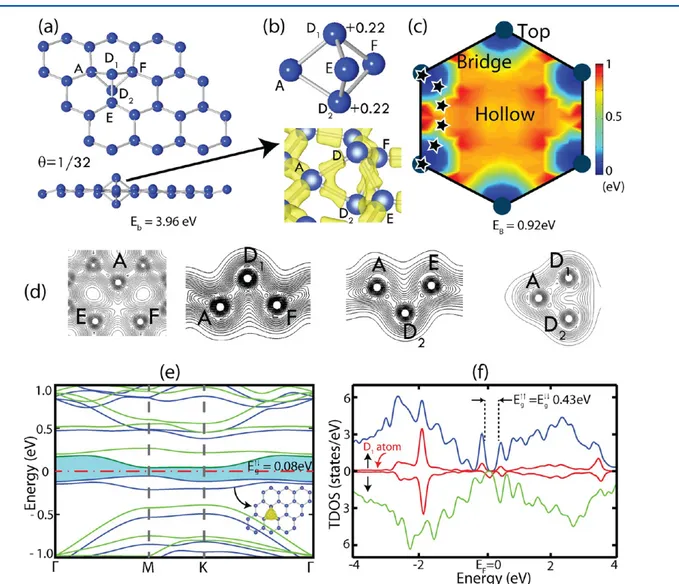
Figure 1.One Si adatom adsorbed to each (4× 4) supercell of silicene, which corresponds to the uniform coverage of Θ = 1/32. (a) Top and side views of the atomic configuration of the dumbbell (D) structure. Blue balls represent Si atoms. (b) Magnified view of the D structure together with the isosurface charge density. D1and D2denote Si atoms at both ends of the dumbbell, and A, E, and F are silicene atoms nearest to D1and D2. Excess charges on the Si atoms of the dumbbell structure are shown by numerals. (c) Energy landscape for the Si adatom on silicene calculated on a hexagon. The migration path of the Si adatom with minimum energy barrierEBis indicated by stars. (d) Contour plot of the total charge density ρT(r), on the horizontal plane passing through A, E, and F atoms, and on the planes passing through A−D1, A−D2, and D1−D2bonds. (e) Energy band structure of the D + silicene structure with the dash-dotted line indicating the Fermi level. Blue (dark) and green (light) lines represent spin-up and spin-down states, respectively. The inset shows that the isosurface charge density of spin-up states making theflat band just below the Fermi level is localized mainly at the D-structure. (f) Spin-projected total density of states TDOS. Up-arrow and down-arrow stand for up and spin-down states, respectively. The density of states DOS projected to D1is augmented 4 times and plotted in (f).
■
RESULTS AND DISCUSSIONSThe interactions of silicene with the adatoms (Si, C, H, O, and Ti) and molecules (H2O, H2, and O2) are characterized by the calculation of optimum binding geometries and the corre-sponding atomic structures at the proximity of the adatom. The energy landscapes and the path of migrations with lowest energy barriers are calculated; relevant electronic and magnetic properties together with the spin-projected and adatom-projected densities states are presented. We present a summary of our results in Table 1. Here the top (T), bridge (B), hollow (H), between top and hollow (TH), and between bridge and hollow (BH) are special sites where adatoms are bound to silicene. In specific cases, the adatom can substitute the host Si atom (S) or can push it down to form a dumbbell (D) structure.
Si Adatoms. A Si adatom, which is initially bonded to the T site, pushes down the Si atom underneath to form a dumbbell D structure. This configuration occurs without any barrier and has the binding energy ofEb= 3.96 eV for a single Si adatom
forming a D structure in each 4 × 4 supercell, which is equivalent to 380 kJ per 1 mol of Si atoms. Therefore, a single D structure is not a predetermined configuration; it can occur while the Si adatom migrates on silicene. In Figure 1a,b the atomic configuration of D structure is presented. Two Si atoms positioned at two ends of the dumbbell are specified as D1and
D2. The distance between the dumbbell atoms D1or D2and nearest silicene atoms (A, E, and F), which are located in a horizontal plane is 2.41 Å. This is larger than the nearest Si−Si distance 2.28 Å in pristine silicene. The distance between D1 and D2is relatively large and is 2.69 Å. We note that in our
earlier work, it was found that carbon atom migrating on graphene can form also a similar dumbbell structure, even if it is slightly less energetic relative to its B-site binding.37Recently, formation of the dumbbell structure in silicene layers has been deduced during the course of vacancy healing.44
Our recent calculations have also demonstrated that the formation process of the dumbbell structure on silicene multilayers grown on Ag substrate is practically identical to that on free-standing silicene reported in the present paper. The reconstructions such as 3 × 3 and √3 × √3 that took place in the course of multilayer growth on Ag are induced by the formation of the dumbbell structure. Therefore, the predictions in the present paper are important for silicene research and reveal new physical phenomena related to the formation of multilayer Si, which is apparently the precursor state for the missing layered structure of silicon.
The Mulliken analysis indicates that the depletion of electronic charge from each of D1 and D2 atoms is +0.22 electrons, which is transferred to the nearest three Si atoms of silicene. This situation suggests that strong bonds with mixed covalent−ionic character45 form between nearest the silicene atoms (A, E, and F) and each of the dumbbell atoms, D1or D2.
On the other hand, the D1−D2bond is relatively weak. These arguments can be depicted from isosurfaces of the total charge density and the charge density contour plots presented in Figure 1d. Accordingly, each of A, E, and F atoms are 4-fold coordinated, and hence they mimic the bulk Si crystal by making four bonds with their nearest neighbors. Whereas D1 and D2atoms are 3 + 1 coordinated, each of them makes three
strong bonds with A, E, and F but are weakly bonded to each other. We note that having positively charged two Si atoms located above and below the Si planes of buckled silicene may attribute interesting functionalities, which may be monitored by the electricfield applied perpendicular to silicene. For example, positively charged surface of D + silicene is attracted by negatively charged surfaces or vice versa for positively charged surfaces. Additionally, the work function (or photoelectric threshold) of silicene increases upon its decoration with D.
It should be noted that the formation energies of both the pristine silicene and D + silicene are negative with respect to bulk Si in diamond structure. In spite of that, one free Si adatom at the close proximity of a D structure does not form any bond with D1or D2to nucleate a cluster or an atomic chain
as carbon adatom does on graphene or boron nitride35,36 It rather moves to the third nearest neighbor and forms another D structure. It appears that the D structure displays a self-organizing character. The D structure occurs at the T sites of silicene; H-sites are unfavorable because the Si adatom cannot form 6-fold long bonds with Si atoms at the corners of the hexagon. The calculated energy landscape of the Si adatom is shown in Figure 1c. The minimum energy barrier for the migration of Si adatom is estimated to be 0.92 eV. Although this barrier is significant to hinder diffusion at room temperature, at high temperatures the D structure may display interesting dynamics in the course of the growth of silicene.
The fact that the binding energy of the D structure (Eb =
3.96 eV) is slightly higher than the cohesive energy of a Si atom forming a pristine silicene (EC = 3.94 eV) brings about the
question whether the D + silicene with diverse decoration of D can be energetically more favorable than bare silicene and may constitute its complex derivatives. To this end, we compare the cohesive energies of Si atoms in the D + silicene structures with Table 2. Variation of the Properties of D + Silicene (i.e., Silicene with Uniform Coverage of Dumbbell Structure in Different Supercells)a
supercell Θ (2n2+ 1) d
D(Å) μ (μB) ES Eb(eV) EC[D] (eV) ΔEC(eV)
1× 1 1/2 3 3.58 0 M 4.13 4.002 0.066 √3 × √3 1/6 7 6.52 0 M 4.35 4.001 0.065 2× 2 1/8 9 7.70 0 M 3.89 3.956 0.020 3× 3 1/18 19 11.50 1.8 M 3.92 3.945 0.009 4× 4 1/32 33 15.40 2.0 0.083 3.96 3.939 0.003 5× 5 1/50 51 19.20 2.0 0.078 4.02 3.937 0.001 7× 7 1/98 99 23.0 2.0 0.075 4.03 3.938 0.002 a
(n× n): supercell size. Θ = 1/2n2: uniform coverage of D structure per the number of Si atoms in silicene supercell. (2n2+ 1): number of Si atoms of D + silicene in the (n× n) supercell of silicene. dD: distance between two nearest neighbor dumbbell structures.μ: magnetic moment per supercell. ES: electronic structure specified as metal M, or semiconductor with the band gap between valence and conduction bands, Eg.Eb: binding energy.EC[D]: cohesive energy of Si atom in D + silicene structure.ΔEC: difference between the cohesive energies of Si atom in D + silicene and pristine silicene, where positive values indicates that D + silicene structures are favorable. The cohesive energy of pristine silicene isEC= 3.936 eV.
diverse coverage values with that in the pristine silicene. The cohesive energy per Si atom in ann × n supercell comprising one single D structure is obtained from the energy difference between the energy of the free Si atom, ET[Si], and the total
energy of the structure of one D per supercell divided by 2n2+
1, namely, EC[D] = ET[Si] − ET[D + silicene]/(2n2 + 1).
Similarly, the cohesive energy of the Si atom in an × n silicene supercell isEC0 =ET[Si]− ET[silicene]/2n2. Then, the positive
values of the energy difference, ΔEC=EC− EC0 indicates that
the D + silicene structure is more favorable. For the sake of comparison, the cohesive energy of single Si atom in bulk silicon is calculated with the same parameters to be 4.71 eV. The cohesive energy and relevant properties of D + silicene are calculated as a function of coverage and presented in Table 2. The cohesive energy EC of the D + silicene structure
decreases with decreasing coverage. It is larger than the cohesive energy of the Si atom in silicene and hence is slightly more favorable energetically than pristine silicene. Forn = 1 (Θ = 1/2), the D + silicene structure has a nonmagnetic ground
state; it is metal and has a high cohesive energy. Similarly, for a single D adsorbed to the √3 × √3 supercell, which is predicted to be a nonmagnetic metal, ΔEC= 65 meV per Si atom is significant. Present results confirm the recent study,46 which found that √3 × √3 coverage is stable and has a cohesive energy 48 meV per atom higher than that of pristine silicene. We believe that the difference between the calculated cohesive energies occurs from the van der Waals correction taken into account in the present study. Forn = 2 and n = 3, ΔEC decreases and continues to be nonmagnetic metal.
However, for n = 4, 5 and 7, D + silicene attains a spin-polarized ground state and achieves∼2 μBmagnetic moment
per supercell. Hence, three of them are spin-polarized semiconductor with a band gapEg↑↓ ∼ 80 meV. For the case
ofn = 4, the flat bands at the edges of valence and conduction bands in Figure 1e are derived from orbital states, which are localized at the D structure with also minor contributions from other Si atoms. Similarflat bands due to D structure also occur Figure 2.One carbon adatom adsorbed to each (4× 4) supercell of silicene amounting to a uniform coverage of Θ = 1/32. Blue and brown balls indicate Si and C atoms, respectively. (a) Top view of atomic configuration of C adatom adsorbed above a Si−Si bond (BH-site) with a binding energy ofEb= 4.41 eV. This is a precursor state for the substitutional carbon atom described in (b). (b) Top and side views of the carbon atom substituting one of the Si atoms and pushing it to point M to form three 4-fold coordinated Si atoms at (G, E, N). The binding energy of the C adatom at this configuration is Eb= 5.88 eV (564 kJ/mol). (c) Energy landscape of the C adatom on silicene calculated on a hexagon. The migration path of the Si adatom with minimum energy barrierEB= 1.52 eV is indicated by stars. (d) Isosurfaces of the total charge density,ρT(r) describing the bond formation around the substitutional carbon atom. Contour plots of the total charge density in the plane passing through A, E, and F atoms show the sp2hybrid bonds of the substitutional carbon atom. Contour plots in the plane of G, E, M and G, M, N atoms show 4-fold bond formation. (e) Energy band structure of silicene including a single substitutional carbon atom in each (4× 4) supercell. (f) Corresponding total density of states TDOS and the density of states DOS projected on substitutional carbon atom.
at−2 eV in the valence band, as shown in the spin-polarized DOS projected to D atoms presented in Figure 1f.
For Θ ≤ 1/32 the spins are polarized and metallic states change into semiconductors. Also,ΔECis reduced and becomes
smaller than the accuracy limits of the present calculations. Apparently, various structures of D + silicene can be considered as the allotropes of the pristine silicene and display variations in the physical properties as a function of the coverage. The D structures forming uniform (1× 1), (√3 × √3), (2 × 2), (4 × 4), (5× 5), and (7 × 7) supercells form centered hexagons of different sizes on silicene. On the other hand, two D structures contained in the (√3 × √3) and (n × n) supercells with n = 3, 6, 9, ... can form regular honeycomb structures and yield linearly crossing bands.
Finally, the question of whether the dumbbell Si atoms are active sites of silicene or not is investigated through the adsorption of Ti and H2O to the dumbbell Si atoms. We found
that, similar to bare silicene, H2O did not form bonds with the
D1adatom. The increase of the binding energy relative to that on bare silicene was only 130 meV. The binding energy of Ti atom to D1was almost half the binding energy of Ti atom to bare silicene. We therefore arrive at the conclusion that the D structure of Si adatom gives rise to interesting electronic and magnetic properties, but it does not involve active chemical reactions that are significantly different from those of bare silicene.
C Adatoms. Free carbon atom isfirst adsorbed to the BH site with a binding energyEb = 4.41 eV. This is only a local
minimum and a precursor of another configuration with a higher binding energy ofEb= 5.88 eV (588 kJ/mol), where the
C adatom substitutes one of the Si atoms of silicene and displaces it to a nearby site below the silicene layer. The latter substitutional site is 1.47 eV more energetic relative to the BH site adsorption but needs to overcome a small energy barrier. Figure 3.One hydrogen adatom adsorbed to each (4× 4) supercell of silicene. (a) Top and side views of the H adatom adsorbed at the T-site above the protruded Si atom. Blue and red balls represent Si and H atoms, respectively. (b) Local and magnified view of the adsorption geometry with the isosurfaces of the charge density showing bonding configuration. (c) Energy landscape. The path of migration of H with minimum energy barrier of EB= 0.26 eV is shown by stars. (d) Contour plots of the total charge densityρT(r) in a lateral plane passing through three Si atoms (A, E, F) nearest to the H adatom. Similar contour plots passing through the plane of atoms A, G, H and A, H, E describe the bonding with the H adatom. (e) Energy band structure of silicene including a single H adatom adsorbed to each (4× 4) supercell. Blue (dark) and green (light) lines indicate the spin-up and spin-down split bands. Theflat band of H atom is indicated. (f) Corresponding spin-polarized total density states.
These two configurations are shown in Figure 2a,b. The contour plots of the charge density show dramatic changes in bonding. In particular, substitutional carbon atom acquires 0.42 electrons from three nearest Si atoms (A, E, and F), which are not buckled anymore, but locally flattened. Under these circumstances, sp3 like hybrid orbitals are dehybridized upon substitution of carbon atoms, which attains the sp2 bonding
with nearest three Si atoms as shown in Figure 2d. We note also that silicene substituted by C atoms can be the precursor of the single layer SiC in honeycomb structure, which is planar and has an in-plane stiffness of 166 J/m2.24Additionally, single layer SiC is a wide band gap semiconductor withEg= 3.8 eV. Also
the Si atom, which is displaced by the substitutional carbon is a potential candidate to form a D structure. It is therefore anticipated that the carbon adatom can initiate the D structures because they at the same time grow the planar domains of Si− C compounds in silicene.
The energy landscape presented in Figure 2c shows that the substitution of C is the most energetic configuration. The minimum energy barrierEB= 1.52 eV revealed from this plot is
rather high and blocks the migration of C adatom. The migration path of C with lowest energy barrier is marked by stars.
Although a single substitutional C atom in each (4 × 4) supercell opens a gap of 0.19 eV, as shown in Figure 2e,f, the band gap shall increase with increasing concentration of substitutional C and eventually saturate atEg= 3.8 eV. Present
findings implies that one can make a mesh of composite material from bare semimetallic silicene by forming C-doped semiconducting domains with a tunable band gap.23 Upon increased C coverage one can also expect to fabricate a core− shell structure consisting of the planar SiC domains and hence quantum dots in semimetallic silicene lattice.47
Binding of H2Molecule and H Atom. Adsorption of H
atom to the surfaces of bulk Si crystal forming monohydride, dihydride, and trihydride have been the subject of extensive studies earlier.48The interaction of H2molecule and H atom is
also essential for silicene. Similar to graphane CH,49 the H atom is adsorbed to Si atoms at the corners of hexagons alternatingly from top and bottom surfaces, forming silicane, i.e., fully hydrogenated silicene, SiH,50,51 whereas the interaction between H2 and silicene is rather weak. The
dissociation energy of the free H2molecule is 4.5 eV and hence
the formation energy for the adsorption of H atom through the dissociation of H2is negative. Therefore, molecular hydrogen neither forms strong chemical bonds with silicene nor dissociates. However, once the atomic hydrogen positioned on the surface of silicene, it can readily form strong bonds with silicene at the T-site above the protruded of Si atoms. The binding energy is calculated to beEb= 2.12 eV (203 kJ/mol).
The Si−H bond distance is 1.51 Å. In Figure 3 we present all the relevant results related to the interaction and binding of H with silicene.
The isosurfaces of the total charge density shows the bond formation among H adatom and host Si atoms in Figure 3b. As depicted by the contour plots of ρT(r) in Figure 3d, the
Mulliken analysis42 yields an excess charge of Q* = −0.20 electrons on H atom. This situation is in contrast with H adatom on graphene, where charge is transferred from H to graphene but is in compliance with the ordering of electro-negativities52 of Si, H, and C atoms as 1.8, 2.1, and 2.5, respectively.
The energy landscape of the H adatom shown in Figure 3c confirms that the T-site is really the energetically most favorable site. We also predict the minimum energy barrier is EB= 0.26 eV for the migration of the H adatom on silicene. It
appears that H adatoms are rather mobile on silicene. In this context, the possibility that the formation of H2molecule from
adsorbed H atoms of SiH leading to the dissociation of H requires serious investigations in studies dealing with silicane.
The hydrogen adatom has dramatic effects on the electronic structure of silicene, as shown in Figure 3e,f. First of all, H-adsorbed silicene has a spin-polarized state, where the spin degeneracy is broken and spin-up and spin-down bands split. Spin polarization is depicted by the energy band structure of one H atom adsorbed to each (4 × 4) supercell and corresponding spin-projected TDOS. The flat spin-up and spin-down bands below and above the Fermi level mainly derive from H orbitals. The dispersion of this band decreases with decreasing coverage of H and eventually appears as two localized impurity levels. Though the band gap between the highest occupied up band and the lowest unoccupied spin-down band is only Eg↑↓ = 0.16 eV, the gap between spin-up
bands isEg↑↓= 0.29 eV. For this spin-polarized ground state of
the silicene + H adatom system, each H adatom contributes a magnetic moment of μ = 1.0 μB per supercell. On the other hand, two H adatom adsorbed to two adjacent Si atoms from different sides of silicene plane has μ = 0 μB. We conclude this section by noting that the holes created on silicane can have magnetic moments that depend on their size and geometry.49 Binding of O2Molecule and O Adatom. The interaction
of the O atom with graphene has been an activefield of study. Both experimental and theoretical studies have shown that semimetallic graphene changes to a semiconductor owing to a gap opening upon oxidation. The reversible oxidation− reduction process and the atomic processes thereof have been treated in several studies.53−56 It is well-known that the oxidation of silicon surfaces and formation of the SiO2film is one of the crucial processes in microelectronics. Therefore, we expect that the O−silicene interaction is even more interesting. In fact, the interaction between O2and the silicene surface is
rather strong and leads to the dissociation of molecule into two O atoms provided that the O2molecule is in a close proximity
of the active bridge sites of the silicene. The disassociated oxygen atoms are then adsorbed at different sites of silicene. In Figure 4 the atomic configuration related with dissociation is presented.
A single O atom binds to silicene above the Si−Si bond at the B site. The binding energy is calculated asEb = 6.16 eV
Figure 4. Dissociation of oxygen molecule on silicene. Dissociated oxygen atoms are adsorbed to different sites on silicene. Blue and red balls represent Si and O atoms, respectively.
(591 kJ/mol). The bond distance between O and the nearest Si atom is 1.70 Å. The Si−Si bond underneath the O adatom is weakened and is elongated from 2.28 to 2.33 Å. The charge is transferred from silicene to O. The Mulliken analysis estimates the charge transfer from silicene to O adatom to beQ* = −0.34 electrons. The bonding configuration of O adatom and charge transfer to O is presented in Figure 5a,b.
Both sides of silicene are equally reactive and can easily be oxidized by O adatoms. However, the penetration of oxygen adsorbed from one side to the other side is crucial. For example, metal surfaces are protected from oxidation efficiently by graphene coating, because the penetrating oxygen adatom from one side to the other side above the metal surface has to overcome a barrier of ∼6 eV.57−59 We did the same test for silicene and calculated the energy barrier necessary for the O adatom to pass from the upper to the bottom side. In Figure 5e the variation of the total energy is shown as the O adatom is forced to penetrate from one side of the silicene to the other
side. In the course of penetration, the coordinates of the atoms are fully relaxed. During penetration, one of the Si−Si bonds expands and the oxygen adatom passes through the center of this expanded Si−Si bond. The energy barrier for this penetration process is calculated as 0.28 eV, which is rather small compared to the barrier in graphene. In the course of penetration, the Si−Si bond underneath O is slightly elongated and O itself is slightly displaced toward the center of hexagon before it arrives at the equilibrium position below silicene. The low energy barrier implies that O adatoms can easily penetrate into bilayer or multilayer silicene to oxidize them.
The ground state of the system consisting of one O atom adsorbed to the 4× 4 supercell is nonmagnetic. Energy bands of this supercell open a direct band gap of 0.21 eV at the K-point of the Brillouin zone, as shown in Figure 5f,g. In this respect, gap opening through oxidation, hence transition from semimetallic silicene to semiconductor, is reminiscent of graphene, where the controlled reduction/oxidation process Figure 5.Single oxygen adatom adsorbed to (4× 4) supercell of silicene. (a) Top and side views of the atomic configurations of the O adatom adsorbed at the B-site of silicene above the Si−Si bond. Blue and red balls represent Si and O atoms, respectively. (b) Local and magnified view of the adsorption site with the isosurfaces of the total charge density showing the bonding configuration. (c) Energy landscape. The migration path of O with a minimum energy barrier ofEB= 0.65 eV is shown by stars. (d) Contour plot of the total charge densityρT(r) in a plane passing through through Si−Si bond and O atom. Weakening of Si−Si bond underneath and charge accumulation on O atoms is clearly seen. (e) Energy variation of the O adatom while it penetrates from upper side to the lower side of silicene. The energy barrier for this process is only 0.28 eV. In the graph, zero in thex-axis indicates the position of the silicene layer. (f) Energy band structure of silicene including the O adatom adsorbed to each (4 × 4) supercell. The direct band gap atK-symmetry point is Eg= 0.21 eV. (g) Corresponding spin-polarized total density states and the density of states DOS projected to O atom.
by external agents, such as charging or a perpendicular electric field was exploited for device applications.53−56
Ti Adatom. Finally, we consider the coverage consisting of a single Ti atom adsorbed to each (4× 4) supercell of silicene. Ti atoms are adsorbed above silicene between T- and H-sites which is identified as the TH site. However, the energetically favorable binding site appears to depend on coverage. For example, the binding site switches to the B site for single Ti atom adsorbed uniformly to each (6× 6) supercell of silicene. The binding energy is rather strong and isEb= 4.14 eV (397
kJ/mol). The minimum energy barrier to the migration of Ti adatom is revealed from the calculated energy landscape in Figure 6c to beEB= 0.22 eV. Hence, the Ti adatom is mobile at
elevated temperatures. However, the formation energy is negative and consequently Ti clustering on silicene can occur at certain circumstances. Upon binding to the TH site, 0.16 electrons are transferred from the Ti adatom to the nearest Si atoms. The binding configuration and other relevant properties of the Ti + silicene system are presented in Figure 6a−f.
The Ti atom is a light transition metal with an open 3d-shell and attributes the spin-polarized ground state to the Ti + silicene system. For the system under study, where one Ti adatom is adsorbed to each (4 × 4) supercell, the magnetic moment per supercell isμ = 2.0 μB. Accordingly, spin-up and spin-down bands split. The linearly crossing bands open a band gap andflat 3d-bands occur in the gap and around the Fermi level. The minimum gap between spin-up bands,Eg↑↑= 0.09 eV
occurs at theK-point. The minimum band gap between spin-down bands is indirect and Eg↓↓ = 0.15 eV. However, these
electronic and magnetic properties depend on the coverage. Further, to the coverage ofΘ = 1/32, we investigated higher Ti coverage by adsorbing four Ti atoms uniformly on each (4× 4) supercell, actually leading to the uniform coverage of one Ti atom for every (2× 2) silicene supercell (i.e., Θ = 1/8). This
way we were able to treat also the antiferromagnetic interaction among Ti adatoms. We found that the ground state for the coverageΘ = 1/8 is ferromagnetic. Moreover, the gap between spin-up bands diminish to make the system metallic for spin-up electrons, whereas the gap between the spin-down bands is reduced. Accordingly, the Θ = 1/8 coverage attained a half-metallic behavior.
■
CONCLUSIONSThe interaction of Si, C, H, O, and Ti adatoms and H2, H2O,
and O2 molecules are crucial for silicene. Using density
functional theory, we examined the energetics of binding and atomic configuration related with these adatoms and molecules. It is predicted that although H2O is nonbonding and H2is very
weakly bound, the O2 molecule is dissociated on silicene,
leading to its oxidation. Owing to a small energy barrier, an oxygen atom bound to the surface of multilayer silicene can easily diffuse to oxidize other layers. We found that oxidized silicene is a semiconductor; the band gap can be tuned by oxygen coverage. Silicene changes to a spin-polarized state upon the adsorption of hydrogen atom. Similar to graphane, the magnetization and the band gap can be tuned by H adatom concentration. Titanium adatoms also attribute coverage-dependent magnetic ground state and band gap, which is tuned by Ti concentration. The nonmagnetic silicene becomes a half-metal upon the uniform Ti coverage atΘ = 1/8. Even if the C adatom forms a strong bridge bonding with Si−Si bonds, the substitution of host silicene with carbon the adatom is favored. Finally, we revealed that the formation of a dumbbell structure by the Si adatom can lead to stable structures with interesting coverage-dependent physical properties. We believe that the allotropes of silicene consisting of uniform coverage of Si dumbbells will attract interest. It is also shown that silicene Figure 6.One Ti adatom adsorbed to each (4× 4) supercell of silicene. (a) Top and side view of atomic configuration of Ti adatom adsorbed at the TH site. Dark blue and light blue balls represent Si and Ti atoms, respectively. (b) Local and magnified view of the adsorption site with the isosurfaces of the total charge density showing bonding configuration. (c) Energy landscape. The path of migration of Ti adatom with minimum energy barrier ofEB= 0.22 eV is shown by stars. (d) Spin-polarized energy band structure of silicene including a single Ti adatom adsorbed to each (4× 4) supercell. Spin-up and spin-down bands are shown by blue (dark) and green (light) lines. (e) Corresponding spin-polarized total density states and the density of states DOS projected to the Ti atom. (f) Spin-polarized energy band structure for a single Ti adsorbed to each (2× 2) silicene supercell showing the half-metallic state with a metallic spin-up band and a gap between spin-down bands.
acquires diverse and important functionalities owing to its decoration with all these adatoms.
■
AUTHOR INFORMATIONCorresponding Author
*S. Ciraci: e-mail, [email protected].
Notes
The authors declare no competingfinancial interest.
■
ACKNOWLEDGMENTSThe computational resources have been provided by TUBITAK ULAKBIM, High Performance and Grid Comput-ing Center (TR-Grid e-Infrastructure) and UYBHM at Istanbul Technical University through Grant No. 2-024-2007. This work was supported partially by the Academy of Sciences of Turkey (TUBA) and TUBITAK. The authors acknowledge the financial support of TUBA.
■
REFERENCES(1) Iijima, S. Helical Microtubules of Graphitic Carbon.Nature 1991, 354, 56−58.
(2) Iijima, S.; Ichihashi, T.; Ando, Y. Pentagons, Heptagons and Negative Curvature in Graphite Microtubule Growth.Nature 1992, 356, 776−778.
(3) Novoselov, K. S.; Geim, A. K.; Morozov, S. V.; Jiang, D.; Zhan, Y.; Dubonos, S. V.; Grigorieva, I. V.; Firsov, A. A. Electric Field Effect in Atomically Thin Carbon Films.Science 2004, 306, 666−669.
(4) Geim, A. K.; Novoselov, K. S. The Rise of Graphene.Nat. Mater. 2007,6, 183−191.
(5) Takeda, K.; Shiraishi, K. Theoretical Possibility of Stage Corrugation in Si and Ge Analogs of Graphite. Phys. Rev. B 1994, 50, 14916−14922.
(6) Zhang, M. e. a. Why Silicon Nanotubes Stably Exist in Armchair Structure?Chem. Phys. Lett. 2003, 379, 81−86.
(7) Durgun, E.; Tongay, S.; Ciraci, S. Silicon and III-V Compound Nanotubes: Structural and Electronic Properties.Phys. Rev. B 2005, 72, 075420.
(8) Cahangirov, S.; Topsakal, M.; Akturk, E.; Sahin, H.; Ciraci, S. Two- and One-Dimensional Honeycomb Structures of Silicon and Germanium.Phys. Rev. Lett. 2009, 102, 236804.
(9) Liu, C. C.; Jiang, H.; Yao, Y. Low-energy Effective Hamiltonian Involving Spin-Orbit Coupling in Silicene and Two-Dimensional Germanium and Tin.Phys. Rev. B 2011, 84, 195430.
(10) Cahangirov, S.; Topsakal, M.; Ciraci, S. Armchair Nanoribbons of Silicon and Germanium Honeycomb Structures.Phys. Rev. B 2010, 81, 195120.
(11) Gurel, H. H.; Özçelik, V. O.; Ciraci, S. Effects of Charging and Perpendicular Electric Field on the Properties of Silicene and Germanene.J. Phys: Condens. Matter 2013, 25, 305007.
(12) Drummond, N. D.; Zolyomi, V.; Falko, V. I. Electrically Tunable Band Gap in Silicene.Phys. Rev. B 2012, 85, 075423.
(13) Liang, Y.; Wang, V.; Mizuseki, H.; Kawazoe, Y. Band Gap Engineering of Silicene Zigzag Nnoribbons with Perpendicular Electric Fields: A Theoretical Study. J. Phys.: Condens. Matter 2012, 24, 455302.
(14) Ezawa, M. A Topological Insulator and Helical Zero Mode in Silicene Under an Inhomogeneous Electric Field.New J. Phys. 2012, 14, 033003.
(15) Lebegue, S.; Ericson, O. Electronic Structure of Two-Dimensional Crystals from Ab Initio Theory.Phys. Rev. B 2009, 79, 115409.
(16) Garcia, J. C.; de Lima, D. B.; Assali, L. V. C.; Justo, J. F. Group IV Graphene- and Graphane-Like Nanosheets.J. Phys. Chem. C 2011, 115, 13242.
(17) Bai, J.; Tanaka, H.; Zeng, X. C. Graphene-Like Bilayer Hexagonal Silicon Polymorph.Nano Res. 2010, 3, 694.
(18) Pan, L.; Liu, H. J.; Wen, Y. W.; Tan, X. J.; Lv, H. Y.; Shi, J.; Tang, X. F. First-Principles Study of Monolayer and Bilayer Honeycomb Structures of Group-IV Elements and Their Binary Compounds.Phys. Lett. A 2011, 375, 614.
(19) Wang, S. A Comparative First-Principles Study of Orbital Hybridization in Two-Dimensional C, Si, and Ge.Phys. Chem. Chem. Phys. 2011, 13, 11929.
(20) Cahangirov, S.; Audiffred, M.; Tang, P.; Iacomino, A.; Duan, W.; Merino, G.; Rubio, A. Electronic Structure of Silicene on Ag(111): Strong Hybridization Effects.Phys. Rev. B 2013, 88, 035432.
(21) Novoselov, K. S.; Jiang, D.; Schedin, F.; Booth, T.; Khatkevich, V. V.; Morozov, S.; Geim, A. K. Two-Dimensional Atomic Crystals. Proc. Natl. Acad. Sci. 2005, 102, 10451−10453.
(22) Topsakal, M.; Akturk, E.; Ciraci, S. First-Principles Study of Two- and One-Dimensional Honeycomb Structures of Boron Nitride. Phys. Rev. B 2009, 79, 115442.
(23) Sahin, H.; Cahangirov, S.; Topsalal, M.; Bekaroglu, E.; Akturk, E.; Senger, T.; Ciraci, S. Monolayer Honeycomb Structures of Group-IV Elements and III-V Binary Compounds: First-Principles Calcu-lations.Phys. Rev. B 2009, 80, 155453.
(24) Bekaroglu, E.; Topsakal, M.; Ciraci, S. First-Principles Study of Defects and Adatoms in Silicon Carbide Honeycomb Structures.Phys. Rev. B 2010, 81, 075433.
(25) Kulkarni, A. J.; Zhou, M.; Sarasamak, K.; Limpijumnong, S. Novel Phase Transformation in ZnO Nanowires under Tensile Loading.Phys. Rev. Lett. 2006, 97, 105502.
(26) Topsakal, M.; Cahangirov, S.; Bekaroglu, E.; Ciraci, S. First-Principles Study of Zinc Oxide Honeycomb Structures.Phys. Rev. B 2009,80, 235119.
(27) Ataca, C.; Sahin, H.; Ciraci, S. Stable, Single-Layer MX2 Transition-Metal Oxides and Dichalcogenides in a Honeycomb-Like Structure.J. Phys. Chem. C 2012, 116, 8983−8999.
(28) Ataca, C.; Ciraci, S. Functionalization of Single-Layer MoS2 Honeycomb Structures.J. Phys. Chem. C 2011, 115, 13303−13311.
(29) Geim, A. K.; Grigorieva, I. V. Van der Waals Heterostructures. Nature 2013, 499, 419−425.
(30) Aufray, B.; Kara, A.; Vizzini, S.; Oughaddou, H.; Leandri, C.; Ealet, B.; Le Lay, G. Evidence of Graphene-Like Electronic Signature in Silicene Nanoribbons.Appl. Phys. Lett. 2010, 96, 261905.
(31) Vogt, P.; De Padova, P.; Quaresima, C.; Avila, J.; Frantzeskakis, E.; Asensio, M. C.; Resta, A.; Ealet, B.; Le Lay, G. Silicene: Compelling Experimental Evidence for Graphenelike Two-Dimensional Silicon. Phys. Rev. Lett. 2012, 108, 155501.
(32) Sahin, H.; Peeters, F. M. Adsorption of Alkali, Alkaline-Earth, and 3d Transition Metal Atoms on Silicene.Phys. Rev. B 2013, 87, 085423.
(33) Sivek, J.; Sahin, H.; Partoens, B.; Peeters, F. M. Adsorption and Absorption of Boron, Nitrogen, Aluminum, and Phosphorus on Silicene: Stability and Electronic and Phonon Properties.Phys. Rev. B 2013,87, 085444.
(34) Lin, X.; Ni, J. Much Stronger Binding of Metal Adatoms to Silicene Than to Graphene: A First-Principles Study. Phys. Rev. B 2012,86, 075440.
(35) Ataca, C.; Ciraci, S. Perpendicular Growth of Carbon Chains on Graphene from First-Principles.Phys. Rev. B 2011, 83, 235417.
(36) Özçelik, V. O.; Ciraci, S. Self-Assembly Mechanisms of Short Atomic Chains on Single-Layer Graphene and Boron Nitride. Phys. Rev. B 2012, 86, 155421.
(37) Ataca, C.; Akturk, E.; Sahin, H.; Ciraci, S. Adsorption of Carbon Adatoms to Graphene and Its Nanoribbons.J. Appl. Phys. 2011, 109, 013704.
(38) Grimme, S. Semiempirical GGA-Type Density Functional Constructed with a Long-Range Dispersion Correction. J. Comput. Chem. 2006, 27, 1787.
(39) Blochl, P. E. Projector Augmented-Wave Method.Phys. Rev. B 1994,50, 17953.
(40) Perdew, J. P.; Burke, K.; Ernzerhof, M. Generalized Gradient Approximation Made Simple.Phys. Rev. Lett. 1996, 77, 3865−3868.
(41) Kresse, G.; Furthmuller, J. Efficient Iterative Schemes for Ab Initio Total-Energy Calculations Using a Plane-Wave Basis Set.Phys. Rev. B 1996, 54, 11169−11186.
(42) Mulliken, R. S. Electronic Population Analysis on LCAO-MO Molecular Wave Functions. IV. Bonding and Antibonding in LCAO and Valence-Bond Theories.J. Chem. Phys. 1995, 23, 2343.
(43) Soler, J. M.; Artacho, E.; Gale, J. D.; Garcia, A.; Junquera, J.; Ordejon, P.; Sanchez-Portal, D. The SIESTA Method for Ab Initio Order-N Materials Simulation. J. Phys.: Condens. Matter 2002, 14, 2745−2779.
(44) Özçelik, V. O.; Gurel, H. H.; Ciraci, S. Self-Healing of Vacancy Defects in Single-Layer Graphene and Silicene.Phys. Rev. B 2013, 88, 045440.
(45) Harrison, W. A.; Ciraci, S. Bond-Orbital Model. II.Phys. Rev. B 1974,10, 1516.
(46) Kaltsas, D.; Tsetseris, L. Stability and Electronic Properties of Ultrathin Films of Silicon and Germanium.Phys. Chem. Chem. Phys. 2013,15, 9710−9715.
(47) Cahangirov, S.; Ciraci, S. Two-Dimensional C/BN Core/Shell Structures.Phys. Rev. B 2011, 83, 165448.
(48) Ciraci, S.; Batra, I. P. Theory of Transition from the Dihydride to the Monohydride Phase on the Si(001) Surface.Surf. Sci. 1986, 178, 80−89.
(49) Sahin, H.; Ataca, C.; Ciraci, S. Electronic and Magnetic Properties of Graphane Nanoribbons.Phys. Rev B 2010, 81, 205417.
(50) Houssa, M.; Scalise, K. E.; Sankeran; Pourtois, G.; Afanasev, V. V.; Stesmans, A. Electronic Properties of Hydrogenated Silicene and Germanene.Appl. Phys. Lett. 2011, 98, 223107.
(51) Pulci, O.; Gori, P.; Marcili, M.; Gabuio, V.; Sole, R. D.; Bechstedt, F. Strong Excitons in Novel Two-Dimensional Crystals: Silicane and Germanane.EPL 2012, 98, 37004.
(52) Pauling, L.General Chemistry; Courier Dover Publications: New York, 1988.
(53) Dikin, D. A.; Stankovich, S.; Zimney, E. J.; Piner, R. D.; Dommett, G. H. B.; Evmenenko, G.; Nguyen, S. T.; Ruoff, R. S. Preparation and Characterization of Graphene Oxide Paper.Nature (London) 2007, 448, 457.
(54) Wei, Z.; Wang, D.; Kim, S.; Kim, S. Y.; Hu, Y.; Yakes, M. K.; Laracuente, A. R.; Dai, Z.; Marder, C.; Berger, S. R.; King, W. P.; de Heer, W. A.; Sheehan, P. E.; E, R. Nanoscale Tunable Reduction of Graphene Oxide for Graphene Electronics.Science 2010, 328, 1373− 1376.
(55) Kim, S.; Zhou, S.; Hu, Y.; Acik, M.; Chabal, Y. J.; Berger, C.; de Heer, W.; Bongiorno, A.; Riedo, E. Room-Temperature Metastability of Multilayer Graphene Oxide Films.Nat. Mater. 2012, 11, 544.
(56) Topsakal, M.; Gurel, H. H.; Ciraci, S. Effects of Charging and Electric Field on Graphene Oxide.J. Phys. Chem. C 2013, 117, 5943. (57) Chen, S. S.; Brown, L.; Levendrof, M.; Cai, W. e. a. Oxidation Resistance of Graphene-Coated Cu and Cu/Ni Alloy.ACS Nano 2011, 5, 1321−1327.
(58) Topsakal, M.; Sahin, H.; Ciraci, S. Graphene Coatings: An Efficient Protection from Oxidation.Phys. Rev. B 2012, 85, 155445.
(59) Schriver, M.; Regan, W.; Garnett, W. J.; Zariewski, A. M.; Crommie, M. C.; Zettl, A. Graphene as a Long-Term Metal Oxidation Barrier: Worse Than Nothing.ACS Nano 2013, 7, 5763−5768.