Journal of Optics
PAPER
A plasmonic enhanced photodetector based on
silicon nanocrystals obtained through laser
ablation
To cite this article: Sabri Alkis et al 2012 J. Opt. 14 125001
View the article online for updates and enhancements.
Related content
Ordered titanium dioxide nanotubes filled with photoluminescent surfactant-free siliconnanocrystals
V Švrek, I Turkevych, K Hara et al.
-UV/vis range photodetectors based on thin film ALD grown ZnO/Si heterojunction diodes
Sabri Alkis, Burak Tekcan, Ammar Nayfeh et al.
-Photovoltaic response of a topotaxially formed CdS–CuxS single nanorod heterojunction
B R Mehta, Saatviki Gupta, V N Singh et al.
-Recent citations
Low-Dimensional Plasmonic Photodetectors: Recent Progress and Future OpportunitiesJian-An Huang and Lin-Bao Luo
-Enhancement of polycrystalline silicon solar cells efficiency using indium nitride particles
Sabri Alkis et al
-Multi-color light emissions from mesoporous silica particles embedded with Ga_2O_3 nanocrystals
Yanhua Zong et al
J. Opt. 14 (2012) 125001 (5pp) doi:10.1088/2040-8978/14/12/125001
A plasmonic enhanced photodetector
based on silicon nanocrystals obtained
through laser ablation
Sabri Alkis
1,2, Feyza B Oruc¸
1,2, B ¨ulend Ortac¸
1, A Cahit Kos¸ger
1,2and
Ali K Okyay
1,21UNAM Institute of Materials Science and Nanotechnology, Bilkent University, Bilkent 06800 Ankara,
Turkey
2Department of Electrical and Electronics Engineering, Bilkent University, Bilkent 06800 Ankara,
Turkey
E-mail:[email protected]@ee.bilkent.edu.tr
Received 26 July 2012, accepted for publication 24 September 2012 Published 18 October 2012
Online atstacks.iop.org/JOpt/14/125001 Abstract
We present a proof-of-concept photodetector which is sensitive in the visible spectrum. Silicon nanocrystals (Si-NCs) obtained by laser ablation are used as the active absorption region. Si-NC films are formed from a polymeric dispersion. The films are sandwiched between thin insulating films to reduce the electrical leakage current. Furthermore, Ag nanoparticles are integrated with the photodetector to enhance the visible response using plasmonic effects. The measured photocurrent is resonantly enhanced, which is explained in terms of enhanced local fields caused by localized plasmons. The UV–vis spectrum of Ag nanoparticles is also measured to verify the resonance.
Keywords: photodetector, thin film, semiconductor nanocrystals, laser ablation (Some figures may appear in colour only in the online journal)
1. Introduction
Silicon, despite its poor photodetection and generation properties, remains an unrivaled material in the current integrated circuit industry because of its indirect bandgap. Ultra-small forms of silicon, however, exhibit exciting photonic characteristics. Ultra-small Si nanocrystals (Si-NCs) show strong luminescence in the visible wavelengths [1–3]. The cadmium-free nature of Si-NCs makes them prime candidates for solid-state and backlighting industries [4]. Photodetectors have been fabricated based on Si-NCs and bandgap engineered with adjustments in NC size [5–8]. Kim et almade a significant step towards the development of new silicon image sensors by showing that it is possible to develop wavelength-sensitive photodetectors by adjusting the Si-NC size [9]. In addition to the possibility of bandgap control with size, Si-NCs provide very fast optical transition and multiple carrier generation that paves the way to new and highly
efficient optoelectronic device fabrication [10,11]. Cho et al investigated the size-dependent carrier injection dynamics in Si-NCs in a systematic approach and they observed strong size-dependent characteristics of the carriers, due to quantum confinement effects [12]. There is also a tremendous amount of effort to bring solar cell costs down to the levels of fossil fuels. Si-NCs are also promising candidates for bandgap engineered tandem solar cells owing to the size controlled bandgap and natural abundance of silicon. The recent work of Kim et al showed that the presence of Si-NCs provided a 14-fold increase in solar cell performance in the blue and green regions compared to bulk silicon, emphasizing the importance of Si-NCs for tandem solar cell applications [13]. In the above-cited works, Si-NCs are synthesized by chemical vapor deposition (CVD) techniques that yield a narrow size distribution of nanoparticles. However, CVD processes require a vacuum environment and therefore the throughput is limited. For large area photonics applications, a
J. Opt. 14 (2012) 125001 S Alkis et al
low cost and high throughput method is desirable. One of the possible and efficient ways of synthesizing ultra-small Si-NCs with high concentration is the laser ablation method. This method is widely used and it is promising for the synthesis of ultra-small Si-NCs in solution form [14–17]. During the laser ablation process, the interaction of intense laser light and matter makes NC synthesis possible, leading towards the formation of photoluminescent, ultra-small NCs with high concentration [18–36]. Barcikowski et al showed that it is possible to synthesize nanoparticles on a scale of several grams through the laser ablation method [37]. This work is a good indication of the feasibility of the laser ablation method for large-scale applications. The laser ablation technique typically results in a wider particle size distribution that could be used as a design advantage to achieve wideband absorption in photovoltaic devices. Photoluminescence properties of the synthesized Si-NCs are also reported in the literature and Alkis et al showed that it is further possible to reduce laser ablated Si-NCs sizes and blue-shift their optical emissions through an acid-free sonification and filtration post-treatment procedure [4,22–24].
In this paper, we investigate the use of laser ablated Si-NCs as active layers in optical detectors. A major obstacle for efficient Si-NC PD fabrication is the insufficient ability of Si-NCs to absorb light compared to Si wafer based PDs. In order to increase the light absorbed in Si-NCs and improve the efficiency of Si-NC PDs, a possible route that could be followed is to exploit increased local field intensity due to localized plasmons in metal nanoparticles [38]. Numerous optoelectronic devices including silicon solar cells and silicon PDs with plasmonically enhanced efficiencies have been realized using metal NCs [39–43]. The recent work of Kim et al demonstrated a Si-NC PD based on 3 nm size Si-NCs in solid form that were obtained through plasma enhanced chemical vapor deposition (PECVD) using SiH4
and NH3 gases as precursors and they reported significant
enhancements in the photocurrent values by localized modes in Ag NCs [44]. However, Si-NCs used in that work were obtained in a solid host matrix inside a plasma chamber, under vacuum at elevated temperatures which limits the scalability and throughput for large area optoelectronic applications.
In this paper, we demonstrate a new Si-NC PD based on Si-NCs that are synthesized through a single step laser ablation in liquid form and we report the photocurrent enhancement with the use of Ag nanoparticles. A schematic representation of the fabricated Si-NC PD is given and the electrical measurement results are supported by SEM images and UV–vis spectra.
2. Experimental details
Colloidal 5–100 nm Si-NCs used in this work were generated using a commercial nanosecond pulsed ND:YLF laser (Empower Q-Switched Laser, Spectra Physics) operated at 527 nm with pulse duration of 100 ns, average output power of 16 W at a pulse repetition rate of 1 kHz corresponding to a pulse energy of 16 mJ. The laser beam was focused on a p-type Si wafer target placed in a glass vial containing 20 ml
of de-ionized water using a plano-convex lens with a focal length of 50 mm. The height of the liquid layer over the Si target was about 5 mm. The laser ablation was carried out for 5 min. Optical properties and size distributions of laser ablated Si-NCs are given in greater detail in our previously published manuscript [4].
Si-NC PD fabrication was performed on highly p-type (0.010–0.018 cm boron doped) Si substrate. The substrate was cleaned through standard cleaning procedures involving acetone, isopropanol and water. 10 nm of Ag thin film was thermally evaporated (VAKSIS-MIDAS) on Si substrate followed by rapid thermal annealing (ATV RTA-SRO-704) of the sample in the presence of N2 gas at 600◦C for
65 s. This was done in order to form ultra-small Ag-NCs on the Si substrate [44]. This was followed by deposition of 7 nm Al2O3 on the Ag-NCs/Si structure by atomic layer
deposition (ALD) for isolation. The ALD process was done with a Cambridge Nanotech Savannah 100 type commercial ALD instrument using (CH3)3Al and H2O as the precursor
gases at 250◦C. In order to form a thin film of Si-NCs on top of the Al2O3/Ag-NCs/Si structure, 2 g of polyvinyl
alcohol (Mowiol 10-98, Aldrich Chemicals) was added to a 20 ml Si-NCs/water solution that was prepared through laser ablation. The solution was stirred vigorously at 90◦C for
48 h in order to dissolve the added polymer and obtain a homogeneous solution. The sample surface was then coated with the prepared Si-NC solution using dip-coating with a home-built dip-coat instrument at an operating speed of 1.7 mm s−1. The dip-coat procedure was repeated for ten cycles in order to form Si-NC films. In this work, there was no attempt to optimize the film uniformity of the Si-NC film. This procedure was followed by a second ALD of 7 nm Al2O3on
top of the Si-NCs/Al2O3/Ag-NCs/Si structure using the same
ALD recipe. A thin(<10 nm) Al layer was evaporated on top of the sandwich structure for charge collection followed by active area patterning by photolithography. Finally, 75 nm Al was evaporated to form the front and back contacts. In order to observe the Ag-NC effects on the performance of Si-NCs PDs, two sets of Si-NC PDs were fabricated. Samples without Ag-NCs are used as reference PDs.
3. Results and discussions
Figure1shows the cross-sectional illustration and a scanning electron microscope (SEM) image of a completed device. The bottom Al layer and the highly p-type doped Si substrate are used as the back electrode. The Al2O3layers are chosen thin
to allow for tunneling of photogenerated carriers. The top aluminum layer is kept thin to allow for light penetration into the active area.
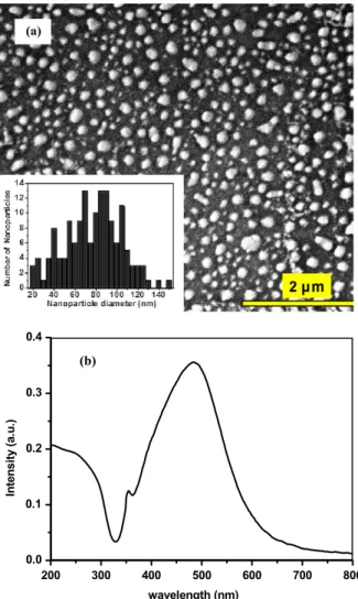
Figure 2(a) shows a typical SEM image (FEI Nova Nanosem 430) of the Ag-NCs formed on glass substrate after RTA treatment. Particle sizes 20–150 nm are observed with a distribution as shown in the inset. The absorption characteristics of the Ag-NC thin film formed with the above technique were obtained with a Varian Cary 5000 UV/vis/NIR spectrophotometer. The spectral absorption of the Ag-NC films, figure2(b), exhibits a broad absorption peak centered
Figure 1. (a) Cross-sectional diagram of the fabricated Si-NC PD. (b) SEM image, top view of the fabricated Si-NC PD.
around 490 nm. Ag-NCs absorb light into localized plasmon modes as explained earlier [44]. In the completed device, the Ag-NCs are obtained on Si substrate and are covered by a Al2O3 layer. The absorption peak is expected to shift to
larger wavelengths due to the higher refractive indices of the surrounding materials (compared to Ag-NCs on glass).
The electrical characterization of the fabricated devices was performed with a commercial Keithley 4200-SCS type semiconductor parameter analyzer. Current–voltage (I–V) characteristics were obtained under dark conditions as shown in figure 3. The measured dark current densities of the devices are low, 30 mA cm−2, owing to the dual Al2O3
insulating layers. The dark current characteristics for samples with Ag-NCs show a characteristic increase of current after 5 V bias. This is attributed to the higher number of states available for charge tunneling owing to the presence of Ag-NC induced states at the Si–Al2O3interface. Repeatable
and scalable electrical characteristics obtained from different devices verify repeatable Si-NC coating.
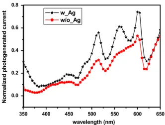
Spectral photogenerated current(Iphoto) is measured at
2 V applied electrical bias with a mechanically chopped, monochromated light normally incident on the device surface and a lock-in amplifier (SRS 830). Incident light power(Pin)
was measured with a calibrated Si photodetector. We used a bias voltage of 2 V in our photocurrent measurements. The measured photocurrent values are low compared to the literature [44]. This is attributed to the reduced collection efficiency of the photogenerated electron–hole pairs due to the presence of the dual Al2O3 layers that electrons and
holes should tunnel through. Figure 4 plots the normalized photogenerated current versus light wavelength from devices with and without a Ag-NC layer. The presence of Ag-NCs
Figure 2. (a) SEM image, Ag islands on quartz glass, inset: size distribution of Ag islands. (b) UV–vis absorption spectrum of Ag islands on quartz.
Figure 3. Dark current(I) versus bias voltage (V) spectrum, top curve Si-NC PD with Ag (solid line), bottom curve (dashed line) Si-NC PD without Ag.
introduced an additional peak around 550–570 nm. This is attributed to the plasmon resonance of Ag-NCs, which is in perfect agreement with the absorption profile of Ag-NCs as shown in figure 2(b). The absorption peak associated with
J. Opt. 14 (2012) 125001 S Alkis et al
Figure 4. Normalized photogenerated current versus wavelength (nm) spectrum: top curve Si-NC PD with Ag; bottom curve Si-NC PD without Ag.
Ag-NCs is red-shifted as predicted above, due to the larger dielectric constant of the surrounding Si substrate (compared to glass) and Al2O3 (compared to air), and a corresponding
shift of the localized plasmon resonance (from around 500 to 550 nm).
4. Conclusion
Visible range photodetectors are experimentally demonstrated using ultra-small Si-NCs obtained by laser ablation. Si-NCs films are achieved by the dip-coating technique. The absorption of the Si-NC layer is enhanced by Ag-NCs using localized plasmonic modes. Such Si-NCs could be used for ultra-low cost optoelectronic devices such as flexible and disposable sensors and low cost solar cells. Photodetectors that are fabricated based on such Si-NCs could offer new advantages over other types of photodetectors that are based on plasma-grown Si-NCs in large area optoelectronics applications by providing greater throughput and scalability.
Acknowledgments
This work was supported in part by European Union Framework Program 7 Marie Curie IRG Grant 239444, COST NanoTP, TUBITAK Grants 108E163, 109E044, 112M004 and 112E052, Ministry of Industry and Trade 636.STZ.2010-1. The State Planning Organization (DPT) of Turkey is acknowledged for the support from the UNAM Institute of Materials Science and Nanotechnology and the authors acknowledge support from TUBITAK BIDEB. The authors also thank Mr Adem Sarac¸ for the SEM imaging and Mr Semih Yas¸ar for his kind support with cleanroom experiments.
References
[1] Akcakir O, Therrien J, Belomoin G, Barry N, Muller J D, Gratton E and Nayfeh M 2000 Appl. Phys. Lett.76 1857
[2] Mitas L, Therrien J, Twesten R, Belomoin G and Nayfeh M 2000 Appl. Phys. Lett.78 1918
[3] Rogozhina E, Belomoin G, Smith A, Abuhassan L, Barry N, Akcakir O, Braun P V and Nayfeh M 2001 Appl. Phys. Lett.
78 3711
[4] Alkis S, Okyay A K and Ortac¸ B 2012 J. Phys. Chem. C
116 3432
[5] Hirano Y, Sato F, Aihara S, Saito N, Miyazaki S and Hirose M 2001 Appl. Phys. Lett.79 2255
[6] Nayfeh M H, Satish R, Nayfeh O M, Smith A and Therrien J 2005 IEEE Trans. Nanotechnol.4 660
[7] Shieh J M, Lai Y F, Ni W X, Kuo H C, Fang C Y,
Huang J Y and Pan C L 2007 Appl. Phys. Lett.90 051105
[8] Hu S F, Liao T W and Huang C Y 2007 Appl. Phys. Lett.
91 071125
[9] Kim S K, Kim B H, Cho C H and Park S J 2009 Appl. Phys. Lett.94 183106
[10] Takagahara T and Takeda K 1992 Phys. Rev. B46 15578
[11] Beard M C, Knutsen K P, Yu P, Luther J M, Song Q, Metzger W K, Ellingson R J and Nozik A J 2007 Nano Lett.7 2506
[12] Cho C H, Kim S K, Kim B H and Park S J 2009 Appl. Phys. Lett.95 243108
[13] Kim S K, Cho C H, Kim B H, Park S J and Lee J W 2009 Appl. Phys. Lett.95 143120
[14] Mafune F, Kohno J, Takeda Y, Kondow T and Sawabe H 2000 J. Phys. Chem.B104 8333
[15] Muramoto J, Inmaru T, Nakata Y, Okada T and Maeda M 2000 J. Phys. Chem. B104 9111
[16] Mafune F, Kohno J, Takeda Y, Kondow T and Sawabe H 2001 J. Phys. Chem.B105 5114
[17] Dolgaev S I, Simakin A V, Voronov V V, Shafeev G A and Bozon-Verduraz F 2002 Appl. Surf. Sci.186 546
[18] Yoshida T, Yamada Y and Takaaki O 1998 J. Appl. Phys.
83 5427
[19] Ehbrecht M, Kohn B, Huisken F, Laguna M A and Paillard V 1997 Phys. Rev. B56 6958
[20] Khokhlov E M, Kolmykov D V, Kononov N N, Kuzmin G P, Polyakov S N, Prokhorov A M, Sulimov N A and Tikhonevitch O V 1998 Laser Phys. 8 1070
[21] Kuzmin G P, Karasev M E, Khokhlov E M, Kononov N N, Korovin S B, Plotnichenko V G, Polyakov S N, Pustovoy V I and Tikhonevitch O V 2000 Laser Phys. 10 939
[22] Ledoux G, Guillois O, Porterat D, Reynaud C, Huisken F, Kohn B and Paillard V 2000 Phys. Rev. B62 15942
[23] Ledoux G, Gong J and Huisken F 2001 Appl. Phys. Lett.
79 4028
[24] Ledoux G, Gong J, Huisken F, Guillois O and Reynaud C 2002 Appl. Phys. Lett.80 4834
[25] Li X, He Y, Talukdar S S and Swihart M T 2003 Langmuir
19 8490
[26] Lacour F, Guillois O, Portier X, Perez H, Herlin N and Reynaud C 2007 Physica E38 11
[27] ˇSvrˇcek V, Sasaki T, Shimizu Y and Koshizaki N 2006 Appl. Phys. Lett.89 213113
[28] Yang S, Cai W, Zeng H and Li Z 2008 J. Appl. Phys.
104 023516
[29] Semaltianos N G et al 2008 Mater. Lett.62 2165
[30] Kuzmin G, Shafeev G A, Bukin V V, Garnov S V, Farcau C, Carles R, Warot-Fonrose B, Guieu V and Viau G 2010 J. Phys. Chem.C114 15266
[31] Amoruso S, Bruzzese R, Spinelli N, Velotta R, Vitiello M, Wang X, Ausanio G, Iannotti V and Lanotte L 2004 Appl. Phys. Lett.84 4502
[32] Semaltianos N G, Logothetidis S, Perrie W, Romani S, Potter R J, Edwardson S P, French P, Sharp M,
Dearden G and Watkins K G 2010 J. Nanopart. Res.12 573
[33] Rioux D, Laferriere M, Douplik A, Shah D, Lilge L, Kabashin A V and Meunier M M 2009 J. Biomed. Opt.
14 021010
[34] Intartaglia R, Bagga K, Brandi F, Das G, Genovese A, Di Fabrizio E and Diaspro A 2011 J. Phys. Chem. C
115 5102
[35] Yang S, Cai W, Zhang H, Xu X and Zeng H 2009 J. Phys. Chem.C113 19091
[36] Abderrafi K, Calzada R G, Gongalsky M B, Suarez I, Abarques R, Chirvony V S, Yu V, Timoshenko R I and Mart´ınez-Pastor J P 2011 J. Phys. Chem. C115 5147
[37] Sajti C L, Sattari R, Chichkov B N and Barcikowski S 2010 J. Phys. Chem.C114 2421
[38] Schaadt D M, Feng B and Yu E T 2005 Appl. Phys. Lett.
86 063106
[39] Kelly K L, Coronado E, Zhao L L and Schatz G C 2003 J. Phys. Chem.B107 668
[40] Pillai S, Catchpole K R, Trupke T and Green M A 2007 J. Appl. Phys.101 093105
[41] Stuart H R and Hall D G 1998 Appl. Phys. Lett.73 3815
[42] Lim S H, Mar W, Matheu P, Derkacs D and Yu E T 2007 J. Appl. Phys.101 104309
[43] Sundararajan S P, Grady N K, Mirin N and Halas N J 2008 Nano Lett.8 624
[44] Kim S K, Cho C H, Kim B H, Choi Y S and Park S J 2009 Appl. Phys. Lett.94 183108