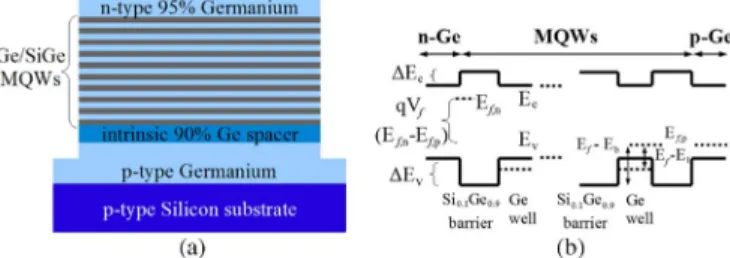
Ge/SiGe quantum well p-i-n structures for uncooled infrared bolometers
Tam metin
Şekil
Benzer Belgeler
In particular, feed- forward network provides lower bias in terms of the pricing performance relative to the Black-Scholes model; Black-Scholes mispricing worsens with
The main problems that are seen in Afghanistan are Civil War, Poverty, Inequality of Women, Environmental Problems:.. AFGHAN
As it mentioned previously, the EBD’s need a balance network at their BAL-port to follow the impedance seen from the ANT-port to provide the TX- to RX-port isolation. As a
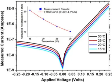
The doping dependent hole mobility in the various regions of device structure extracted from simulations presented in Figure 3 -a indicates that the hole mobility is
The transmitter block was planned to be fully integrated and the preceding circuits’s output impedance value may be easily matched to the input impedance of the power amplifier..
These can be listed as power gain, power output capability, power added efficiency (PAE), 1-dB compression point, intermodulation distortion (IMD), Adjacent Channel Power
The parasitic capacitance in the substrate is the dominant capacitance for medium to large value inductors, and the inductor resonant frequency is given using the circuit of Figure
In this dissertation, we have introduced a logistics and transportation simulation developed for use in the military DPP. We applied, for the
