www.advopticalmat.de
Nasim Seyedpour Esmaeilzad, Ahmet Kemal Demir, Jamileh Hajivandi, Hande Ciftpinar,
Rasit Turan, Hamza Kurt, and Alpan Bek*
DOI: 10.1002/adom.202000943
due to its abundance, nontoxicity, and establishment in the semiconductor industry for large-scale production. However, there are still many struggles regarding the material and processing costs associated with traditional wafer-based designs. For instance, a significant amount of incident light is reflected due to the high refractive index of Si, which causes a noticeable reduction in the con-version efficiency of solar cells.[1] There are
different methods utilized to reduce sur-face reflectance and improve conversion efficiency. Light trapping methods such as surface texturing, antireflection coatings (ARCs), and optical absorption enhance-ment via scattering from metallic or die-lectric nanoparticles are typical examples of such techniques.[2–10] Surface texture
can increase the light trapping by utiliza-tion of secondary incidence of reflected photons. However, most techniques for texturing Si require the use of a dry or wet etching process, which can be costly, time-taking, high in the energy budget, and harmful for the environment.
Single- or multilayered ARCs have simple, low-cost, and time-efficient fabrication processes. However, there are many limitations associated with the fabrication and performance of single- or multilayered ARCs such as poor adhesion, restricted working wavelength range, and limited working angle of the incident light. Furthermore, materials used for ARCs should be deposited carefully with precise refractive index and thickness control, which is quite challenging.
Alternative approaches in nanoscale light management in PV encompasses the employment of a vast range of dielectric nanostructures, such as nanowires,[11–16] nanoholes,[17] photonic
crystals,[18] nanocones,[19–21] and also metal nanostructures such
as nanoparticle arrays[22–24] and nanogrooves.[25] However, most
of these require multiple micro/nanofabrication steps which are not readily up scalable to cope with approximately km2
sur-face areas covered by PV plants. Moreover, structuring of the c-Si active region or introducing additional Si/metal interfaces in many of these approaches give rise to massive internal losses due to increased surface recombination.
Metal or dielectric nanospheres can be employed as an antireflection coating to solve the drawbacks mentioned above. Metal nanoparticles, which are integrated into the surface of Si solar cells (SCs), can avoid the detrimental effects on the elec-trical properties at the semiconductor surface.[6] They also offer
plasmonic effects and efficient radial charge-carrier collection. Furthermore, metal nanoparticles can scatter the incident light Dielectric colloidal nanospheres (NSs) are promising candidates for light
management in photonic devices such as solar cells (SCs). NS arrays can direct the broad incident solar radiation into a set of tighter foci, at which light intensity becomes considerably concentrated, enabling higher photo-voltaic conversion efficiency. Furthermore, the NS arrays acting as an effec-tive medium on the SC surface can reduce reflectance and facilitate improved forward scattering. Therefore, uniform arrays of NSs located on top of the SC can behave as antireflection coatings or as microlenses, which can be regarded as a surface distributed light concentrator within the framework of concentrated photovoltaics. Fabrication of NS-based light-trapping structures is low-cost and less complicated than common alternatives such as vacuum evaporated multilayer antireflection coatings. In this work, experimental dem-onstration and computational confirmation on the shape adjustment of such NS structures for improved light harvesting and efficiency enhancement in Si SCs are studied. The light conversion efficiency of Si solar cells is shown to improve by more than 27% with shape adjustment of NS arrays.
N. Seyedpour Esmaeilzad, H. Ciftpinar, Prof. R. Turan, Prof. A. Bek Center for Solar Energy Research and Applications
Middle East Technical University Ankara 06800, Turkey
E-mail: [email protected]
N. Seyedpour Esmaeilzad, H. Ciftpinar, Prof. R. Turan, Prof. A. Bek Micro and Nanotechnology Program of Graduate School of Natural and Applied Sciences
Middle East Technical University Ankara 06800, Turkey
A. K. Demir Physics Department I.D. Bilkent University Ankara 06800, Turkey Dr. J. Hajivandi, Prof. H. Kurt
Electrical and Electronics Engineering Department TOBB University of Economics and Technology Ankara 06560, Turkey
Prof. R. Turan, Prof. A. Bek Physics Department
Middle East Technical University Ankara 06800, Turkey
The ORCID identification number(s) for the author(s) of this article can be found under https://doi.org/10.1002/adom.202000943.
1. Introduction
Photovoltaic (PV) devices gain a considerable amount of atten-tion to fulfill our future needs as a renewable energy source. Silicon (Si) is one of the desired candidates for PV applications
into a large span of angles, which helps increase the path length of the light inside the absorbing layer.[26,27] However, depending
on their material type, size, and shape metal nanoparticles may have some downsides such as a significant amount of back-reflection and large ohmic (absorptive) losses, which sup-press the plasmon resonances. Besides, there are aging prob-lems associated with metal nanoparticles in which oxidation or sulfurization of their surface detriment their optical proper-ties in time. These drawbacks limit the applicability of metal nanoparticles as light management interfaces for SCs in com-parison to dielectric nanospheres (NSs).[28]
Light management using subwavelength dielectric NSs has become of interest in a wide range of PV platforms, such as amorphous silicon thin-film SCs,[29–32] GaAs thin film SCs,[33]
perovskite SCs,[34] ultrathin Si/graphene SCs,[35] and c-Si
thin-film SCs.[10] Polystyrene (PS) NSs are one of the
predomi-nantly used dielectric NSs which can be employed in diverse
applications such as antireflection coatings or microlens arrays in SC structures since they are scalable and low-cost.[36–40] PS
NS arrays can be coated onto large area solar cells with diverse nanosphere lithography technique.[41–44]
Naturally occurring hexagonal close-packed (hcp) arrays of NSs behave as an intermediate layer with the proper graded refractive index, which is between air and Si refractive indices. The graded refractive index facilitates the slow transition from air to Si and consequently enables light efficiently transmitting across the interface. Therefore, there is no need to use additional Figure 1. a) Layout of the Si SC with colloidal PS NSs. b)
Low-magnifica-tion top view of large-area hcp colloidal PS NSs on a Si SC. c) High-magni-fication top view of 750 nm colloidal PS NSs on Si SC. d,f,h) Side-view of 350 nm colloidal PS NSs on a Si SC after 10, 20, and 30 min of annealing, respectively. e,g,i) Side-view of 750 nm colloidal PS NSs on Si SC after 10, 20, and 30 min of annealing, respectively.
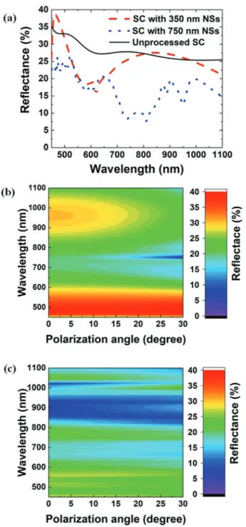
Figure 2. a) Simulated reflectance for unprocessed SC and with 350 and
750 nm colloidal PS NS coating. Simulated reflectance spectra versus polarization angle with b) 350 nm and c) 750 nm PS NSs.
materials with graded refractive indices. Besides, light is scat-tered after passing through NS arrays, which increases the effec-tive optical thickness of devices and light absorption through the conversion of light propagation angles from transverse to in-plane. External quantum efficiency (EQE), cell efficiency measurements, and simulation results can demonstrate the enhancement in the absorption over the solar spectrum.
An additional privilege of using PS NSs is that they can operate as optical microlens arrays, which concentrate the sunlight on to small regions of SC at which the radiation density can exceed typical AM 1.5 conditions where the Si SCs are more efficient. A topic referred to as concentrated PV (CPV). In this approach, an
apparent decrease in the required solar cell area offers an oppor-tunity to lower the material cost as high semiconductor material cost can be substituted with low-priced mirrors or lenses.
Novel strategies and materials can be inspected to achieve a reasonable cost range in CPV devices. Standard techniques for producing microlens arrays have some limitations. For instance, prevalent lens materials (i.e., glass) are usually heavy, costly, and hard to manufacture. Therefore, PS NS microlens arrays which require a low-cost and simple spin coating process can offer a reasonable replacement. In addition, by tuning the NS shape from that of an ideal sphere to nearly a hemispherical oblate shape can increase the amount of focused light inside the cell. Therefore, it is essential to understand the dependence of SC performance on the shape of the nanospheres.
In that respect, here we report the dependence of large area Si SC performance characteristics on shape modification of NSs using simple and fast annealing method, which is the main novelty of our work. Additionally, our electromagnetic simula-tions confirm the experimental results on various dimensions of nanospheres, representing that hcp NS arrays with 350 nm NS size improve the Si SC photoconversion efficiency by 27% and 750 nm NS size by 22%. Shape tunable light management feature of PS NSs have the potential for utilization in a multi-tude of photon devices.
2. Experiments and Simulations
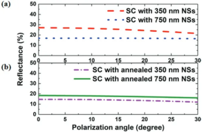
Si SCs are n+/p junction devices, which are fabricated from p-type monocrystalline Czochralski Si of 1–10 Ohm cm with Figure 3. a) Simulated weighted total reflectance (over 450–1100 nm
wavelength range) as a function of polarization angle for SCs with PS NSs. b) Same with annealed NSs.
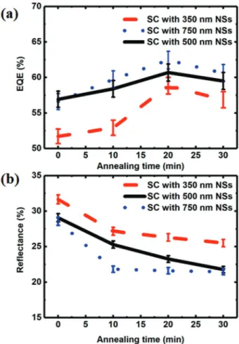
Figure 4. Experimentally determined EQE curves for shape-controlled NSs of a) 350 nm and b) 750 nm size. Experimentally determined reflectance
saw-damage-etched front side and textured backside. We pur-posefully keep the front side flat so that the photon manage-ment is solely performed by NSs and not by texture. The front surface side is plasma enhanced chemical vapor deposition (PECVD) coated with silicon nitride (SiNx) for protection before
KOH based texturing was applied to generate standard pyram-idal texture on the backside. In the following step, POCl3
diffu-sion in a quartz doping furnace was applied to generate the n+
doped emitter region.
The Si surfaces were passivated together by a dry oxidation process followed by PECVD deposition of a thin SiNx layer. The
oxide (≈5 nm) and SiNx (≈6 nm) layers are specially chosen to
be thin in order to enable good passivation but not to demon-strate any ARC effect themselves, so that the photonic effects of dielectric nanospheres are of the essence. To demonstrate the light concentration effect of NSs, the regular SiNx thickness of
80 nm used as ARC in standard crystalline SCs, is reduced to 6 nm. It should be noted that an 80 nm SiNx coating is not
reasonable to keep, since it displaces the NSs from the cell sig-nificantly, hampering the light concentration effect. Further-more, demonstration of antireflective effective index behavior of the small sized NSs would also be redundant while there is already an ARC. In the final step, an H-shaped silver grid is screen printed on the front surface as the front, while the rear side is fully covered by screen-printed aluminum as the back electrode. Activation of the screen-printed metal electrodes is provided by the cofiring step using an industrial conveyor belt furnace.
The surfaces of Si solar cells are made hydrophilic by the uti-lization of an oxygen plasma device. Then an aqueous suspen-sion of colloidal PS NSs was spin-coated on the SCs. An hcp PS monolayer was generated by self-organization after at least 24 h of drying. The PS NSs which are utilized in these sets of experiments are dispersed in water, and they are functionalized with hydroxyl group. The hydroxyl polar head group (OH) is anchored to the Si surface. After the adhesion of NSs to the Si, they can only be removed either completely by dissolving in acetone or partially by ultrasonic treatment if they are not ther-mally treated. However, once they are therther-mally treated even ultrasonication was found not to be sufficient to remove them from the surface. The diameters of PS NS employed here are 350, 500, and 750 nm.
The PS NS monolayer was uniform on the surface of the device. Modification of the NS shapes is performed by annealing. NS coated SCs are annealed on a hotplate at a tem-perature of 110 °C for 10, 20, and 30 min. By annealing NSs at 105–110 °C, we can attain changes in the shape of NSs within practical processing durations in a controllable manner that enable better light concentration effect, and improved effi-ciency. There is a narrow temperature margin of about 20 °C between which the results of thermal treatment are completely different (100–120 °C). After extensive shape optimization studies on NSs we have found that at ≥120 °C, NSs can be com-pletely molten, from which experimentally determined glass transition temperature (Tg) of PS NSs is found to be ≈110 °C
which agrees with literature.[45] The heat treatment induces the
spherical shapes of the NSs to modify into oblate spheroids, which leads to improvement in light focusing, in the sense that the foci of such formed micro-lens arrays shift more into the
device, better overlapping with the junction region and hence introducing improved efficiency. A perfect sphere, on the con-trary, generates a premature focus close to the top surface, and with severe chromatic aberration.
In our premises, we have conducted studies on the tempera-ture rise of the Si cells on a clear summer day previously. The temperature of cells was found to reach as high as ≈60 °C,[46]
which is well below the minimum temperature at which nano-sphere shapes start to change (>≈105 °C) at reasonable process durations. From our extensive optimization studies, we deter-mined that temperatures up to 95 °C are found to show no detectable influence on the nanosphere's shape/size regardless of the duration of temperature treatment. Thus, we can safely conclude that the nanospheres on the surface of solar cells are expected to hold their shape/size even on a clear summer day.
The electromagnetic simulations are performed using a finite elements method (FEM) Maxwell's equations solver, COMSOL,[47] to calculate the distribution of electric fields across
the boundaries of Si SCs, which can explain the light-harvesting effect of shape-controlled NSs and the absorption behavior of the devices. In these simulations, all the boundaries of the cal-culation box (4000 nm × 4000 nm x–y) were furbished with a perfectly matched layer (PML) boundary conditions (BCs).
Figure 5. a) Experimentally determined weighted total EQE (over
450–1100 nm wavelength range) as a function of annealing time for NSs of 350, 500, and 750 nm size and b) weighted total reflectance for NSs of 350, 500, and 750 nm size.
The reflectance of bare and NS coated SC surface, and the effect of shape modified NSs on reflectance is calculated using the finite-difference time-domain (FDTD) method. Polarization-dependent simulations are carried out using an FDTD Maxwell solver, Lumerical,[48] and were conducted between 0° and 30°
due to symmetry of hcp configuration. In all simulations, wave-length-dependent refractive indices and extinction coefficients of PS NSs and Si (dispersion effects) are taken into account.[49]
In the FDTD simulation, a calculation box with dimensions of (4000 nm × 4000 nm × 1000 nm x–y–z) has been implemented with PS NSs in hcp configuration on the surface. Along the x and y directions, BCs are chosen to be periodic and symmetric. Boundaries along the z-direction are furbished with PML BCs in order to avoid reflection of electromagnetic waves from the box boundaries.
3. Results and Discussions
The layout of Si SCs with colloidal PS NSs are sketched in Figure 1a, and a top-view SEM image of the SC surface is shown in Figure 1b. The low-magnification SEM image demonstrated in Figure 1c proves the uniform distribution of PS NS arrays. It can be seen that a single layer of PS NSs are self-organized
uniformly in hcp configuration on the surface of the SC, where the diameters of the PS NSs are confirmed to be ≈350, ≈500, and ≈750 nm with good monodispersity. 350 and 750 nm NSs are shown and 500 nm are omitted in Figure 1 for a clear com-parison. Figures 1d,f,h illustrate the annealing effect on the shape of 350 nm NSs after 10, 20, and 30 min at 110 °C, which manifests itself in reduction of the gap size between hcp NSs. Figure 1e,g,i shows tilted side-view SEM images of 750 nm NSs at increasing annealing times. Careful measurements of the spheroid dimensions are performed on close-up, side-view SEM images for detection of the differences between spheroid shapes meticulously, and simulations are carried out based on the shape data extracted from SEM images, which are provided in Figures S1 and S2 (Supporting Information).
3.1. Simulations and Experimental Results Supporting the Light Trapping (Antireflective) Effect
We have conducted electromagnetic simulations on reflectance from SCs with and without PS NSs at various incidence polari-zation angles only for 350 and 750 nm NSs since 500 nm NSs were experimentally found to produce an average photonic activity monotonously lying between the two. Moreover,
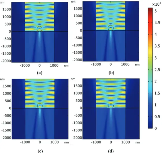
Figure 6. 2D cross-sectional E-field distribution at 600 nm wavelength calculated by the FEM (COMSOL) with 350 nm NS on Si SC: a) as deposited
utilization of smaller or larger size NS are found not to be favorable for optimal photonic effects (Figure S3, Supporting Information). Figure 2a shows that 750 nm NSs are effective as a broadband ARC coating whereas 350 nm NSs do perform best in 500–800 nm wavelength range. Figure 2b,c demonstrates that the ARC effect for both 350 and 750 nm NSs show little dependence on polarization, with 350 nm NSs demonstrating better ARC activity at polarization angles greater than 15° and 750 nm NSs virtually showing no significant dependence on
polarization. In order to have an understanding of the overall effect of the NSs, we have calculated weighted total reflec-tance as a function of the polarization angle, which is shown in Figure 3 for SCs with the two NS sizes before and after annealing. Small NSs with 350 nm diameter act as an effective index medium, exhibiting a thin-film interference pattern in the reflectance spectrum (Figure 2a). Their light concentration (microlens focusing) effect is negligible as compared to their effective index property. However, the light concentration effect takes the lead for NSs with a larger diameter (750 nm), and the effective index effect is reduced.
Figure 3 shows that shape control plays a crucial role in improving the graded-index behavior for all polarizations. The weighted reflectance of solar cells with NSs can be reduced significantly (>5%) by shape modification through annealing method for NSs of a significantly smaller size than the wave-length (350 nm). The change in the reflectance for larger par-ticles (750 nm) does show a similar reduction effect, albeit to a lesser extent (≈1%). Polarization-dependent simulations are performed between 0° to 30° due to symmetry of hcp configu-ration. The results strongly indicate a much preferred omnidi-rectional function of the shape tunable NSs.
The experimental results in Figure 4 show that there is a significant improvement in external quantum efficiencies of solar cells with shape-controlled nanospheres of both sizes. The reflectance is reduced only about an absolute 1% by 350 nm NSs in as deposited form, which increases up to a reduction of absolute ≈10% over the entire spectrum with shape control. The effect is similar in 750 nm spheres but to a greater extent. The reflectance reduces already by about absolute 5–10% in as depos-ited form, which increases to about 10–15% absolute reduction with shape control. It is obvious that significantly improved antireflective effect of NSs is possible through shape control. Detailed EQE and Reflection measurements for NSs of 500 nm are provided in Figure S4 (Supporting Information). Figure 5 displays the experimentally determined effect of annealing time on EQE and reflectance. At an annealing temperature of 110 °C, the ideal annealing time to achieve minimum reflectance and maximum EQE is found to be around 20 min.
Figure 7. a) 2D cross-sectional E-field distribution at 600 nm wavelength
calculated by the FEM method (COMSOL) for 10 min of annealing. Box dimensions 4000 nm × 4000 nm x–y. Same color map as in Figure 6. The junction zone is highlighted where the averaging is performed for parts (b) and (c). Calculated average intensity for different time-controlled shapes for b) 350 nm NSs and c) 750 nm NSs.
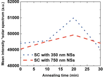
Figure 8. Simulated AM 1.5 solar spectrum weighted mean spectral
3.2. Simulations and Experimental Results Supporting the Light Concentration Effect
In order to demonstrate efficient control of the light concen-tration effect of NSs through shape control, E-field distribution profiles along the x–z plane are calculated at various wave-lengths using the FEM algorithm (COMSOL). Figure 6 shows time-averaged E-field amplitudes calculated at 600 nm
wavelength for the as deposited spherical 350 nm NS on the SC as well as for its 3 different shape modified versions. In order to conduct the simulations, the shapes of the NSs are determined from high magnification SEM images. Thereby, dimensions and oblate spheroid shapes attained through annealing pro-cesses are transferred to the simulations as precise as possibly representing the experimentally obtained shapes.
As it is not easy to discern the subtle-at-first-sight differences between the cases in the overall look given in Figure 6, we have decided to conduct our more detailed analysis close to the junc-tion region. In order to understand the effect of light concen-tration, cross-section averaged E-field intensities are calculated over a 200 nm thick region surrounding the junction plane at 400 nm below the surface in all cases. The average field intensi-ties are given as a function of wavelength in Figure 7 for both 350 and 750 nm NSs.
In order to have a sensible comparison between E-field profiles and experimental measurement of efficiencies, the mean E-field intensity of each configuration is multiplied with the solar simulator spectrum, utilized in experimental I–V measurements.
The resulting spectrally weighted average intensities are plotted against annealing time as shown in Figure 8. The result shows that the optimal light concentration effect is expected from NSs annealed for 20 min, which agrees very well with the experimentally determined conclusion of Figure 5.
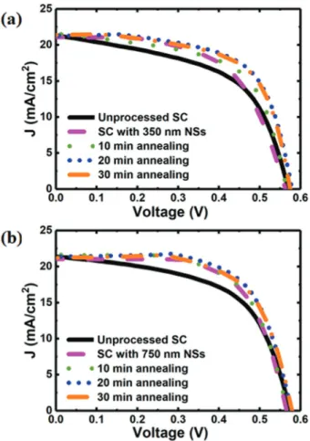
Figure 9. a) J–V measurements of SCs with 350 nm NSs at different
annealing times. b) Same with 750 nm NSs. Unprocessed reference cells are different for different NS sizes.
Figure 10. Experimentally determined a) photoconversion efficiencies;
b) FFs for SCs with 350 and 750 nm NSs versus annealing time.
Table 1. Efficiency and fill factor of shape-controlled NS SCs.
Sample FF % increase in FF η % increase in η Unprocessed SC 55.1 ± 1.1 – 7.5 ± 0.2 – 350 nm NSs 59.3 ± 1.2 7.7 8.1 ± 0.2 8.6 350 nm NSs 20 min annealing 65.4 ± 1.3 18.8 9.5 ± 0.2 27.6 Unprocessed SC 57.7 ± 1.2 – 7.9 ± 0.2 – 750 nm NSs 62.2 ± 1.2 7.9 8.6 ± 0.2 8.1 750 nm NSs 20 min annealing 66.2 ± 1.3 14.8 9.7 ± 0.2 22.0 Table 2. Jsc of shape-controlled NS SCs. Sample Jsc % increase Unprocessed SC 25.7 ± 0.5 – 350 nm NSs 26.6 ± 0.5 3.4 350 nm NSs 10 min annealing 27.4 ± 0.6 6.7 350 nm NSs 20 min annealing 30.4 ± 0.6 18.4 350 nm NSs 30 min annealing 29.0 ± 0.6 13.1 Unprocessed SC 23.5 ± 0.5 – 750 nm NSs 29.0 ± 0.6 23.4 750 nm NSs 10 min annealing 30.4 ± 0.6 29.4 750 nm NSs 20 min annealing 31.6 ± 0.6 34.3 750 nm NSs 30 min annealing 31.2 ± 0.6 32.6
For a more direct representation of the effect, experimen-tally obtained I–V curves are illustrated in Figure 9 for both 350 and 750 nm NSs. Here we see again that annealing time of 20 min optimized the light concentration effect. Namely, at the particular spheroid shape and size attained by 20 min of annealing time, the light focus is aligned to overlap best with the junction. We observe a similar improvement trend for both the efficiency and the fill factor (FF) in hcp NS covered SCs as shown in Figure 10, both of which agree with the simula-tion results of spectrally weighted average intensities given in Figure 8.
Table 1 summarizes the measured improvement of conver-sion efficiencies and fill factors for SCs with NSs and shape-controlled NSs. By employing a shape control mechanism, conversion efficiencies can be enhanced by >19% as compared to pristine NS light management and by >27% as compared to unprocessed SC.
Table 2 summarizes the measured improvement of Jsc for
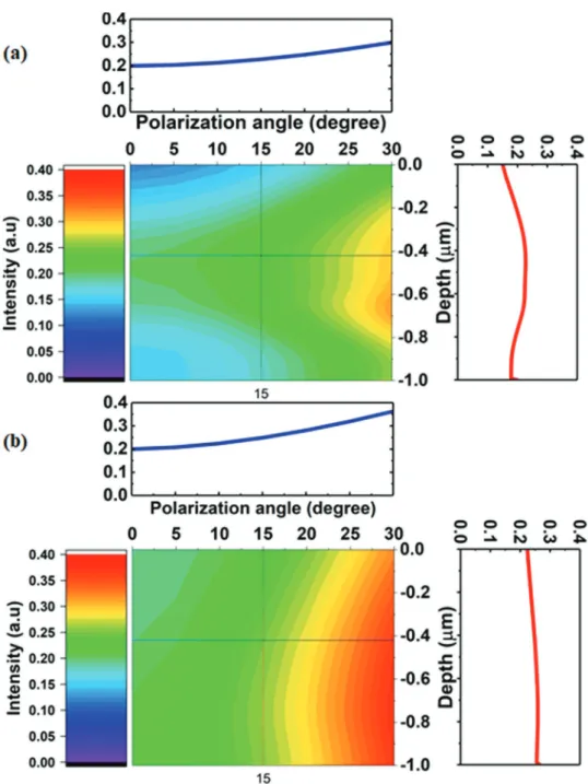
SCs with NSs and shape-controlled NSs. So, there is an increase in the photocurrent, which demonstrates enhanced absorption in the active layer due to the NSs’ light concentration effect. Therefore, it can be concluded that enhanced photovoltaic Figure 11. Simulated depth profile of E-field intensity versus polarization angle with a) as deposited 350 nm PS NSs and b) 20 min annealed PS NSs.
The horizontal line marks the approximate location of the junction, where the E-field amplitude profile is shown above the 2D plot. The vertical line marks 15° polarization where the depth profile to the right of the 2D plot is shown.
performance is not merely because of improved fill factor, but mainly because of improved absorption.
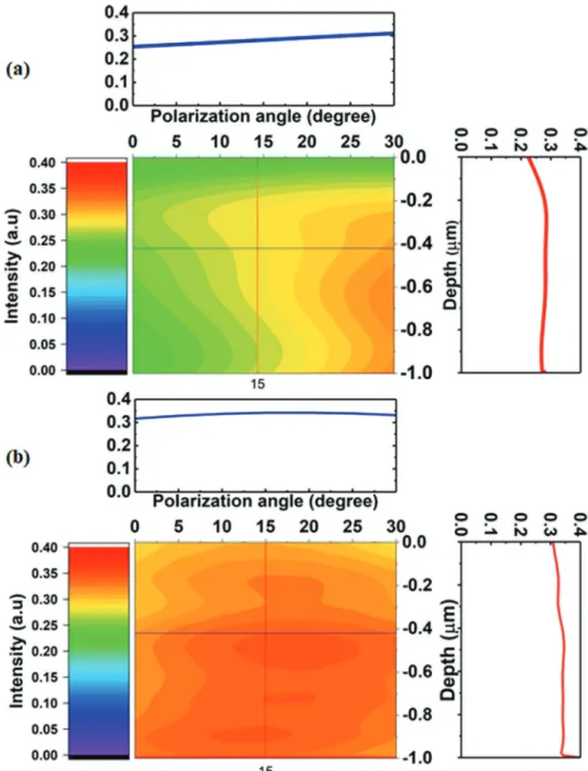
Figures 11a and 12a show polarization-dependent E-field amplitude depth profile at a wavelength of 600 nm within the Si SC calculated below the NS with 350 and 750 nm PS NSs, respectively. Figures 11b and 12b show the same calcu-lations conducted for the shape-controlled PS NSs. It is evi-dent that with shape control, the light concentration effect is enhanced for both NS sizes. Moreover, it can be observed that shape control does enable less polarization dependence
and more omnidirectional activity. The extent of the omni-directional polarization improvement in 750 nm NSs is far better than that of 350 nm with expressing virtually no dependence. The E-field intensity is found to be stronger for shape-controlled 750 nm NSs over a larger SC depth range, which indicates a better performance in light concentration than that of 350 nm NSs taking the long electron diffusion length in Si into account. Moreover, these results are found to be in good agreement with the experimental results of Figures 4 and 5.
Figure 12. Simulated depth profile of E-field intensity versus polarization angle with a) as deposited 750 nm PS NSs and b) 20 min annealed PS NSs.
The horizontal line marks the approximate location of the junction, where the E-field amplitude profile is shown above the 2D plot. The vertical line marks 15° polarization where the depth profile to the right of the 2D plot is shown.
4. Conclusion
In conclusion, a single layer of hcp PS NS arrays with 350 and 750 nm in diameter demonstrate antireflective and light concentration properties for single-crystalline Si SCs, which are significantly improved by low-cost, rapid, and uncompli-cated annealing-based NS shape control. There is a reduction of absolute 1% in reflectance for Si SCs with 350 nm NSs, which improves to an impressive absolute ≈10% over the entire spectrum with shape control. For Si SCs with 750 nm NSs, the reflectance is already reduced about an absolute 5–10%, which reaches to a striking absolute ≈10–15% with shape control. It is evident that the omnidirectional antire-flective properties of NSs can be intensified through shape control.
Furthermore, the shape-controlled PS NSs lead to better light concentration effect, which results in further improve-ments in conversion efficiency by a factor of 27% for SCs with shape-controlled 350 nm NSs and by a factor of 22% for SCs with shape-controlled 750 nm NSs. The novel idea of the shape-modification method for improved light management through NSs introduces an easily applicable and feasible way to achieve high-efficiency solar cells and has the potential for utilization in light management of many other kinds of photonic devices.
Supporting Information
Supporting Information is available from the Wiley Online Library or from the author.
Acknowledgements
This research was supported by The Scientific and Technological Research Council of Turkey (TÜBİTAK) under grant nr. 115F167.
Conflict of Interest
The authors declare no conflict of interest.
Keywords
concentrated photovoltaics, light management, nanospheres, shape adjustment, solar cells
Received: June 10, 2020 Revised: October 26, 2020 Published online: December 2, 2020
[1] G. J. Lin, H. P. Wang, D. H. Lien, P. H. Fu, H. C. Chang, C. H. Ho, C. A. Lin, K. Y. Lai, J. H. He, Nano Energy 2014, 6, 36.
[2] P. Matheu, S. H. Lim, D. Derkacs, C. McPheeters, E. T. Yu, Appl.
Phys. Lett. 2008, 93, 113108.
[3] H. R. Stuart, D. G. Hall, Appl. Phys. Lett. 1998, 73, 3815.
[4] S. Pillai, K. R. Catchpole, T. Trupke, M. A. Green, J. Appl. Phys. 2007,
101, 093105.
[5] D. Derkacs, S. H. Lim, P. Matheu, W. Mar, E. T. Yu, Appl. Phys. Lett.
2006, 89, 093103.
[6] D. M. Schaadt, B. Feng, E. T. Yu, Appl. Phys. Lett. 2005, 86, 063106.
[7] S. H. Lim, W. Mar, P. Matheu, D. Derkacs, E. T. Yu, J. Appl. Phys.
2007, 101, 104309.
[8] S. P. Sundararajan, N. K. Grady, N. Mirin, N. J. Halas, Nano Lett.
2008, 8, 624.
[9] Y. C. Chang, M. E. Pollard, D. N. R. Payne, A. Sprafke, S. Pillai, D. M. Bagnall, IEEE J. Photovoltaics 2019, 9, 1012.
[10] B. Wang, P. W. Leu, Nano Energy 2015, 13, 226.
[11] V. Sivakov, G. Andrä, A. Gawlik, A. Berger, J. Plentz, F. Falk, S. H. Christiansen, Nano Lett. 2009, 9, 1549.
[12] L. Tsakalakos, J. Balch, J. Fronheiser, B. A. Korevaar, O. Sulima, J. Rand, Appl. Phys. Lett. 2007, 91, 233117.
[13] D. R. Abujetas, R. Paniagua-Domínguez, J. A. Sánchez-Gil, ACS
Photonics 2015, 2, 921.
[14] S. W, X. L. Aixue Shang, X. Zhai, C. Zhang, Y. Zhan, Prog.
Photovol-taics Res. Appl. 2015, 23, 1734.
[15] B. Hua, B. Wang, M. Yu, P. W. Leu, Z. Fan, Nano Energy 2013, 2, 951. [16] G. Shalev, S. W. Schmitt, G. Brönstrup, S. Christiansen, Nano
Energy 2015, 12, 801.
[17] K. Q. Peng, X. Wang, L. Li, X. L. Wu, S. T. Lee, J. Am. Chem. Soc.
2010, 132, 6872.
[18] D. H. Choi, S. K. Nam, K. Jung, J. H. Moon, Nano Energy 2019, 56, 365.
[19] Z. Y. Wang, R. J. Zhang, S. Y. Wang, M. Lu, X. Chen, Y. X. Zheng, L. Y. Chen, Z. Ye, C. Z. Wang, K. M. Ho, Sci. Rep. 2015, 5, 7810. [20] B. Wang, P. W. Leu, Nanotechnology 2012, 23, 194003.
[21] C. M. Hsu, S. T. Connor, M. X. Tang, Y. Cui, Appl. Phys. Lett. 2008,
93, 133109.
[22] T. Gao, E. Stevens, J. Lee, P. W. Leu, Opt. Lett. 2014, 39, 4647. [23] L. B. Luo, C. Xie, X. H. Wang, Y. Q. Yu, C. Y. Wu, H. Hu, K. Y. Zhou,
X. W. Zhang, J. S. Jie, Nano Energy 2014, 9, 112.
[24] G. Liu, X. Liu, J. Chen, Y. Li, L. Shi, G. Fu, Z. Liu, Sol. Energy Mater.
Sol. Cells 2019, 190, 20.
[25] V. E. Ferry, L. A. Sweatlock, D. Pacifici, H. A. Atwater, Nano Lett.
2008, 8, 4391.
[26] T. Wang, S. Zou, J. Zhu, Z. Lu, H. Sun, X. Ye, L. Fang, R. Tang, X. Su,
AIP Adv. 2019, 9, 025218.
[27] Z. Sun, X. Zuo, Y. Yang, Opt. Lett. 2012, 37, 641.
[28] Y. A. Akimov, W. S. Koh, K. Ostrikov, Opt. Express 2009, 17, 10195. [29] C. L. Lee, W. S. Goh, S. Y. Chee, L. K. Yik, Photonics Nanostruct. -
Fundam. Appl. 2017, 23, 36.
[30] J. Grandidier, D. M. Callahan, J. N. Munday, H. A. Atwater, Adv.
Mater. 2011, 23, 1272.
[31] M. H. Elshorbagy, E. López-Fraguas, J. M. Sánchez-Pena, B. García-Cámara, R. Vergaz, Sol. Energy 2020, 202, 10.
[32] J. Grandidier, R. A. Weitekamp, M. G. Deceglie, D. M. Callahan, C. Battaglia, C. R. Bukowsky, C. Ballif, R. H. Grubbs, H. A. Atwater,
Phys. Status Solidi A 2013, 210, 255.
[33] J. Grandidier, D. M. Callahan, J. N. Munday, H. A. Atwater, IEEE J.
Photovoltaics 2012, 2, 123.
[34] Q. Luo, X. Deng, C. Zhang, M. Yu, X. Zhou, Z. Wang, X. Chen, S. Huang, Sol. Energy 2018, 169, 128.
[35] S. Das, M. J. Hossain, S. F. Leung, A. Lenox, Y. Jung, K. Davis, J. H. He, T. Roy, Nano Energy 2019, 58, 47.
[36] L. Li, T. Zhai, H. Zeng, X. Fang, Y. Bando, D. Golberg, J. Mater.
Chem. 2011, 21, 40.
[37] Y. R. Lin, K. Y. Lai, H. P. Wang, J. H. He, Nanoscale 2010, 2, 2765. [38] B. Wang, T. Gao, P. W. Leu, Nano Energy 2016, 19, 471.
[39] Y. Zhang, S. Chen, D. Hu, Y. Xu, S. Wang, F. Qin, Y. Cao, B. O. Guan, A. Miroshnichenko, M. Gu, X. Li, Nano Energy 2019, 62, 682.
[40] A. M. Al-Amri, P. H. Fu, K. Y. Lai, H. P. Wang, L. J. Li, J. H. He, Sci.
Rep. 2016, 6, 28671.
[41] G. D. Moon, T. Il Lee, B. Kim, G. Chae, J. Kim, S. Kim, J. M. Myoung, U. Jeong, ACS Nano 2011, 5, 8600.
[42] J. C. Hulteen, R. P. Van Duyne, J. Vac. Sci. Technol. A 1995, 13, 1553.
[43] C. L. H. And, R. P. Van Duyne, J. Phys. Chem. B 2001, 105, 5599. [44] B. Park, S. Y. Na, I. Bae, Sci. Rep. 2019, 9, 11453.
[45] J. Rieger, J. Therm. Anal. 1996, 46, 965.
[46] B. G. A. Talat Ozden, D. Tolgay, M. Samet Yakut, Turkish J. Eng.
2020, 4, 183.
[47] Detailed Explanation of the Finite Element Method (FEM), https:// www.comsol.com/multiphysics/finite-element-method (accessed: May 2020).
[48] Nanophotonic FDTD Simulation Software – Lumerical FDTD, https://www.lumerical.com/products/fdtd/ (accessed: April 2020). [49] X. Ma, J. Q. Lu, R. S. Brock, K. M. Jacobs, P. Yang, X. H. Hu, Phys.