PROCEEDINGS OF SPIE
SPIEDigitalLibrary.org/conference-proceedings-of-spieIntegrated asymmetric vertical
coupler pressure sensors
Isa Kiyat
Askin Kocabas
Imran Akcag
Atilla Aydinli
Integrated Asymmetric Vertical Coupler Pressure Sensors
Isa Kiyata, Askin Kocabasa, Imran Akcag and Atilla Aydinlia
aDepartmeflt of Physics, Bilkent University, 06800, Ankara, Turkey;
bDepartment of Electrical and Electronical Engineering, Bilkent University, 06800, Ankara,
Turkey
ABSTRACT
Design and analysis of a novel pressure sensor based on a silicon-on-insulator asymmetric integrated vertical coupler is presented. The coupler is composed of a single mode low index waveguide and a thin silicon slab. Wavelength selective optical modulation of asymmetric vertical coupler is examined in detail. Its potential for sensing applications is highlighted as an integrated optical pressure sensor which can be realized by standard
silicon micro-fabrication. Sensitivity of transmission of such couplers on refractive index change of silicon slab ensures that they are good candidates for applications requiring high sensitivities.
Keywords : Integrated Optics ,Wavelength-selective coupler, Pressure sensor, Stress-optic effect
1. INTRODUCTION
Pressure sensing by integrated optical means has always attracted much attention, since these sensors can typically operate at large temperature ranges, can be controlled remotely by optical fibres and are immune to electromagnetic radiation. They may also be designed to operate as passive optical components. Many complicated devices most of which are interferometric have been designed and fabricated so far .' 2 Mostof
these sensors are based on at least one integrated optical component (Mach Zehnder interferometer (MZI), ring resonator etc.) and some even use more than one.3 In a sensor using MZI, which is the most used interferometric design, a phase variation, which causes a shift the transmission spectrum is induced in the arm placed on a thin
diaphragm. These sensors generally achieve the necessary phase shift by an increase in the path length of the
arm through the elastooptic effect. Being relatively thick ('.-'50
t)
thesesensors have to be long (a few cm) toaccumulate the phase desired.4 The change in the interference pattern of the MZ can be used as a measure of the applied pressure. Similarly when a ring or an other resonator is utilized, applied pressure alters the transmission of the resonator and the pressure is sensed by measuring the shift in the resonance frequency.
Here, we utilize wavelength selective coupling between a low index single mode (SM) waveguide and a
mul-timode high index semiconductor slab waveguide. The backside of the chip is etched to get a thin diaphragm. The change in refractive index of the diaphragm under pressure alters the transmission spectrum which can be used to read out the applied pressure. The advantage of our design is that it can be used for both small
and large pressure measurements. Small pressures may be measured by locking input laser wavelength near but
not exactly at the coupling wavelength of the asymmetric coupler and monitoring the change in transmitted power while the pressure is applied. On the other hand, large pressures can be handled by using a tunable laser source and measuring the shift in the coupling wavelength. Finite element method (FEM) is used to predict the
behavior of the membrane under pressure while the optical response of the sensor is analyzed with the effective index method and the coupled mode theory. The results are confirmed by 2D beam propagation method (BPM) simulations.
A general detailed discussion on asymmetric vertical coupling with an emphasize on the couplers on silicon-on-insulator (SOT) substrates is given in section II. Section III describes design and basic operation principle of the pressure sensor including the coupler and the diaphragm specifications whit a brief discussion on elesto-optic effect. The paper ends with a discussion on sensor sensitivity in section IV and a conclusion section.
Further author information: (Send correspondence to A.A.) A.A.: E-mail: aydinli©fen.bilkent.edu.tr, Phone: +90 312 290 1579 Web:www.fen.bilkent.edu.tr/'iogroup
Figure 1. Two slab waveguides with different refractive index
2. ASYMMETRIC VERTICAL COUPLER
2.1. Theory
Whenever two optical waveguides are close enough, light may leak from one to the other through the coupling mechanism which is one ofthe mostly used physical effects in integrated optical devices, such as couplers, splitters, modulators and switches. The coupling between waveguides is generally analyzed by the coupled mode theory, predictions of which agrees extremely well with experimental results. In coupled mode theory, it is assumed that coupling changes the field amplitudes of modes, while their propagation constants remain unchanged.
Consider two slab waveguides in Figure 1. The guiding regions have different refractive indices of n1 and 2
while all cladding regions are with index of n. This is an example for non-degenerate or asymmetric vertical
coupler. We apply the coupled mode theory to this structure. We will not derive coupled mode equations and just make use of them. Derivations for these well known equations can be found in many introductory optoelectronics
books.5'6 The coupled equations that relate the field amplitudes of the waveguide modes are
dA1 .
—— = —3k21exp(3L3z)A2(z) (1)
and
dA
=
-jic12exp(jz@z)Ai(z) (2)here, the difference between propagation constants is given as
(3) and it is the measure of the phase mismatch. Also, ic21 and tt12 are coupling coefficients and are
1 k2 ph2+g+hi
=
-(n
—n)—
I
E1(y)E2(y)dy (4) 2 i3 Jh2+9 and 1i 22\ 0 I
k2 1h2/ \ / \_1
'12 =c)T
Je2y)61y)ay
P2.10for the mode fields ri and E2. The energy conservation of the system requires that the coupling coefficients
should be equal. Thus for the waveguide mode fields
(6)
R Co
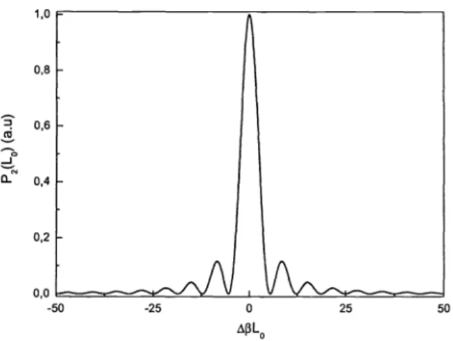
-J
Figure2. Power transferred as function of phase mismatch
Applying the initial conditions, ie. Ai(O) =1 and A2(O) =0,the equations can be solved to give two oscillating
solutions for Ai(z) and A2(z). Then, the optical powers are calculated by taking absolute square of the field amplitudes and found to be
2 z/3 2
Pi(z) =
cos (7z) + (--—)2sin (7z) (7)and
P2(z) =
()sin2(7z)
(8)where
2(fi)2+k2
(9)is the modified coupling coefficient when there is a phase mismatch.
The optical power exchanges between waveguides with the period -ir/y. The phase matching condition is
achieved when the waveguides are identical, that is L/3 =0. The distance required for full power exchange under phase matching condition is
7'-L0=—
(10)However, the power transferred has very interesting behavior at the distance L0 = when there is a phase mismatch between waveguide modes. It shows a diffraction like behavior and can be calculated using (8) and
(9) to be
P2(L0) =
()2sjnc2{'
[1 + (0)2]h/2}
(11)where sinc(x) =sin(rrx)/(irx) and the transmitted power is P1(L0) =1—P2(Lo). The transferred power can be understood better by drawing (11) as a function of L/3L0, Figure 2. Phase mismatch, z3 can also be written in
terms of effective index difference and free space wavelength as
eff
(12)(c)
C
Figure 3. Effective TE refractive index change with free space wavelength for highest order mode (m =6)of Si slab
with Si02 and air as lower cladding and SM BCB waveguide
2.2. SOT asymmetric vertical coupler
The coupled mode theory can be applied to a structure made of a low index waveguide on SOT substrate. It has been shown that such devices are highly wavelength selective . Inthat case, ni ,n2and n becomes indices of
silicon (-' 3.5), a low index material (1.5), and Si02 (' 1.46) respectively. If the low index waveguide is single
mode but silicon slab has several modes, which can be achieved by choosing h1 and h2 appropriately, it can be clearly seen that the fundamental modes of silicon slab and the low index waveguide are never phase matched. Therefore, no significant power coupling happens between fundamental modes. However, the dispersion of the
highest order mode of the silicon slab waveguide (see Figure 3. for the transverse electric (TE) mode) can be used to phase match them with low index waveguide mode. A simple mode analysis shows that fundamental mode has negligible dispersion compared to higher order modes. Thus effective index,nsm of single mode low index waveguide can be treated as constant. On the other hand,(Figure 3.) the highest order mode shows a
nearly linear behavior between two cut-off wavelengths and this dispersion can be written as
n(A) =
flAffl
+ mA (13)where flA0ffl 5 the effective index at smaller cut off wavelength and m is the associated slope in Fig. 3. Then,
the effective index difference becomes Lneff n(,\) —
sm
while phase mismatch is rewritten asz3
[fl;\ffl +
rnA;\_
flsm}27 (14)Therefore, transferred power (11) can be analyzed in the wavelength domain using (14).
What happens if a SM rib low index waveguide is placed instead of a slab waveguide to take advantage of butt coupling with a SM fiber? The solution is straight forward, mode analysis shows that mode dispersion of
such a waveguide is also nearly constant. Thus the modified transferred power (Eq. 11 with Eq. 14) can be used but sm becomes effective index of the rib waveguide.
3. DESIGN AND OPERATION OF THE SENSOR
3.1. Design
The sensor design allows it to be fabricated on a SOT wafer with a few micrometer top silicon thickness and a
buried oxide thickness large enough for optical confinement. The silicon slab has to be a multimode waveguide
in order to use in the asymmetric vertical coupler. Thus, we choose a SOT wafer with silicon and buried oxide
1510 1520 1530 1540 1550 1560 1570 1E Wavelength(nm)
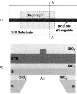
a)
b)
Figure4. Schematic top (a) and AA' cross sectional (b) views of the proposed SOT asymmetric integrated vertical coupler pressure sensor
thickness as 1.5 and 1 ,am for the sensor design, respectively. A 3 jm wide and 3im thick, benzocyclobutane
(BCB) SM rib waveguide with a rib height of 0.8 jm is placed on the SOl substrate after a 2 jtm Si02 deposition
on top of the silicon layer. The sensor structure can be seen in Figure 4.
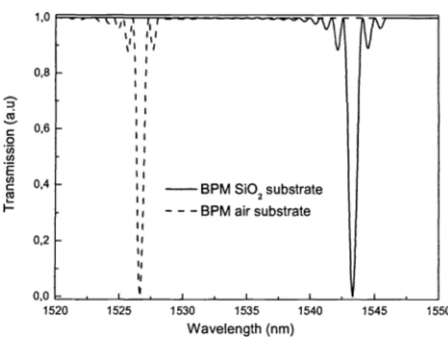
The refractive index of bulk BCB polymer is taken as 1.5339 at 1.55 ,am wavelength 8 TheBCB waveguide is simulated by BPM and found to be a single mode waveguide. Other low index materials, namely doped-Si02, SiXNV and SiON, can also be used as the low index SM waveguide. In Figure 5., effective indices of the BCB SM waveguide and the highest order mode of the Si slab waveguides with oxide and air substrates are given as a function of free space wavelength. It is clearly seen that, SM waveguide is phase matched with slab waveguides of different lower claddings at quite different and well separated wavelengths which we label as Aajr and A oxideS The sensor diaphragm can be defined by anisotropic KOH etch of silicon at the backside of the SOT wafer and
followed by a HF etch of the buried oxide. Thus, the lower cladding of the Si slab waveguide becomes air at the position of the diaphragm opening. The resulting structure (see Figure 4.) is a vertical coupler at these
selected wavelengths with different coupling lengths. The coupling lengths are functions of the deposited oxide
thickness and can be arranged to have coupling lengths of a few mm by BPM calculations (1725 jtm at the
resonance wavelength A=1526.5 nm). The coupling length for the vertical coupler with air lower cladding defines
the diaphragm length.
The transmission spectrums of the SM waveguide at calculated coupling length of about 1725 ,am are seen in
Figure 5. Tt should be noted that the bandwidth gets narrower as the coupling length and asymmetry between
waveguides increases while, narrower bandwidths results in higher sensitivities which can be achieved by highly asymmetric and well separated waveguides.
3.2. Stress-optic effect
As mentioned before, the pressure sensor makes use of the photo-elastic (or stress optic) effect which is the change in the refractive index of a material under applied stress. When external stress applied on the material,
Co 0 U, U) E U) C CO
Figure 5. Transmission spectrum of the SM waveguide integrated on the silicon diaphragm calculated using 2D BPM
the dielectric tensor (
r
) istransformed like a second rank tensor and can be written as()i =
(15)where Pi,j represents the strain optic coefficients and S3 represents the present strain. Here i =1,2, . .6represent
the strain components xx, yy, zz, yz, zx, xy, respectively. From Eq. 15, we get
n3 6
(16) Strain can be written in terms of the stress components to redefine (17)
ni =
6 (17)where C2, are the photo-elastic coefficients and ci are components of the stress. For isotropic medium have
two different values; longitudinal photo-elastic constant CL and transverse photo-elastic constant CT. Using
these constants, we can write refractive index changes for each direction as,
An =
CLTX+ CT(TY + crz) (18)Ln =
CLaY+ CT(o-X + az) (19)In =
CLcTZ+ CT(aY + o) (20)CL and CT can be defined as
CL =
(P11
—2up12) (21)
CT =
+
(1 —v)P12) (22)where Pu and P12 are the strain optical coefficient, Ti is the refractive index, while E and v are the Young's
Modulus and the Poisson ratio of the material, respectively. In Table 1, we summarize the stress optic coefficients
1530 1535 1540 Wavelength(nm)
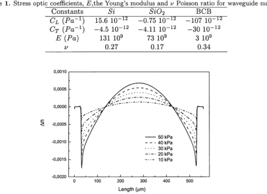
Table 1. Stress optic coefficients,
Constants
CL (Pa')
E,the Young's modulus and iiPoisson ratio for waveguide materials.
BCB
—107 10—12
Si
Si02
15.6 1O_12 —0.75 10—12
CT (Pa)
10—12 —4.11 10—12 —30 10—12E (Pa)
131 i09 73 i09 3 i09v 0.27 0.17 0.34 u,001U 0,0005 0,0000 -0,0005 -0,0010 -0,0015 -0,0020 ' ' ' , I . I . , 0 100 200 300 400 500 Length (tm)
Figure 6. The change in refractive index of the Si slab changes under applied pressure. The maximum change is on the edges and at the center of the diaphragm.
the Young's modulus and Poisson ratio for waveguide materials used in this design. Silicon has larger stress optic coefficient compared to Si02 and BCB. Knowing the stress components of the diaphragm layers which can be taken from FEM analysis for an applied pressure, the refractive index change in each direction can be calculated. Calculating Ln will be enough for TE polarization. The calculated index change can be used in
BPM simulations and/or the analytic transmission equation for asymmetric vertical coupler to study the response
of the coupler under pressure, that is, the change in transmission intensity and/or shift in coupling wavelength. The refractive index change for all layers constitute the diaphragm with applied pressure is calculated with 2-D FEM analysis and it is found that there is a linear relationship between index change and applied pressure
for all layers, as expected for elastic region of the materials. The analysis are first performed to find the optimum position the SM waveguide. The Figure 6., shows that the maximum refractive index change is on the edges and
at the center of the diaphragm. However, the waveguide should not be put too near the edges, because this will distort the slab waveguide operation of the silicon layer with the air as the lower cladding. The center of the
membrane is chosen as the place for the SM waveguide.
The choice of a polymer as SM waveguide material is due to the fact that its refractive index change under pressure is very small compared to silicon.9 It also behaves like a cushion between the 5i02 dielectrics and
avoids large stress. The Figure 7. shows a comparison of the index change of BCB and 5i02 layers with respect
to that of silicon slab. Thus, the effect of the BCB and the 5i02 layers are safely ignored in stress analysis.
4. DISCUSSION ON SENSOR SENSITIVITY
When the input laser wavelength is chosen near air while handling small pressures (smaller than 50 kPa) ,any
change in the refractive index of the system can be observed in transmitted intensity. In Figure 8(a)., the change
in transmission is given as a function of applied pressure. The net change in silicon index is calculated to be around 0.0005 for a pressure of 25 kPa. This change means a sensitivity of 0.14 rad.kPa' which is at least one order larger than the reported values.' Thus, the isothermal sensitivity of transmitted intensity is calculated
— 50 kPa — — - 4OkPa . . . . 3OkPa
—.—. 2OkPa
0004
1ii±iIII
0 50 100 150 200 250 300
Presure(kPa)
Figure7. The average refractive index changes of all the layers at the center of the diaphragm versus applied pressure. It is observed that the index change for silicon layer is at least 10 times larger than the changes for the other layers. Even
100 times in the case of the lower Si02 layer.
1,0 3,0
—U— Forlaser line put at 1526.6 nm
./
/
0,8/
/
I 2,5 S 7 .c 2,0::
/•/
) 1,5•//
,
::
. . , ,I
, , . , 0 10 20 30 40 50 0 50 100 150 200 250 300Pressure(kPa) Pressure (kPa)
a) b)
Figure8. (a)The transmission of the SM waveguide changes under applied pressure (low pressure regime) .Thelaser line is put at 1526.6 nm. (b)The central coupling wavelength of the asymmetric vertical coupler shifts under applied pressure
(highpressure regime). The laser is tuned over a few nanometers around the coupling wavelength with no applied pressure.
by zM/LP and is found to be 0.018 kPa1, where zM and LP are changes in transmitted intensity and pressure applied, respectively. It is seen that as the transmission dip gets narrower the intensity drops so the sensitivity
gets larger. This proposed design may be used for sensing even smaller refractive index changes therefore even smaller pressures (sub kilo pascals) with a slightly modified design.
For pressures larger than 50 kPa, the shift in coupling wavelength instead of the change in transmission is
monitored. This can be done by tuning the laser wavelength a few nanometers around the coupling wavelength
without applied pressure, Figure 8(b), for the shift in the coupling wavelength with high applied pressures. A similar sensitivity may also be calculated. We may call this "wavelength sensitivity" and define it as
where L.A is the shift in the coupling wavelength. It can be calculated to be about 0.01 nm/kPa for this pressure sensor. Such a measurement would be very straight forward with today's commercial tunable laser sources with wavelength stabilities as small 0.1 pm and intensity variations of around % 0.01.
5. CONCLUSION
A novel pressure sensor based on a SOT asymmetric integrated vertical coupler is designed and analyzed. The
proposed device is both easy to design and fabricate, compared to previous sensor designs. It uses well established silicon micromachining technology applied to SOT substrates. Newly developed SOT wafers with highly uniform
thicknesses are well suited for this device. The sensor comes out to be very sensitive due to dependence of transmission of the asymmetric coupler on refractive index of Si slab and can be used in both the low and high
pressure regimes.
ACKNOWLED GMENTS
This work was supported by Bilkent University Research Fund (Phys-03-02).
REFERENCES
1. G. N. De Brabander, J. T. Boyd and G. Beheim, "Integrated optical ring resonator with micromachanical
diaphgram for pressure sensing," IEEE Photon. Technol. Lett., 6, pp.671-673, 1994.
2. H. Porte, V. Gorel, S. Kiryenko, J-P. Goedgebuesr, W. Daniau and P. Blind, "Imbalanced Mach-Zehnder interferometer integrated in micromachined silicon substaret for pressure sensor," J. Lightwave Technol.,
17, pp. 229-233 1999.
3. C. Wagner, J. Frankenberger and P. P. Deimel, "Optical pressure sensor using two Mach-zehnder
interfer-ometers for the TE and TM polarization," J. Micromech. Microeng., 4, pp. 35-39, 1994.
4. C. Wagner, J. Frankenberger and P. P. Deimel, "Optical pressure sensor based on a Mach-zehnder
interfer-ometer integrated with a lateral a-Si:H p-i-n photodiode," IEEE Photon. Technol. Lett., 5pp. 1257-1259,
1993.
5. B. E. A. Saleh and M. C. Teich, Fundamentals of Photonics, John Wiley & Sons, NY, 1991. 6. Pollock C. R., Fundamentals of Optoelctronics, Richard D. Irwin Tnc.,Chicago, 1995.
7. B. Pezeshki, F. Agahi, J. A. Kash, J.J Welser and W-K. Wang, "Wavelength selective waveguide
photode-tectors in silicon-on-insulator" Appl. Phys. Lett. 68, pp. 741-743, 1996.
8. Dow chemical data sheet for BCB.
9. D. Hah, E. Yoon and S. Hong, "An optomechanical pressure sensor using multimode interference
coupler-swith polymer wavguides on a thin p+-Si mabrane," Sensors and Actuators, 79 pp. 204-210, 2000.
10. M. J. Weber Handbook of Laser Science and Technology, CRC, Boca, FL,1986. 11. ILX Lightwave Corp. Tunable laser Source TLS 8800 Series