An Optical Microcantilever with Integrated Grating Coupler
Selim Oleum', Ertugrul Karademir', Vahdettin Tast, Imran Akca, Askin Kocabas', Abdullah Atalar' and Atilla Aydinli2
1Department ofElectrical and Electronics Engineering, Bilkent University, 06800 Bllkent Ankara, TURKEY
1Physics Department, Bilkent University, 06800 Bilkent Ankara, TURKEY
Microcantilevers are used in a wide range of applications including atomic force microscopy systems and biosensing applications. External nanomechanical forces applied on the microcantilevers are measured by monitoring the deflection of the cantilever tip. The detection methods used for monitoring the tip deflection includes optical reflection or piezoresistive sensing. In this work, we demonstrate an easy to fabricate optical waveguide cantilever with a diffraction grating coupler at the tip, using a process compatible with standard micro fabrication techniques.
The optical cantilever with an integrated grating region at the tip is proposed to be used in atomic force microscope systems and other sensing applications. The period of the grating at the tip is chosen such that the incoming light can be coupled into the silicon microcantilever. The proposed incoming laser wavelength is 1.5
urn
and the grating period is approximately 530 nm. Silicon-on-Insulator (SOl) wafers have been chosen for thefabrication of the cantilevers. The thickness of the cantilevers is 3 urn; however, thicker active layers (5-10 microns) can be used for higher resonance frequencies. Several different cantilevers with widths of 40 um and different lengths and single mode and multimode ridge waveguide structures with varying widths were designed to couple light from the grating to the output port .
The fabrication of the structure starts with a master grating which is fabricated using the holographic lithography technique. The grating at the tip of the microcantilever is fabricated by replicating this master grating
onto a Polydimethylsiloxane (PDMS) mold using nanoimprint lithography. A UV curable polymer(00146) is
spun on the SOl wafer and the mold is used to imprint the grating onto the polymer. After UV exposure to cure the polymer, PDMS mold is peeled off leaving behind a grating on the polymer coated Si layer. Reactive ion etching (RIE) is employed in order to transfer the polymer grating to the silicon layer. The process duration and conditions are optimized for the best grating profile since they are critical for the coupling of light to the top Si
layer of the cantilever. After removing the photoresist and the excess OG146by a piranha etch, the cantilevers
are patterned and etched by RIE resulting in gratings at the tip of the cantilever as shown in Figure 1. The fabrication process is concluded by integration of the ridge waveguide at the support region of the cantilever and cleaving of the sample .
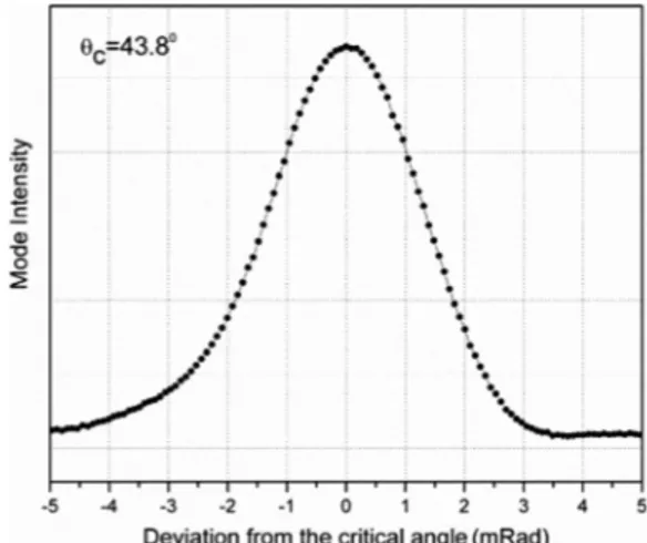
The measurements are taken using a laser diode with 1.5 urn wavelength. The angle of incidence is scanned while the optical power at the end of the ridge waveguide is monitored by a power meter. The intensity of the measured mode seen in Figure 2 has a full width of half maximum of approximately 3 milliradians. Detailed noise analysis shows that these cantilevers are promising for future applications.
In summary, we have fabricated an optical cantilever with an integrated grating coupler. We have used an
inexpensive and repeatable method for integrating the grating to the silicon cantilever with a micro fabrication compatible process . The sensitivity of the method can be further increased by integrating the detection circuitry onto the cantilever substrate. We believe that this is a promising method for sensing applications which provide a simple yet sensitive measurement technique using microcantilevers.
·5 -4 ·3 ·2 . , 0 1 2 3 4
Devia!ion from the critical angle (mRad) ~ 'iii c: $ c:
.,...
.
.
.
.
. .
~ ~ ~.
.
.
f ,.
.
J- .-\ l :e.
~ ~.
:..
.
~ : ~ j.
~ ~. e.:.
.
:.
~.
• ie.
o _ • • ...~. _,Figl.SEM imageof the grating at the tip of the cantilever
978-1-4244-4080-1 /09/$25.00 @2009IEEE
Fig. 2. Intensityof the coupled mode with respectto the deviationfrom the critical angle,