' • W y іХ->г;і г- - - -г^ ' ' · · ' - -'--.■г -г - і - - . г ѵ -г л
'.---i'ív Ö İ'İJ/IN İA İ 1->£L·i Δ(_.·i i O ı S iïlZ L -^ rlU _ y У Ѵ У . t J l ï y i i
- Я С & О М а С Ш І Ж В ü L T ' Ä i ^ G M ' " :
.^· >.·ν, ··- .·· ~.
i ) i k ■ ■
A DISSERTATION
SUBMITTED TO THE DEPARTMENT OF ELECTRICAL AND ELECTRONICS ENGINEERING
AND THE INSTITUTE OF ENGINEERING AND SCIENCES
OF BILKENT UNIVERSITY
IN PARTIAL FULFILLMENT OF THE REQUIREMENTS
FOR THE DEGREE OF DOCTOR OF PHILOSOPHY
By
Arif Sanli Ergun
April 27, 1999
тк
5 9 δ 2 • E H
for the degree of Doctor of Philosophз^
A h
Abdufiah Atalar, Ph. D. (Supervisor)
I certify that I have read this thesis and that in my opin ion it is fully adequate, in scope and in qualit)', as a thesis for the degree of Doctor of Philosophy.
yrettin Koymen, Ph. D.
I certify that I have read this thesis and that in my opin ion it is fully adequate, in scope and in quality, as a thesis for the degree of Doctor of Philosophy.
I certify that I have read this thesis and that in my opin ion it is fully adequate, in scope and in quality, as a thesis for the degree of Doctor of Philosophy.
Ekmel 0zMiy,4^h. D.
I certify that I have read this thesis and that in my opin ion it is fully adequate, in scope and in quality, as a thesis for the degree of Doctor of Philosophy.
Mustafa Karaman, Ph. D.
Approved for the Institute of Engineering and Sciences:
. S
i t
Prof. Dr. Mehmet
A NEW SIGNAL DETECTION METHOD FOR CAPACITIVE
MICROMACHINED ULTRASONIC TRANSDUCERS
Arif Sanlı Ergun
Ph. D. in Electrical and Electronics Engineering
Supervisor: Prof. Abdullah Atalar
April 27, 1999
Capacitive micromachined ultrasonic transducers (cMUT) have become an alternative to piezoelectric transducers in the past few years. They are constructed by integrat ing many small circular membranes in parallel. In this thesis, we demonstrate a new signal detection method for cMUT’s. We model the membranes as capacitors, and the interconnection lines between the membranes as inductors. The resulting circuit is an artificial transmission line with a certain electrical length. The vibrations of the mem branes modulate the electrical length of the transmission line, which is proportional to the frequency of the signal through it. By measuring the electrical length of the artificial transmission line using a high RF frequency (in the GHz range), the vibrations of the membranes can be detected in a very sensitive manner. Typically, the improvement over the conventional method is two orders of magnitude. For the devices we measured we observed a minimum detectable displacement in the order of 10"^ A / V ^ .
Keywords: capacitive micromachined ultrasonic transducers, ultrasonic signal detection,
ÖZET
KAPASİTİF MİKRO-İŞLENMİŞ ULTRASONİK ÇEVİRİLER İÇİN
YENİ BİR SİNYAL ALGILAMA METODU
Arif Sanlı Ergun
Elektrik ve Elektronik Mühendisliği Doktora
Tez Yöneticisi: Prof. Dr. Abdullah Atalar
27 Nisan 1999
Geçtiğimiz bir kaç sene içerisinde kapasitif ultrasonik mikro-işlenmiş çeviriciler (kUMÇ) piezoelektrik çeviricilere alternatif olmaya başladilar. kUMÇ’lar çok sayıda küçük daire sel zarların paralel şekilde bir araya getirilmesiyle oluşturulmaktadır. Bu tezde kUMÇ’lar için yeni bir sinyal algılama yöntemi gösterilmektedir. Bu yöntemde zarlar kondansatör, zarlar arasındaki bağlantılar ise indüktör olarak modellenmektedir. Ortaya çıkan devre yapay bir iletim hattı olup belli bir elektriksel uzunluğu vardır. Zarların titremesi du rumunda yapay iletim hattının elektriksel uzunluğu değişir, ve değişim miktarı hattan geçirilen sinyal frekansı ile doğru orantılıdır. Yüksek bir RF frekansı kullanılarak (GHz seviyelerinde) yapay iletim hattının elektriksel uzunluğu ölçüldüğünde zarlardaki titreşim oldukça hassas bir şekilde algılanabilmektedir. Tipik olarak, bu 5^eni yolla yapılan ölçümlerde geleneksel yollarla yapılan ölçümlerden yüz kat daha fazla hassasiyet elde edilebilmektedir. Denediğimiz çeviricihude ölçülebilen en düşük bükülme 10"’^ Â /\/Hz seviyelerinde gözlenmiştir.
Anahtar Kelimeler: kapasitif mikro-işlenrniş ultrasonik çeviriciler, ultrasonik sinyal algılama,
It took more than two and a half years for this thesis to come to existance with the contribution of many people. Above all, I would like to thank Prof. Abdullah Atalar who has always been positive with the work we did.
I would also like to thank Dr. Ekmel Ozbay for his strong support and guidance in our work at the Advanced Research Lab. Here, I have to mention about the research team in the Advanced Research Lab with gratitude. They have always been helpful.
Many thanks to Ayhan Bozkurt, Burak Temelkuran, and Dr. Erhan Polatkan Ata for their invaluable discussions, and immediate solutions to the problems we met. Without them, this work would not be that enjoying.
Finally, I want to thank to Alev, my friends and my family for their great support and patience during our work. Without them, this work would not be that meaningful.
Contents
1 IN T R O D U C T IO N 1 2 TH E N E W D E T E C T IO N M ETH O D 4 2.1 Mathematical fo rm u la tio n ... 6 2.2 Interferometric D etection... 8 2.3 Direct Detection 102.4 Sensitivity and the effect of the l o s s ... 13
3 D E V IC E FA BR IC A TIO N 17
3.1 Process Steps 18
3.1.1 Normal Lithography & M etalization... ... . 19 3.1.2 Image Reversal Lithography and M e ta liz a tio n ... 22 3.1.3 Sacrificial Layer Growth and Patterning 23 3.1.4 Hard-baked photoresist as a Sacrificial L a y e r... 25 3.1.5 Bridge M etalization... 26
3.2 Process Details 28
3.2.1 Mask Design... 28 3.2.2 Sample cleaning... 28
3.2.3 CPW Metalization 29
3.2.4 Sa.crificial L a y e r... 29
3.2.5 Bridge Adetalization... 30
3.2.6 Pad M e ta liz a tio n ... 30
3.3 The Designed Masks 30 3.3.1 Unit C e l l s ... 31
3.3.2 Mask level process s t e p s ... 31
4 E L E C TR O M A G N E TIC SIM ULATIONS A N D P R E D IC T IO N S 37 4.1 Frequenc)^, fo and Substrate D ependence... 39
4.2 Metalization Thickness, t Dependence... ... 44
4.3 Capacitor Width, wc D ependence... 46
4.4 Capacitor Length, Ic D ependence... 49
4.5 Bridge Height, xq D ependence... 52
4.6 Center Conductor Width, w D ependence... 55
4.7 Center Conductor to Ground Gap, g D e p en d e n ce ... 58
5 E X PE R IM E N T A L RESULTS 61 5.1 Measuring the Bridge Height and the Spring Constant of the Bridges Using Surface Texture A n a ly z e r... 62
5.1.1 Static Behavior of the B rid g es... 62
5.1.2 The M easu rem en ts... 64
5.2 Measuring the Lumped Element Values Using S-param eters... 69
5.2.1 S-parameters and extracted Za, a, 0o, L, Co, V2 and Ri values . . 71
I X
5.3 Low Frequency Experiments with Interferometric D etection...100 5.3.1 Measurement of the static response of the bridges with interfero
metric detection...102 5.4 Excitation Experiments with Direct D e te c tio n ... 110 5.4.1 D3marnic Behavior of the B r id g e s ... 110
5.4.2 The measurements 111
5.5 Detection E x p erim en ts... 120 5.6 Extracting the Mason’s equivalent circuit for the a ir-b rid g e s ...124
6 C O N C L U SIO N 126
A A rtificial Transm ission Lines 128
B Inductors 131
1.1 Cross-section of a typical membrane. 2 2.1 The lumped-element circuit model of a detector with 5 e le m e n ts... 5 2.2 The electrical model of the detector. 6 2.3 The Interferometric method to measure the phase-modulation... 9 2.4 The normalized plot of the envelope voltage as a function of the phase
difference between the two arms of the interferometer... 11 2.5 Alternative electrical model of the detector. 11 2.6 The direct method to measure the phase-modulation... 13 2.7 The normalized sensitivity as a function of the phase difference between
the two arms of the interferometer. 14 2.8 A single section lossy artificial transmission line: The lumped element
model of a membrane with its interconnections. 16 3.1 A section of an artificial transmission line with an air-bridge... 18 3.2 SEM photograph of an artificial transmission line section with an air-bridge. 18 3.3 Simplified diagram of an air-bridge process. 19 3.4 The la)'^out of the unit cell c32. 31 3.5 The first level: metalization... 33 3.6 The second level: pad metalization... 34
X I
3.7 The third level; bridge posts. 35
3.8 The fourth level: bridge metalization... 36
4.1 A closer look at an air-bridge. . . . ... 37
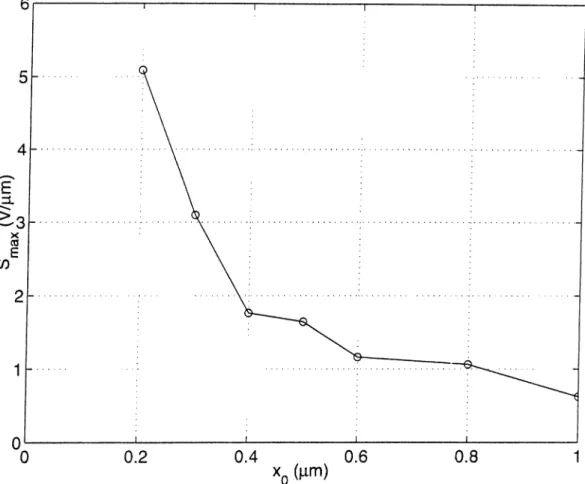
4.2 Sensitivity as a function of n and / 0. 41 4.3 Normalized maximum sensitivity as a function of cr... 43
4.4 Maximum sensitivity as a function of metalization thickness t ... 45
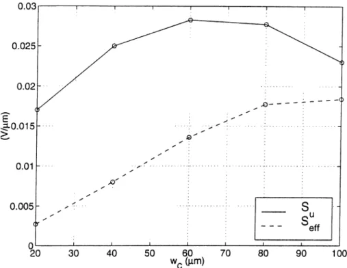
4.5 The calculated sensitivity as a function of capacitor width, w c ... 48
4.6 The calculated sensitivity as a function of capacitor width, w c ... 48
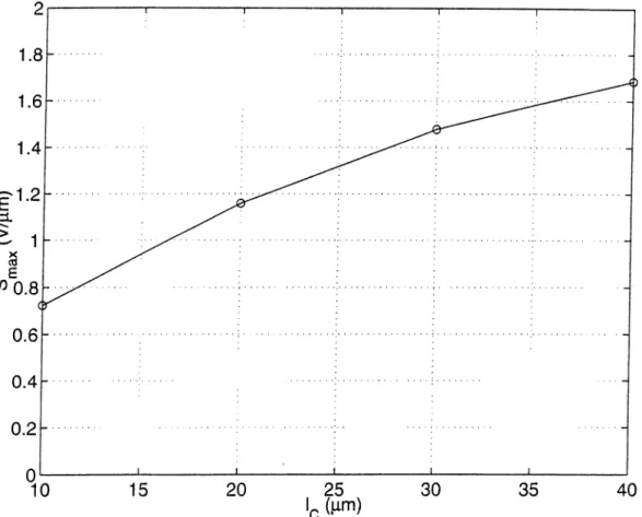
4.7 The calculated sensitivity as a function of capacitor length, Ic... 50
4.8 The calculated sensitivity as a function of capacitor length, Ic... 51
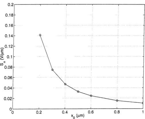
4.9 The calculated sensitivity as a function of bridge height, xq. 53 4.10 The calculated sensitivity as a function of bridge height, Xq. 54 4.11 The calculated sensitivity as a function of center conductor width, w. . . 56
4.12 The calculated sensitivity as a function of center conductor width, w. . . 57
4.13 The calculated sensitivity as a function of center conductor to ground gap, 9... · 59
4.14 The calculated sensitivity as a function of center conductor to ground gap, 9... 60
5.1 The measured bridge height of c l bridges as a function of the force applied: The spring constant is calculated from the slope, and the actual bridge height xo is extrapolated... 64
5.2 The measured bridge height of c2 bridges as a function of the force applied: The spring constant is calculated from the slope, and the actual bridge height .Xo is extrapolated... 66
5.3 The measured bridge height of c32 bridges as a function of the force applied: The spring constant is calculated from the slope, and the actual bridge height xq is extrapolated... 67 5.4 The measured bridge height of c33 bridges as a function of the force
applied; The spring constant is calculated from the slope, and the actual bridge height .tq is extrapolated... 68 5.5 S-parameters of a 22-section device with c l unit cells... 71 5.6 Complex characteristic impedance of the c l unit cell... 72 5.7 Attenuation and propagation constants of the c l unit cell where n=22. 73 5.8 Inductance and capacitance of the c l unit cell... 74 5.9 Loss resistances of the c l unit cell. 75 5.10 S-parameters of a 22-section device with c2 unit cells... 76 5.11 Complex characteristic impedance of the c2 unit cell... 77 5.12 Attenuation and propagation constants of the c2 unit cell where n=22. 78 5.13 Inductance and capacitance of the c2 unit cell... 79 5.14 Loss resistances of the c2 unit cell. 80 5.15 S-parameters of a 22-section device with c32 unit cells... 81 5.16 Complex characteristic impedance of the c32 unit cell. 82 5.17 Attenuation and propagation constants of the c32 unit cell where n=22. 83 5.18 Inductance and capacitance of the c32 unit cell... 84 5.19 Loss resistances of the c32 unit cell... 85 5.20 S-parameters of a 22-section device with c33 unit cells... 86 5.21 Complex characteristic impedance of the c33 unit cell. 87 5.22 Attenuation and propagation constants of th(! c33 unit cell where n=22. 88 5.23 Inductance and capacitance of the c33 unit cell... 89
xm
5.24 Loss resistances of the c33 unit cell... 90 5.25 Capacitance of the c l unit cell compared with the EM simulations. 91 5.26 Inductance of the c l unit cell compared with the EM simulations... 92 5.27 Series loss resistance of the c l unit cell compared with the EM simulations. 93 5.28 Capacitance of the c2 unit cell compared with the EM simulations. 94 5.29 Inductance of the c2 unit cell compared with the EM simulations... 95 5.30 Series loss resistance of the c2 unit cell compared with the EM simulations. 95 5.31 Capacitance of the c32 unit cell compared with the EM sim ulations.. . . 96 5.32 Inductance of the c32 unit cell compared with the EM simulations. . . . 97 5.33 Series loss resistance of the c32 unit cell compared with the EM simulations. 97 5.34 Capacitance of the c33 unit cell compared with the EA4 sim ulations.. . . 98 5.35 Inductance of the c33 unit cell compared with the EM simulations. 99 5.36 Series loss resistance of the c33 unit cell compared with the EM simulations. 99 5.37 The measurement setup in which the bridges are electrostatically deflected
with a DC bias... 103 5.38 The result of the detection experiment performed on electrostatically de
flected bridges. There are 74 bridges of type c l ...104 5.39 The result of the detection experiment performed on electrostatically de
flected bridges. There are 74 bridges of type c l with a bridge height distribution of as shown on the figure... 105 5.40 The result of the detection experiment performed on electrostatically de
flected bridges. There are 44 bridges of type c2...106 5.41 The result of the detection experiment performed on electrostatically de
flected bridges. There are 44 bridges of type c2 with a bridge height distribution as shown on the figure...107 5.42 The result of the detection experiment performed on electrostatically de
5.43 The result of the detection experiment performed on electrostaticall.y de flected bridges at 1 Hz. There are 44 bridges of type c2 with a bridge
height distribution as shown on the figure...109
5.44 The measurement setup in which the bridges are excited electrostatically using an AC signal... H I 5.45 Excitation experiment performed on c l unit cell. 113 5.46 Excitation experiment performed on c2 unit cell. 114 5.47 Excitation experiment performed on c32 unit cell... 115
5.48 Excitation experiment performed on c32 unit cell... 116
5.49 Excitation experiment performed on c33 unit cell... 117
5.50 Excitation experiment performed on c33 unit cell... 118
5.51 Excitation experiment performed on c34 unit cell... 118
5.52 Excitation experiment performed on c40 unit cell...119
5.53 Excitation experiment performed on c40 unit cell... 120
5.54 Excitation experiment performed on c38, c39 and c40 unit cells. 121 5.55 Detection experiment setup; RF signal source feeds the artificial line, and the signal source drives the piezoelectric transducer. The spectrum analyzer monitors the transmitted signal... 121
5.56 Si sample ; The output power measured as a function of RF signal frequenc}'. 122 5.57 GaAs sample ; The output power measured as a function RF signal fre quency... 123
A. l Single-section of a lossy artificial transmission line. 128 B. l A short section of a high impedance transmission line with a characteristic impedance of Zo and an effective dielectric constant of Cg//, and its lumped equivalent... 131
X V
C.l An electrostatic driving system with a fixed and a movable plate. C.2 Mason’s equivalent circuit for an electrostatic driving system. . . .
134 135
3.1 Geometrical parameters of the unit cells used... 32 4.1 The substrate parameters used for Si and GaAs where h is the substrate
thickness. 38
4.2 Geometrical parameters of an artificial transmission line section used in frequency, substrate conductivity and metalization thickness sweep simu lations... 40 4.3 Extracted lumped element values for GaAs substrate parameters. 40 4.4 Calculated values using the lumped element model with Fijf’= lV ... 40 4.5 Extracted lumped element values for Si substrate parameters. 41 4.6 Optimum n, and maximum sensitivity calculated from table 4.5... 42 4.7 Extracted lumped element values at 10 GHz using GaAs substrate pa
rameters and geometrical parameters th at are given in Table 4.2 with t as param eter... 44 4.8 Sensitivity values calculated using Table 4.7... 45 4.9 Geometrical parameters of an artificial transmission line section used in
capacitor width .sweep simulations. 46 4.10 Extracted lumped element values at 10 GHz using GaAs substrate pa
rameters and geometrical parameters given in Table 4.9. 47 4.11 Sensitivity values calculated u.sing Table 4.10. 47
X V I 1
4.12 Geometrical parameters of an artificial transmission line section used in capacitor length sweep simulations... 49 4.13 Extracted lumped element values at 10 GHz using GaAs substrate pa
rameters and geometrical parameters given in Table 4.12... 50 4.14 Sensitivity values calculated using Table 4.13. 50 4.15 Geometrical parameters of an artificial transmission line section used in
bridge height sweep simulations... 52 4.16 Extracted lumped element values at 10 GHz using GaAs substrate pa
rameters and geometrical parameters given in Table 4.15... 52 4.17 Sensitivity values calculated using Table 4.16. 53 4.18 Geometrical parameters of an artificial transmission line section used in
center conductor width sweep simulations. 55 4.19 Extracted lumped element values at 10 GHz using GaAs substrate pa
rameters and geometrical parameters given in Table 4.18... 55 4.20 The sensitivity values calculated using Table 4.19... 56 4.21 Geometrical parameters of an artificial transmission line section used in
center conductor to ground gap sweep simulations... 58 4.22 Extracted lumped element values at 10 GHz using GaAs substrate pa
rameters and geometrical parameters given in Table 4.21... 58 4.23 The sensitivity values calculated using Table 4.22... 59 5.1 Young’s Modulus and Poisson’s ratio of some metals as calculated from
the compliance constants [1]. 63
5.2 Calculated spring constant of the A1 bridges with = 80¡xm and tt, =
1.13/im. 64
5.3 Calculated and measured spring constant of the A1 bridges with k = 80/im and U = 1.13//rn... 65 5.4 Measured collap.se voltages of c l bridges and corresponding bridge heights. 101
5.5 Measured collapse voltages of c2 bridges and corresponding bridge heights. 101 5.6 Measured collapse \Oltages of c32 and c33 bridges and corresponding
bridge heights... 102 5.7 Measured values of AV,„u for Hias = lOV, S, and calculated value of S
according to EM simulations for unit cell c l ... 104 5.8 Measured AVout for Hio.? = lOV for unit cell c2... 105 5.9 Mason’s equivalent circuit values extracted for the air-bridges 125
Chapter 1
INTRODUCTION
Non-contact ultrasonic measurements and non-destructive evaluation are becoming more attractive with the development of high frequency, high efficiency, and sensitive trans ducers and transducer arrays. Armed with the basic advantage of being non-contact in nature they find many air-coupled and immersion applications in various areas. Among these, proximity sensing, surface fiaw detection, underwater imaging and biological scanning are the most popular ones. Conventional piezoelectric transducers that are used in ultrasonic measurements have quite large acoustic impedances (in the order of 10^ kg/m^s). In airborne applications the use of piezoelectric transducers is problem atic because of the low acoustic impedance of air (400 kg/m^s). The large impedance mismatch at the transducer-air interface introduces an enormous transmission loss, and decreases the coupling efficiency both in generation and detection of ultrasound. To overcome this mismatch, special matching layers can be used [2]. Although the use of matching layers solves the problem to some extent, this technique introduces other problems. Together with air backing, the increase in the coupling efficiency comes at the expense of a narrower bandwidth, and a limited high frequency performance [3,4]. Furthermore, the complexity introduced in the production process decreases the relia bility, increases the cost, and makes the fabrication of transducer arrays very difficult. Although the matching problem is much less serious in immersion applications, the inher ent problem of processing difficulty, low integrabilit}', and high temperature sensitivity of piezoelectric transducers persists.
sonic measurements both in air-coupled and immersion applications. Using the standard silicon processes developed in the past 30 years, along with micromachining technolog,y, scientists developed reliable, small, and cheap transducers and transducer arrays with comparable performance to piezoelectric transducers [5,6,8, 9]. These capacitive trans ducers consist of many circular membranes in parallel, and are used for both generation and detection of ultrasound. The cross-sectional view of a typical membrane is shown in Figure 1.1. The membrane is a thin layer of dielectric (usually SiNj) coated with a metal (usually Au) electrode. A post layer supports the membrane over the substrate. The substrate is conducting, and functions as a ground plane. The generation of ultra sound depends on the electrostatic attraction force between the top electrode and the substrate. When an alternating voltage with a large DC offset is applied to the elec trode, the membrane vibrates, coupling acoustic power into the medium. The amount of coupling reaches its maximum at the mechanical resonance frequency of the membrane. The mechanical resonance frequency and bandwidth are determined by the geometrical and structural properties of the membrane.
Figure 1.1; Cross-section of a typical membrane.
For ultrasonic applications in the MHz range, the size of a membrane is in the tens of microns order. The acoustic power coupled to the medium from a single membrane is very small and useless for all practical purposes. For this reason, many of these membranes are connected in parallel to generate reasonable ultrasound power. Surface micromachining technology is based on standard silicon processing techniques which is now capable of integrating millions of transistors. Therefore, thousands of these membranes can easily be integrated in a small area to obtain efficient and well-matched ultrasonic transducers.
The membrane that generates ultrasound is used for the detection of ultrasound as well. The electrode and the substrate make up a simple parallel plate capacitor. The detection of ultrasound depends on the vibration of the membrane due to an incident ul trasonic signal. The displacement of the membrane results in a capacitance change which
is measured by monitoring the current under a constant bias voltage. The magnitude of the current resulting from n parallel membranes can be expressed as,
/ = 27r/il4nC o—
Xo (1.1)
. where /1 is the ultrasound frequenc}c V^c is the bias voltage, Co is the capacitance of a single membrane, 2:0 is the separation between the electrode and. the substrate, and
A x is the magnitude of the displacement. The resulting current is then amplified with
a transimpedance amplifier. As it is clear in equation 1.1, the output is proportional to the total capacitance, the bias voltage, and the inverse of the gap length between the membrane and the substrate.
To increase the sensitivity of a cMUT as an ultrasonic detector we have three param eters to optimize. The first parameter is the bias voltage which is limited by the collapse voltage of the membranes. Since the membranes are useless after collapse, we have to keep the bias voltage as large as possible, but below the collapse voltage. The second parameter is the gap length between the membrane and the substrate. This parameter seems to be the most effective one, since a decrease in xq also increases the capacitance
Cq. However, the collapse voltage is proportional to x^q^'^\ and we have to decrease the
bias voltage as well if we decrease Xq. On the overall, the sensitivity is proportional
to the square root of 1/xo- Furthermore, the smallest Xq we can achieve is limited by
the technology. The final parameter that effects the sensitivity is the total capacitance. Both by increasing n and the area of each individual membrane it is possible to increase the sensitivity at the expense of an increase in the area.
The sensitivity also depends on the ultrasound frequency / 1. For high ultrasound frequencies we get better sensitivity. However, /1 is not a parameter that we can tune to increase the sensitivity. We have to design our transducer to operate at a certain frequency / 1. Therefore, for applications with low frequencies the detection sensitivity of the transducer degrades considerably.
In this thesis, we demonstrate an alternative method to detect the displacement of a membrane in a moi(! sensitive manner [10], [11]. Similar to the conventional method, our method is also based on the membrane capacitance variation upon receiving an ultrasound signal. However, as a major difference, we make use of a very high frequency RF signal (in the GHz range) instead of the DC bias voltage. It is this difference that improves the sensitivity by a few orders, and eliminates the sensitivity degradation at low ultrasound frequencies.
THE NEW DETECTION
METHOD
We ma}' view the DC bias voltage that is used in the conventional method as the probing signal of the detector. The quantit}' that is measured is the current out of the detector. The new method involves the use of a high frequenc}^ RF signal instead of the DC bias voltage as the probing signal. The measured quantity is the change in the phase of the RF signal.
The electrical model of a single membrane is a simple parallel-plate capacitor. The membranes are connected through interconnection lines. However small, these intercon nection lines can be modeled as lumped inductors. If the membranes are integrated in a series manner as shown in Figure 2.1, then the resulting lumped-element circuit model is an LC network which is called an artificial transmission line. Note that, the acoustical port of the detector is omitted for the time being because the frequency of interest at the moment ( GHz) is much higher than the mechanical resonance frequency of the detector ( MHz).
An artificial transmi.ssion line is made up of lumped inductors and capacitors. It can be viewed as an ordinary transmission line with a Bragg frequency as defined in Appendix A. For frequencies that are much lower than the Bragg frequency it is just like an ordinary transmission line. It has a characteristic impedance Za, and a propagation constant /5 determined by the L and C values as derived in Appendix A, and shown in
Figure 2.1: The lumped-element circuit model of a detector with 5 elements equation 2.1 where /o is the frequency.
( 2 . 1 )
0 = 27t/oVXC
The propagation constant ¡5 has units of radians per section. Thus, the electrical length ($o) of the artificial transmission line is
$ 0 = n X /?,
where n is the number of sections. At low frequencies, namely in the ultrasound fre quency range of concern, the electrical length of this artificial transmission line is very small. Practically, all the membranes are in parallel, and the detector is like a single lumped capacitor as usual. At RF frequencies that are much higher than the ultrasound frequency, the electrical length of the artificial transmission line becomes very significant, and the detector is like a distributed element.
At the quiescent position, the membranes have a definite capacitance, and the elec trical length of the line is fixed at <l>o· If a high frequency RF signal is applied from one of the ports, then the transmitted signal measured from the other port is a replica of the input with a phase shift that is equal to $o· When the membranes displace from their
ultrasound signal then the phase of the transmitted signal is modulated. The modula tion frequency is the ultrasound frequenc}^, and the modulation index is determined by the RF signal and the artificial transmission line properties. In the new method, the ultrasound signal is detected by phase-demodulating the transmitted signal.
2.1
M athem atical form ulation
Here, we include the acoustical port of the detector as shown in Figure 2.2 to make a proper mathematical formulation for detection. The electrical side consists of two transmission lines. One of them has a fixed electrical length which corresponds to the quiescent electrical length of the detector $o· The other one is a controlled phase-shifter whose length is controlled by the mechanical port. It accounts for the changes in the electrical length of the detector due to a displacement in the membrane. The mechanical port of the detector is modeled as usual which is the Mason’s equivalent [12].
Vi o ,0
{
AO=f(V)
+ y -%o oFigure 2.2: The electrical model of the detector. The membrane is a parallel-plate capacitor whose capacitance is
Cpp —
X
where A is the effective capacitor area, and x is the parallel-plate separation. In addition, there is always fringing capacitances which adds to the parallel-plate capacitance, and
do not change with x. The interconnection lines between the membranes are modeled as inductors (Appendix B) which is mostly true for high impedance and short lines. However, there is always a small parasitic capacitance associated with each inductor. This capacitance also adds to the parallel-plate capacitance. Defining the sum of the fringing and parasitic capacitances (or the capacitances which do not change with x) as C/, the total capacitance C at the membrane node is written as
C = ^ + Cf.
X (2,2)
Assuming a n-section artificial transmission line with identical membranes, the electrical length $ can be written using equation 2.1.
^ = n- 2 n M l L + Cf
X (2.3)
At the quiescent position of the membrane (x = xq) the total capacitance is denoted as Co = C{xo), the propagation constant and the electrical length are denoted as Po =
P{xo) and $0 = = iT-Po· The vibration of a membrane means that the parallel-plate
separation x vibrates around the quiescent position xq. As a result, the capacitance of the membrane, and the electrical length of the artificial transmission line vibrate around their quiescent values. We can expand $ around x — xq:
i^(x(t)) = $0 + (a:(t) - Xo)·
The phase-modulation term A ^( x ( t ) ) = $(x(t)) — $o can be written as, A/Tv/" Í4.W r?,27r/o\/LCo Cppo, , . . A$(.x(t)) = ---T--- j ^ { x { t ) - x o )
ZXo Uo
Tipo Cppo
{x{t) - Xo)·
2xo Co For a high frequency RF input signal of
K = V jip 008(271 J o t ) ,
the output of the detector (assuming Z„, ~ 50D) is
Vo = V,iroos[2Trfot - <i>o - A^)(x(i))].
Consequently, the outjmt of the detector is a phase-modulated signal.
(2.4)
the mechanical port to the current at the electrical port (Appendix C). Therefore, the transformer ratio denoted by ^p has the units of Coulomb/meter. Since we are using a different detection method, we modify Mason’s formulation, and define the transformer ratio as
-Vpp, (2.6)
_ ^o(^67ppq),
^ ---VRF·,
2xo
where Vrf is the R,F signal amplitude. We can write A$(a:(i)) as a controlled quantity as
where
A $(x(t)) = - F(x(t))
F
RF(2.7)
The displacement of the membranes (rr(i) — Xq) can be detected by measuring the
phase of the transmitted signal.
2.2
Interferom etric D etectio n
One way to obtain A<I>(x(t)) is to use an interferometer which is the basic method for phase measurements. In an interferometer, the input signal is divided into two arms, and then summed again as shown in Figure 2.3. The amplitude of an interferometer’s output is determined by the phase length difference between the two arms. The phase-length of the artificial transmission line is modulated by the vibrations of the membranes. The other arm has a fixed phase length, so the output of the interferometer is amplitude modulated. The vibrations of the membranes are obtained by envelope detection as shown in Figure 2.3.
The input to the interferometer is a cosine, = Vrpcos{27t f t) , whereas the output
is the sum of two cosine terms with different phases. To simplify the algebra, we express
1 on
w,in
Figure 2.3; The Interferometric method to measure the phase-modulation.
V,—
^1
-f· eJ[^i“*o-A4>(a:(i))]j gj27r/ot complex envelope(2.8)
which is an amplitude-modulated signal. The envelope of Ku is the magnitude of the complex envelope. Thus, the output of the envelope detector is,
VRF 2 ^RF 1 ^ gj[4>i-#0-A4>(rc(i))] = Vr f cos Î^V^2 [l + co s(< ï> i-$o-A $(a;(i)))] _ $0 A $ (.r(t))\ (2.9) B}' expanding the cosine term in equation 2.9 and using the approximations cos[A$(a:(i))] 1 and sin[A$(a;(t))] « A$(.x(t)), we obtain the output as
Vont = Vr f cos
-F Vrp sin
$1 - <î>c
$1 - $ o \ A $(x(i))
(2.10)
The quiescent phase difference between the two arms ($i - $ 0) is biased such that sin[($i — i>o)/2] is close to 1, but cos[(<I>i — i>o)/2] is not 0. Otherwise, we do not have an amplitude modulated signal, and cannot use envelope detection.
However, we should always consider the the losses in an interferometer to obtain an accurate formulation. By assuming loss coefficients of .4] and Aq for the two arms of the
= 5R V,
(^1
+ gj2^/ot complex envelopeThen, following the same procedure we obtain
(2.1 1) VrfA^ 2
V
rF-·^!
I + d£e.7(4'i-$o-A«^(x(i))]Ai
1 + ( ^ ) 2 + 2 ^ cos(i>i - $0 - A$(:r(t))).^0
2 V - ■ M / ' -^1 (2.1 2) For small phase variations (A$(a;(i)) 1) we can linearize equation 2.12 asVrfA] ^out — X 2 1 -V 1 + + 2^ cos($i - $o) _______ (^o /A i)sin ($ i - $o)_______
1 + {Aq/A-[)'^ + 2{Aq/A\) cos($i — $o)A $(x(t)) (2.13)
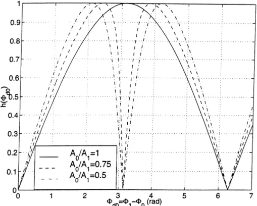
A normalized plot of the envelope voltage for A^jAi = 1, 0.75 and 0.5 is shown in Figure 2.4. Notice that the maximum and minimum value of the output voltage (where the two signals adds constructively and destructivel}'^, respectively) are not 1 and 0 when the losses are unbalanced in the two arms. When the membranes vibrate, the instantenous phase length difference $(/ = <J>i - $ varies around the quiescent value $do· We see that to obtain high sensitivity we should bias $¿0 to the point where the slope of the output is highest.
Note that we should not bias to tt because at that point the slope of the output changes sign, and causes distortion at the output.
2.3
D irect D etectio n
The direct method is based on the fact that narrow band phase-modulation (A4>(.i;(t)) 1) is equivalent to amplitude modulation. Then, we can expand the cosine term in equation 2.5. By approximating cos(A4>(.x(i))) by 1, and sin(A$(a;(i))) by A 4>(3;(t)) we obtain
1 1
Figure 2.4: The normalized plot of the envelope voltage as a function of the phase difference between the two arms of the interferometer.
We can now draw another equivalent model for the detector which is shown in Figure 2.5. Although not a full}' physical one this model is more instructive for the direct detection method.
If we assume a sinusoidal vibration for the membranes such a.sx(t) = a;o+Aa;sin(27r/ii), then the amplitude spectrum of the transmitted signal contains a main signal at the RF frequency and two sidebands that are separated from the main signal with an amount equal to the vibration frequency fi. The sidebands have amplitudes determined by the vibration magnitude of the membranes. Thus, the output is the signal at the sideband which is determined as
— ---·
By inserting A$(:r(t)) of equation 2.4 we get
n2'nfoy/LCoCppo 4.x qCq
Rout =
If we rewrite equation 2.15 in terms of the current, we obtain
T — n f n
J-oxd — -¿TT/o—— nL/ppO----.
4 Xo
(2.15)
(2.16) Now, we can compare the new method with the conventional one by comparing equations 1.1 and 2.16. The DC bias voltage (which is usually in tens of volts range) in the conventional method is replaced by a few volts of RF amplitude in our method. The reduction in voltage magnitude is compensated with the replacement of the vibration frequency f i by the RF frequency /q. Considering a vibration frequency in the MHz range for the membranes, and an RF signal in the GHz range, 1-2 orders of improvement in the sensitivity over the conventional method is possible. For applications which involve lower vibration frequencies (kHz range or lower), the improvement is even higher.
The direct detection is done by down-conversion, and subsequent low-pass filtering of the transmitted signal as shown in Figure 2.6. There is a certain decrease in the output signal because of this down-conversion. The conversion gain of the mixer scales the output given in equations 2.15 and 2.16. The effect of the loss in direct detection is straightforward. The loss in the detector arm Aq scales the output.
If we compare the interferometric method with the direct method by comparing the output expression given in equations 2.10 and 2.15, we see that the two methods are almost equivalent. The difference arises in practical issues. For example, it is not possible to detect very low frequency signals with the direct method, whereas the interferometric method allows even DC measurements.
13
Vf,
in
Figure 2.6: The direct method to measure the phase-modulation.
2.4
S en sitiv ity and th e effect o f th e loss
We have already discussed how the losses are included in the mathematical formula tion. We will now see the sources of the main loss mechanisms, and their effect on the sensitivity of the detection.
We define the sensitivity of the detector as the change in the output voltage AVout for a unit change in the position of the membranes:
V out
S =
Ax (2.17)
For the interferometric detection, using equation 2.13 and $do = $ i — $o we obtain
YfipAi (y4o/^i) sin $do
AW,, = -.A^(x(t)).
2 + {Aq/AiY -I- 2{Aq/Ai) cos$do
Then, inserting equation 2.7 we get the sensitivity for the interferometric detection:
VrfAq sin $¿0 iT'0o Cppo S =
By defining
y / l + {Aq/ AiY -\- 2{Aq/A\) cos $do
sin $do
(2.18)
h{^do) —
y ^ l + {Aq/A]Y -f 2{Aq/A\) cos $¿0
we simplify the sensitivity expression for the interferometric detection. n/?o Cppo
S = VapAoK^do)
4x() Co (2.19)
Equation 2.19 depicts that we have to tune the quiescent phase length difference between the two arms of the interferometer ($do) such that h{i>do) is maximum. Figure 2.7 shows
a plot of h{^do) for three different Aq/ Ai ratio. We see that the maximum value is equal
to 1. When the losses in the two arms are balanced the optimum $do value is equal to 7T. If the loss of the detector arm increases, the maximum h value doesn’t change but the optimum ^do value shifts. In fact, this shift is quite beneficial because we know from Figure 2.4 that we cannot bias $do to tt.
Figure 2.7: The normalized sensitivity as a function of the phase difference between the two arms of the interferometer.
For the direct detection the calculation of the sensitivity is simpler. Using equation 2.15, we get n r „ (2.20) o 1/ A ^ ^ 0 O = VufAq---- · 4xo Co
Notice that, the sensitivity of the direct detection method is identical to that of the interferometric detection for h{^do) = 1·
Equations 2.7 and 2.20 imply that the sensitivity of the detector increases linearly with n. However, this is not the case. Although we have not written explicitly before, the loss of the detector arm Ao is an exponential term like e““", where a is the attenuation constant of the artificial transmission line. By replacing Aq in equations 2.7 and 2.20
15
with e we obtain the actual sensitivity of the detector:
-an^PoCjppQ
(2.21)
4xq Cq
We can view this sensitivity expression as the product of two terms. One of them in creases linearly with n whereas the other one decreases exponentially with n. For small n values the linear term dominates, and for large n values the exponential term dominates. Then, we conclude that there is an optimum number of sections Uopt, beyond which the output starts to decrease with increasing n. The optimum n value is determined by derivating the sensitivity expression with respect to n, which gives
1
(
2.
22)
"^opt — a
The maximum sensitivity obtained for n = riopt is denoted as S„
Po CppO
=-i
Smax — ^RF'. ^
a 4xo Cq (2.23)
The sensitivity is proportional to the RF frequency which is inherent in Po. Therefore, it is better to use higher frequencies. However, the attenuation constant a is frequency dependent. In other words, Uopt and Smax is frequency dependent. There exists an ulti mate optimum in terms of n and /o which can only be determined through simulations.
Both in ordinary and artificial transmission lines the RF loss is unavoidable. Espe cially if one intends to use very high frequencies, the losses must be carefully modeled, and calculated. The main loss mechanism in the artificial transmission lines is the RF resistance of the interconnection lines between the membranes. This ohmic loss is be cause of the finite conductivity of the interconnection lines, and can be modeled as a resistance T2 in series with the inductors as shown in Figure 2.8. Another loss mecha nism is the shunt losses associated with the finite resistivity and the loss tangent of the dielectric. This loss can be modeled as a resistor R\ in parallel with the capacitors. For semi-insulating substrates the ohmic loss is usually the dominant one. Otherwise, both of them are equally effective.
The attenuation constant of a lossy artificial transmission line is derived in Appendix A, and outlined here for convenience:
Za
^2 ,
0/. - -Z-ZT +
L
^2o
— r y T T ^ - A /V
Figure 2.8: A single section lossy artificial transmission line: The lumped element model of a membrane with its interconnections.
For semi-insulating substrates the attenuation constant of equation 2.24 can be simplified to
r2 a =
2Za (2.25)
The T2 and R\ resistances are difficult to calculate. They are very much dependent on the geometry of the device. Furthermore, the parasitic capacitances of the membranes and the interconnection lines, and the parasitic inductance of the membrane electrodes are all very difficult to calculate analytically. Therefore, we use electromagnetic simula tions to obtain the lumped model of a detector section, and predict its performance. We will discuss the electromagnetic simulations thoroughly, but before that we will describe the device fabrication process.
Chapter 3
DEVICE FABRICATION
Although we have mentioned about membranes up to now, the method we introduced can be applied to similar structures as well. The main idea is to integrate the micro- electromechanical device in the form of an artificial transmission line, and use a high frequency RF signals to sense the displacement of the device. The only requirement is that the device must be capacitive so that the displacement of the device results in a change in its capacitance. Therefore, we used air-bridges instead of membranes to test the new method. Actually, an air-bridge and a membrane are equivalent for the detection method. The only difference is in their mechanical properties. There are two thing th at cause the ma.jor variation. One is the material used, and the other one is that a membrane can be sealed leaving vacuum between the membrane and the substrate. On the other hand, in an air-bridge there is air between the bridge and the bottom electrode as the name implies. This may cause a mechanical loading on the air-bridge, and a reduction in the mechanical Q. In spite of these major differences, by properly adjusting their geometry they can be made to have similar properties, at least in air. The reason why we use air-bridges is that it is much easier to fabricate them. Once we see that the method works, it is applicable to any other micro-mechanical device.
The detectors we fabricate consist of a CPW line which is periodically loaded with air-bridges. CPW is a planar transmission media. It consist of signal line which is located between two ground planes. The air-bridges connect the two ground planes, and therefore pass over the signal line. This creates a capacitance between the signal line and the ground which is the capacitive device we need. The lines between the air-bridges
make up the inductors. A section of an artificial transmission line as described above is shown in Figure 3.1. The SEM photograph of a fabricated device is also shown in Figure 3.2.
Figure 3.1: A section of an artificial transmission line with an air-bridge.
Figure 3.2: SEM photograph of an artificial transmission line section with an air-bridge.
3.1
P rocess Steps
We used a standard air-bridge process whose simplified diagram is shown in Figure 3.3. The first step is a metalization step which defines the CPW line. The next step is the
19
sacrificial layer growth which will be removed in the end. The third step is the bridge metalization step. Finally, the sacrificial layer is removed during the lift-off phase of the third step, and the sample is cleaned vuth RIE. There is an additional step which is the pad metalization step. These process steps are explained in detail below.
r
__ B i M
first level metallization
sacrificial layer growth
and patterning
bridge metallization
removal of the sacrificial
layer
j
Figure 3.3: Simplified diagram of an air-bridge process.
In our process we use the following equipment: Karl-Suss mask aligner, Leybold Box Coater and RIE, //Lab PECVD, quartz-type masks which have high UV transmittance, and positive photoresist. The process is quite sensitive to the parameters given below, and most of these parameters are equipment specific. Therefore, the recipe given below may not work with other equipment, and may need tuning.
3.1.1
Normal Lithography L· Metalization
1. P h o to re s is t spinning: After clean ing, the sample surface is covered with photoresist and spinned immediately so that the resist is distributed uniformly over the sample. If the following step is metalization, then it is better to have a thicker photoresist (~ 1.6//m for 3000rpm).
U U U V
u
V3. C h lo ro -b en zo l (o p tio n al): This chemical hardens the photoresist sur face, so that those parts that are not exposed becomes chemically more re sistant to the developer.
2. E x p o su re: The quartz mask is placed over the sample. The regions of the photoresist that are defined by the mask are exposed to UV light of 8mW power for 10 seconds. UV light alters the chemical properties of the photore sist.
4. D ev elo p m en t: The sample is dipped into a certain chemical called developer (AZ400K;l;Water:4). In ~75 second the exposed parts of the photoresist are dis solved (developed) in the developer creating a pattern defined by the mask. Be cause of the diffraction at the edges of the dark regions, those parts that lie under these edges are slightly exposed to UV light as well. During the development pro cess, these regions are also developed creating a smooth edge on the photoresist.
When chloro-benzol is not used, the edges of the photoresist are smooth. As explained in the previous item, chloro-benzol hardens the surface of the photoresist. It protects the unexposed or lightly exposed parts from the devel oper. This results in sharper photore sist edges.
5. M e ta liz a tio n : The sample is coated with metal all over in the Box Coater. The previous exposure and development steps, and the coated metal thickness plays an
important role in the success of the metalization process. When chloro-benzol is not used, there
is a serious lift-off problem, except for very thin metalization (a few thousand
A).
When chloro-benzol is used, the subse quent metalization step is easier. Espe cially, if the coated metal is thin, there is no problem.
When chloro-benzol is used, thick metal coating is possible (over 1pm).
6. Lift-off: After metal coating, the sample is dipped into acetone. Acetone dissolves the photoresist, and lifts off anything above the photoresist. When chloro-benzol is not used, the photoresist edge is very smooth. Thus, the coated metal is like a single piece of metal all over the substrate, and there is a serious lift-off problem.
For a thin metal, there is no problem. The metal over the substrate and over the resist have no connection, so the metal over the resist easily lifts off. For a thick metal, there is a little prob lem. The metal sitting on the substrate and on the photoresist are not totally disconnected. However, the thin con nections easily break up during the lift off leaving overshoots behind.
3.1.2
Image Reversal Lithography and Metalization
Image reversal is a process sequence in which the photo-active properties of the photore sist is reversed. In this way metalization process is less problematic;
1. P h o to re s is t sp inning: It is identical with the normal lithography.
U U V
u
u
y 2. E x p o su re: The quartz mask is placedover the sample. The regions of the _ photoresist that are defined by the mask are exposed to UV light of 8mW power for 6 seconds. Notice that, the mask used in normal lithography, and image reversal are complements. Dark regions on one of them are clear on the other.
3. P o st-e x p o su re bake: After the expo sure, the sample is baked at 110 °C for 2 minutes on a hot-plate.
n'‘l ‘ I ‘ I ‘ ‘
U
u
Vu
U V 4. B lank exposure: The sample is exposed to UV light the second time. However, in this one there is no mask defining dark and clear regions, and the exposure time is 20 seconds.
23
5. D ev elo p m en t: Post-exposure bake and blank exposure sequence reverses the chemical properties of the photoresist. When the sample is dipped into the devel oper, those parts that are not exposed to UV light are developed. Thus, the positive photoresist behaves like a negative photoresist after the image reversal sequence. The diffraction of the UV light from the
edges of the dark regions is still effec tive, but this time it is beneficial. Since dark regions are developed, the pho toresist edges are not smooth an3'^more. Even, there are small balconies at the edges.
1
L I
1
6. M etaliz a tio n ; The sample is coated with metal. Due to the image reversal, the metalization process is mostly very successful.
7. Lift-off: There is almost no problem with the lift-off. Even thick metals are easily lifted off (over 1/im), with no ap parent overshoots at the metal edges.
3.1.3
Sacrificial Layer Growth and Patterning
There are various materials that we can grow as a sacrificial layer using PECVD: SiN, SiO and a-Si. This sacrificial layer will be removed after the bridge metalization. A certain etchant will leak through a narrow spacing, and take away the sacrificial material underneath the bridge. Therefore, the important point is that the material should have a good chemical etchant that does not react with the metalization used.
2. P h o to re s is t spinning: The thickness of the resist is not critical this time, because the following step is an etch step. The role of the resist is to protect the predetermined parts of the sacrifi cial layer from its etchant.
1. Sacrificial layer gro w th : Grow the sacrificial layer using PECVD. The thickness of the sacrificial layer, which is equal to the bridge height, is deter mined by the growth duration. Growth temperature is not very critical for the sacrificial layer, but it is better to keep it low.
u
Vu
'
V
u
Vu
V3. E x p o su re: Normal exposure for 10 seconds at 8 mW UV power.
4. D ev elo p m en t: The sample is dipped into the developer for 75 seconds.
25
5. P o st-b ak e: The sample is baked at ~ 120" for a few minutes to harden the photoresist and make it resistant to the etchant of the sacrificial layer. This is needed because most of the chemicals that are used to etch the sacrificial layer also etches the photoresist. The aim of the post-bake is to make it as resistant as possible.
6. E tch in g : The parts predetermined by the mask are etched away, leaving holes behind. These holes are the posts of the bridges.
7. Photoresist is removed leaving the sac rificial layer. The sacrificial layer haA^'e holes on it which correspond to the bridge pots.
3.1.4
Hard-baked photoresist as a Sacrificial Layer
An alternative to the PECVD grown sacrificial layers is the hard-baked photoresist. Although the dimension control of the photoresist is quite lower with respect to PECVD grown layers, it may be preferred because of its simplicity. Besides, it has a good etchant like Acetone.
1. P h o to re s is t spinning: The spin rate is 5000 rprn, which results in a re sist thickness of 1.4/nn. This sacrificial photoresist is thinned later to the de sired height.
U V
u
Vu
Vu
V2. E x p o su re: We don’t want this sacrifi cial photoresist to lift-off the bridge in later step. Therefore, we over-expose the sample for 10,seconds at 8 mW UV power to obtain smooth edges.
3. D ev elo p m en t: The sample is dipped into the developer for a duration over 75 seconds. That is, we overdevel- ope the sample so that the photoresist edges are smooth.
4. P ost-bake: The sample is baked at ~ 140° for a 25 minutes to harden the photoresist. This hard-bake kills the photo-activity of the photoresist, so that we can make another lithography over this resist.
5. T h in n in g : The sacrificial photoresist is thinned using RIE-Oxygen plasma to the required thickness.
<2 O' O' O'
0" O' O’ O'
3.1.5
Bridge Metalization
Bridge metalization is done either by normal lithography or image reversal which are explained above. However, image reversal is usually preferred.
27
1. P h o to re s is t spinning:
U V
u
Vu
Vu
V2. Image Reversal Sequence: 6 sec onds exposure -I- post-exposure bake at 110 °C for 2 minutes -I- blank exposure for 20 seconds.
3. D ev elo p m en t: 75 seconds of develop ment
4. M etaliz a tio n : The metalization thickness should be thicker than the sacrificial layer height, so that it does not lift-off when removing the sacrificial layer.
5. Lift-oflF an d sacrificial layer re m oval: After the lift-off process, the sample is dipped into the etchant of the sacrificial layer. If hard-baked photore sist is used as a sacrificial layer, then it is readily removed during the lift-off. As a final step of the process it is good to clean the sami)le with oxygen plasma to remove any waste of the whole pro cess.
3.2
P rocess D etails
3.2.1 Mask Design
The masks are designed using a layout editor. In the layout the dark and clear regions of the masks are defined. Each level of the process is governed by a mask. If we consider our process, this means 4 masks including the pad metalization. The layouts of these masks are processed, and put on a single quartz-mask. Thus, a single mask contains several masks which correspond to the different levels of the process. One important point is the alignment of the levels with the previous ones. To simplify the alignment task, alignment marks are put on each level of the process.
3.2.2 Sample cleaning
For the success of the process, and to achieve a high yield sample cleaning is one of the most important issues. For this reason, it is good to apply a three-solvent-cleaning (TCA -f acetone -f isopropanol) at the beginning of each level. There are some exceptions of course. For example, after the sacrificial layer step which uses hard-baked photoresist, we cannot apply three-solvent-cleaning.
Three-solvent cleaning is effective to remove small dust particles from the surface, but there occurs cases in which it is ineffective. Some kind of particles stick to the surface of
29
the sample, and resist to be removed by the three-solvent. For such particles, it is best to use a mechanical cleaning. The most primitive (at the same time probably the most effective) way is to use a Q-tip and wipe the surface with acetone. Another effective way is to use ultrasonics which is not effective for very small particles.
3.2.3
CPW M etalization
The metal used for the CPW metalization which is the first level metalization is not very critical, but it is better if it is the same with the bridge metal. The important thing about the CPW metal is its thickness. The losses discussed in the previous chapter are mostly due to the finite conductivity of the metals. To minimize these ohmic losses we have to use a thick metal (~ l//m). The metal type is also effective, but the two choices A1 and Au have the same conductivities.
Metal coating is done under ultra-high vacuum (in the order of 10“® mbar). The samples to be coated are fixed upside down above a W bolt which contains the metal that will coat the samples. Then, a high current is passed through the boat. As a result, the bolt heats up, and under ultra-high vacuum conditions the metal begins to evaporate. The metal atoms in gas form spread around, and those reaching the sample stick to the sample surface. The metal thickness is determined by the evaporation rate and the coating time.
3.2.4
Sacrificial Layer
The choice of the sacrificial layer is quite trivial. If we choose a PECVD grown material, then we have to find an etchant for it. For example HF etches SiN and Si02 , but does not react with a,-Si. On the other hand, HF etches SiN almost 40 times faster than it etches Si0 2 . Thus, SiN and HF can be a solution. However, if we decide to use a PECVD grown material then we cannot use A1 as a CPW and bridge metal. The reason is that A1 is quite reactive, and dissolves in most of the commonly used etchants like HF. We have to use Au both as CPW and bridge metal. Using Au has some drawbacks as explained in the following subsection.
If we choose to use hard-baked photoresist as the sacrificial la}'er then we loose from dimension control. W hat we gain is a simplified process, and the flexibility to use Al.
Besides we avoid the use of dangerous chemicals like HF.
One big disadvantage of using hard-baked photoresist is that, it is quite thick (~ 1.3^m). It is possible to thin it with RIE, but the result is not very good in terms of uniformity. The etching rate is not constant with time, position on the sample. This results in devices whose bridge heights vary in a range.
3.2.5 Bridge Metalization
The best choice for the bridge metal is Al, for it is a light but strong material. Au is a soft and heavy metal which makes it poor in terms of the mechanical properties. During the sacrificial la}^er removal phase, the surface tension of the liquid pulls the bridges down if we use air drying. To prevent this pull-down we have to employ a critical point drying system [13]. On the other hand, Al bridges are strong enough to oppose the surface tension of the liquid, so the sample can be air dried. Remember th at we can use Al only if we are using hard-baked photoresist as the sacrificial layer, or only if we find an etchant th at does not react with Al.
3.2.6 Pad Metalization
This pad metalization is needed in order to be able to make good contact to the devices on the sample either by microwave probes or by bonding. Therefore, the best choice as a pad metal is Au which is very soft. When used with Ti it sticks to the surface very well making it ideal for probing and bonding. The pad metal should be thicker than 2000 Ain order to be able to make proper contact.
3.3
T he D esigned M asks
We have designed 3 masks to fabricate devices and test them. One of them is a 2- level mask, whereas the others are 4-level. In fact, our process is a 3-level process as described in S(!Ction 3.1. The fourth level included in the latter two corresponds to the pad metalization. It is not recjuired, but increases the probing, bonding and interconnection reliability.