https://doi.org/10.1007/s11468-020-01330-4
An All‑Dielectric Metasurface Coupled with Two‑Dimensional
Semiconductors for Thermally Tunable Ultra‑narrowband Light
Absorption
Ebru Buhara1,2 · Amir Ghobadi1,2 · Ekmel Ozbay1,2,3,4
Received: 10 August 2020 / Accepted: 9 November 2020
© Springer Science+Business Media, LLC, part of Springer Nature 2020
Abstract
Two-dimensional (2D) transition metal dichalcogenides (TMDCs) have attracted tremendous attention over the past decades. Due to their unique features such as high mobility and direct bandgap, they are suitable candidate for the optoelectronic devices. However, due to their ultrathin thickness, their optical absorption is quite weak, and therefore, a trapping scheme for strong light- matter interaction is essential to overcome this deficiency. To accomplish strong light absorption, loss-less dielectric-based metasurfaces with ideally no parasitic absorption are excellent choices. Herein, we report an ultra-narrow-band thermally tunable all-dielectric metasurface coupled absorber with TMD monolayer. In this proposed structure, high absorption with ultra-narrow full-width-at-half-maximum (FWHM) is achieved. Different design configurations are studied to find the most suitable structure. In the optimized design, an absorptance as high as 0.85 with a FWHM of 3.1 nm is achieved. This structure also shows thermal sensitivity of 0.0096 nm/°C, without the use of any phase change material component. This architecture can be used as a 2D and highly efficient tunable single-color photodetector. The proposed dielectric metasurface can be adopted for other types of 2D and ultrathin semiconductor-based optoelectronics.
Keywords Photodetector · Metasurface · Two-dimensional material · Titanium dioxide
Introduction
In recent years, two-dimensional (2D) materials such as gra-phene, hexagonal boron nitride, and transition metal dichal-cogenides (TMDCs) have been attractive research topics due to their exotic electrical, optical, and mechanical properties and their suitability for usage in the future 2D electronic and optoelectronics [1–4]. This interest started after the first
extraction from graphite using the mechanical exfoliation method of graphene, and since then, graphene has become one of the most intensively studied topics in the field of 2D materials [5–8]. Although it attracts tremendous attention and it is used in electronic device development, graphene is an inconvenient substance for digital and optoelectronic applications due to the lack of optical bandgap [9]. This absence caused the focus of the 2D material research to shift to the TMDCs [10–13].
TMDCs are semiconductors in the form of MX2, in which M is a transition metal atom and X is a chalcogen element. The metal atom in the middle bond covalently to the chal-cogen atoms and this bonding constructs a sandwich form in the single layer [14]. Although they have a strong covalent bond in-plane, their out-of-plane bonding is weak due to the van der Waals interactions. Because of that they are able to stay stable, even in the monolayer form [15]. Also, with the help of this weak bonding in out-of-plane, they can be obtained as a monolayer by mechanical exfoliation called as the “Scotch-tape” method [16]. In addition, the synthesis of thin-film TMDCs has been achieved at wafer-scale by
* Ekmel Ozbay [email protected] Ebru Buhara
1 NANOTAM-Nanotechnology Research Center, Bilkent
University, 06800 Ankara, Turkey
2 Department of Electrical and Electronics Engineering,
Bilkent University, 06800 Ankara, Turkey
3 Department of Physics, Bilkent University, 06800 Ankara,
Turkey
4 UNAM-Institute of Materials Science and Nanotechnology,
metal-organic chemical vapor deposition (MOCVD) [17], and small-scale with chemical vapor deposition (CVD) [18].
As a special TMDC semiconductor, monolayer molybde-num disulfide (MoS2) arouse the interest of many
research-ers [19–21]. Similar to other TMDCs, the MoS2 experiences
an indirect to direct bandgap transition (from 1.3 to 1.8 eV) when it turns to monolayer from bulk [22]. Thus, this transi-tion significantly improves photoluminescence and absorp-tion dynamics of the material. Moreover, monolayer MoS2
with a thickness of 0.65 nm has a flexible mechanics due to its high Young’s modulus [23], and it has also high car-rier mobility and high on-off ratio up to 109 [24]. These
properties promise flexible, high-performance, small, and light optoelectronic devices such as ultra-fast detector, field-effect transistors, and photovoltaic cells [25]. Especially high absorption coefficient and bandgap in the visible range makes MoS2 ideal for 2D optoelectronic device applications
[19]. MoS2 gives about 39- and 13-times higher absorption if it is compared with traditional materials such as Si and GaAs in 1-nm layer thickness. Despite its superiority over traditional materials in atomic scale dimension, monolayer MoS2 itself absorbs only ∼ 10% of incident light [26]. Weak absorption due to their extremely thin thickness is the major problem in the way of their use in photoconversion systems. Thus, this 2D semiconductor should be coupled with a trap-ping scheme to increase its light absorption [27].
To be able to enhance this absorption feature of the TMDCs towards the unity, three main trapping schemes can be employed: (i) metal-based plasmonic [28–33], (ii) guided mode resonance [34–37], and (iii) photonic crystal [38–40]-based designs. Although plasmonic structures are common solution to enhance the light-matter interaction in TMDC-based absorbers, metals cause parasitic absorption (Joul loss) due to their larger extinction coefficient (com-pared with that of TMDCs). Thus, the most of the light is consumed in metal parts and absorption efficiency within the TMDC monolayer is low. Moreover, they have large full-width-at-half-maximum (FWHM), due to the fact that the surface plasmon resonances (SPRs) have relatively broad spectral coverage [41]. Guided mode resonance–based designs can provide higher absorption efficiencies (due to their low-loss material nature); however, they have also large FWHM values. Photonic crystal–integrated designs have also bulky nature with multiple fabrication routes, which violates the 2D advantage of these TMDC based designs. Thus, in an ideal scheme, we need to have a lossless and 2D trapping architecture to maximize light coupling into TMDC monolayer. This can be achieved with all-dielectric-based metasurface designs that support the excitation of Mie reso-nances. Dielectric-based designs are lowloss alternatives of metallic designs and have found many applications, in recent years [42–46]. With the help of Mie resonance, the plas-monic effect can be replicated and the lossless characteristic
of the dielectrics can provide a narrow spectral range light confinement, with high absorption efficiency. In addition to these features, the strong light confinement in the dielectric medium can provide high sensitivity into refractive index change. This will provide the opportunity to manipulate the absorption peak response. In other words, this structure can provide thermal tunability without the use of any phase-change material.
In this paper, we propose a dielectric based metasurface platform to achieve ultra-narrowband light absorption within a monolayer thick TMDC layer. For this purpose, we first optimize the metasurface design itself. Then, we couple this design with mono and multilayer TMDCs to observe better absorption results. For this purpose, we choose MoS2, and WS2 as the most commonly used TMDCs. The coupling of
light into Mie resonances, supported by dielectric nanograt-ing, provides narrowband absorption within the TMDC layer. To reach further enhancement, a cavity design is inte-grated into this dielectric-based metasurface. For the best optimized design, the absorptance efficiency reaches to 0.85 and FWHM stays as narrow as 3.1 nm. Finally, we move one step forward to show the thermal tunability characteristic of our design, without use of any phase change material. This is achieved due to strong light confinement within the design. Due to this confinement, any small change in the refractive index is seen by the resonant design. Thus, the resonance frequency shifts and thermal tunability is acquired. The ther-mal sensitivity of the above mentioned optimized design reaches to 0.0096 nm/°C.
Result and Discussion
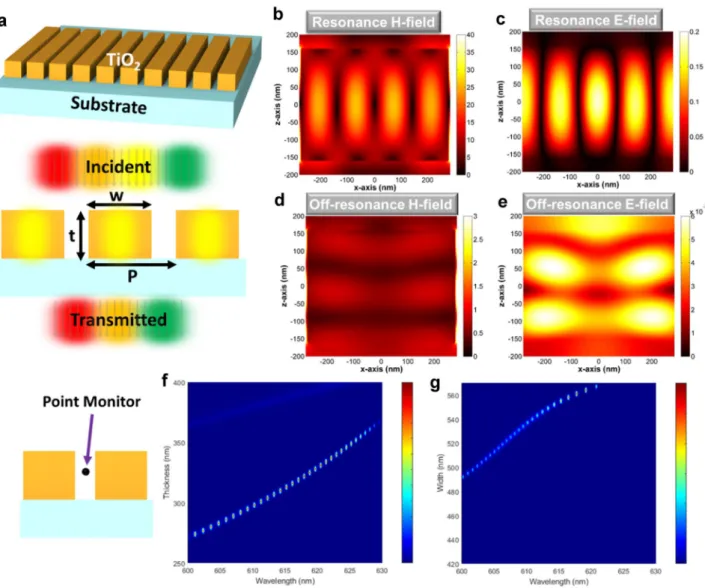
Figure 1 a is a schematic illustration of the dielectric meta-surface design, consisting of nano gratings from titanium dioxide (TiO2). Thickness and width of the TiO2, and the
periodicity of the structure are indicated as t, w, and P, respectfully. The refractive index of TiO2 is set at 2.3705 at room temperature [47]. The calculations to find optimal geometries and dimensions are performed by a commercial finite-difference time-domain (FDTD) software package (Lumerical FDTD Solutions) [48]. While the numerical calculations are executed, the incident light propagation direction is selected as perpendicular to the x-y plane and, boundary conditions for x and y directions are chosen as periodic boundary and perfectly matched layer (PML) for the z direction.
In standard circumstances, TiO2 cannot absorb or
con-fine light due to its transparent and lossless nature in the visible range. Using the proposed design in Fig. 1a, Mie resonances can be excited, and it can provide a spectral selective strong confinement of the light. This strong confinement at the resonance frequency can be seen in
the E-field and H-field profiles across the structure in the Fig. 1b, c. The structure becomes an ordinary transpar-ent dielectric in the off-resonance frequencies, as shown in the Fig. 1d, e. The structure has an ability to provide field enhancement, at specific thickness and width val-ues. For better qualitative comparison, the magnetic field intensities are probed at the point monitor position for the desired spectral range. These filed intensities are studied for different t and W values, while P is kept as 570 nm in all simulations. The sweeping results are shown as a contour plot in the Fig. 1f, g. The contour plots imply that at specific geometrical values the structure provides large absorption cross section. Thus, if a material with high absorption coefficient is embedded into the bottom of the TiO2 grating, spectrally selective light absorption can
be achieved, and the structure becomes an ultra-narrow semiconductor absorber.
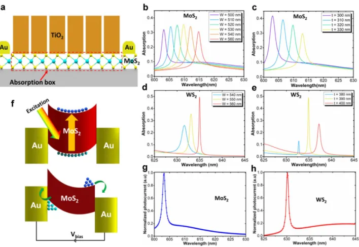
Monolayer TMDCs are excellent candidates for this pur-pose. Due to their single atomic-scale thickness, the off-resonance absorption is quite low and this causes a high-contrast light absorption. MoS2 and WS2 as a monolayer from TMDCs are selected for the absorbent semiconduc-tor layer. In their own case, these monolayer materials can only absorb small amount of the incoming power due to its ultrathin thickness of ~ 0.62 nm. To be able to increase the absorptance magnitude, monolayers are coupled to this resonant metasurface design. This metasurface confines a specific wavelength and passes the rest of spectrum. In other words, it can be seen as an ultra-narrowband band-stop filter.
To examine the absorption features of the structure, MoS2
is placed right underneath the TiO2 nano-grating as a
olayer and absorption measurement is taken on the mon-olayer region. The proposed configuration is shown in the Fig. 2a. Starting with the optimal thickness and width values
Fig. 1 (a) Schematic representation of the proposed dielectric metasurface structure. H-field and E-field distributions across the design for (b, c) resonance frequency and (d, e) off-resonance region. Contour plots of magnetic field intensity dependence to (f) thickness and (g) width
of the metasurface from previous section, the dependence of spectral absorption within the TMDCs to geometrical val-ues is analyzed with 10-nm intervals in Fig. 2b, c. For this purpose, the absorption within the TMDC layer is calculated using below Eq. (1).
This formula has been used to ensure that the absorption is fully within the layer and parasitic absorption is ignored. After finding the optimum dimensions for the width value, which is 530 nm, thickness optimization is performed with final result of 300 nm. For these geometries, the absorption resonance is located at 603 nm wavelength with a maxi-mum absorptance 0.42 and FWHM of 2.7 nm. The same procedure is applied to the WS2 monolayer. The strongest
absorption peak is found at the 560 nm width and 390 nm thickness, as shown in the Fig. 2d, e. The spectral position, amplitude, and FWHM values of this design are 634.9 nm, 0.493, and 0.3 nm. (1) A(𝜆) = 1 Pincident∭ 0.5𝜔imag ( 𝜀 MoS2 ) |E(x, y, z, 𝜆)|2dxdydz
Thus, the function of proposed metasurface is the selective coupling of the incident light into the TMDC semiconductor monolayer. To convert this structure into the photodetector, Au contacts can be made on its surface to form metal-sem-iconductor-metal (MSM) configuration. In this design, upon broadband light illumination, mostly photons corresponding to resonance peak position are absorbed and a photocurrent spectrum similar to absorption profile is achieved. This phe-nomenon is illustrated in the Fig. 2f. COMSOL Multiphysics finite element method solver is used, to numerically analyze the photo-electrical response of the photodetector. As shown in Fig. 2g, h, the proposed design can provide an order of magnitude larger photocurrents in the resonance peak, com-pared with off-resonance ones. Thus, the proposed configura-tion can be utilized to accomplish an ultra-narrowband 2D photodetector.
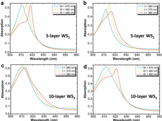
While the absorption peak for both MoS2 and WS2 is quite narrow FWHM, the absorptance amplitude is much below unity. To be able to increase the amplitude towards the unity, two approach can be proposed: (i) increasing the semiconduc-tor layer thickness and (ii) using cavity design to improve light trapping. To examine the first idea, 5-layer, and 10-layer WS2
Fig. 2 (a) Schematic representation of the all-dielectric narrow-band absorber structure, absorption measurement for varying thickness and width of TiO2 with MoS2 (b–c) and WS2 (d–e). (f) The band
align-ment between Au and MoS2 layer before and after applying bias.
The simulated photocurrent values generated by TMD monolayers in (g) MoS2 and (h) WS2 cases
are placed instead of the monolayer. The similar optimization process is conducted to get the highest absorption peak. The results are presented in Fig. 3a, b, c, d. The maximum value is increased up to 0.55 with 5-layer and 0.63 with 10-layer configu-rations. However, this improvement is achieved in the expense of broadening of FWHM (15.1 nm for 5-layer, and 23.1 nm for 10-layer), and increasing the background absorption, compared
with that of monolayer (see Fig. 2d, e). This higher off-reso-nance absorption is the result of thicker semiconductor layer. Thus, in this configuration, although the amplitude has been gradually improved, the selectivity (the ratio of resonance and off-resonance absorptions) is decreased and FWHM is widen. For the second approach, the proposed metasurface design is placed on top of a metal-insulator (MI) cavity. Fig. 4(a) is an
Fig. 3 Absorption measurement for varying (a) thickness and (b) width of TiO2 with 5 Layer
WS2 and varying (c) thickness
and (d) width of TiO2 with 10
Layer WS2
Fig. 4 (a) Proposed optimized cavity design and (b) its absorption profile across the cavity with MoS2 and absorption measurement for varying
illustration of the cavity enhanced design. Silver (Ag) is chosen as the bottom metal mirror. As shown in the absorption per unit volume plot, the dominant part of the absorption occurs within the TMDC monolayer and minor part is lost as parasitic absorp-tion (Jule loss) within the bulk metal. The width and thickness value of TiO2 is optimized in Fig. 4(c) and Fig. 4(d) for MoS2
and Fig. 4(e) and Fig. 4(f) for WS2. The optimal absorption
val-ues are much higher compared to previous designs. For MoS2
case, cavity design has improved absorptance to a value as high as 0.85 with a FWHM of 3.1 nm. While, WS2 cavity design
absorptance value is reached to 0.72 at with a FWHM as nar-row as 1.4 nm.
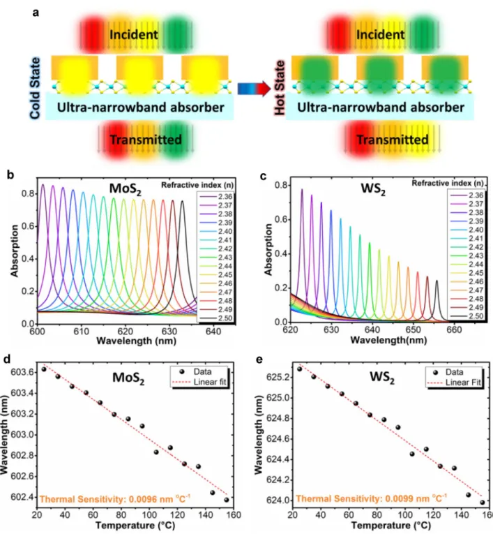
Fig. 5 (a) Schematic illustration of red-shift of the absorption peak as the temperature is increased. Absorption measurement for varying refractive index of TiO2 with (b) MoS2 and (c) WS2 in the proposed
design and thermal sensitivity plots with different temperature for (d) MoS2 and (e) WS2
Besides having high magnetic field enhancement, the structure is also sensitive to the environment temperature. As schematically illustrated in Fig. 5a, the structure has thermally tunable absorption response. This is due to strong field confine-ment within the nanogratings. Changing temperature cause the change in the refractive index of the TiO2 material. Although
TiO2 has very small thermo-optic coefficient of ~ 4.2 × 10⁻⁵ ,
the formation of hot spots in small volume fractions triggers the high sensitivity of the resonance mode into environmental index change. Thus, the change in temperature is resulted with the shift in the absorption spectrum. To show this effect refrac-tive index of TiO2 is swept from 2.36 to 2.5 with 0.01 intervals. This effect is shown with both MoS2 and WS2 material in the Fig. 5a, b. These results are indicated that the design can act as an ultra-narrowband single-color detector, without using any phase change material. The thermal sensitivity graphics of the cavity design for each monolayer are also shown in the Fig. 5d, e. The sensitivity values for MoS2 and WS2-based designs are
0.0096 nm/°C and 0.0099 nm/°C, respectively. These values are significantly high compared with inherent small thermo-optic coefficient of TiO2.
Conclusion
This study is focused to enhance the absorption of TMDCs specifically MoS2 and WS2 monolayer with the help of the
all-dielectric metasurface structure. The absorption behavior of the proposed structure is an ultra-narrowband response over the visible range. The cavity design and multilayer approaches are studied for the further enhancement of the absorptance amplitude. The cavity approach was shown to be a promising approach to maximize the performance of the design. Due to strong field confinement, the proposed design revealed ther-mally tunable absorption response, without the use of phase-change component. This paper proposes a universal design approach that can be used in other 2D and ultrathin optical systems where strong and selective light absorption can be achieved in atomic scale dimensions. The tunability added to this design provides the opportunity to realize multi-color pho-todetectors using the same design. As temperature changes, the absorption peak experiences a spectral shift and by this way we can detect different colors using the same photodetector design. Besides, this design has the ability to be used in sens-ing application as well. As an unknown agent is coated on the grating surface, the resonance peak will shift, and from the produced shift value, one can estimate the refractive index of the material.
Authors’ Contributions First author (E.B.) carried out design, tion, and analysis of the results. Second author (A.G.) helped in simula-tion and discussion steps of the paper. Last author (E.O.) supervised the study. All the authors contributed in the paper writing.
Compliance with Ethical Standards
Competing Interests The authors declare that they have no competing interests.
References
1. Wang QH, Kalantar-Zadeh K, Kis A et al (2012) Electronics and optoelectronics of two-dimensional transition metal dichalco-genides. Nat Nanotechnol 7:699
2. Novoselov KS, Jiang D, Schedin F, Booth TJ, Khotkevich VV, Morozov SV, Geim AK (2005) Two-dimensional atomic crys-tals. Proc Natl Acad Sci USA 102:10451
3. Neto AHC, Novoselov K (2011) Two-dimensional crystals: beyond graphene. Mater Express 1:10
4. Dean C, Young A, Meric I (2010) Boron nitride substrates for high-quality graphene electronics. Nature Nanotech 5:722–726 5. Novoselov KS, Geim AK, Morozov SV, Jiang D, Zhang Y,
Dubonos SV, Grigorieva IV, Firsov AA (2004) Electric field effect in atomically thin carbon films. Sci 306:666–669 6. Schwierz F (2010) Graphene transistors. Nature Nanotech
5:487–496
7. Grigorenko A, Polini M, Novoselov K (2012) Graphene plas-monics. Nature Photon 6:749–758
8. Xia F, Mueller T, Lin Y et al (2009) Ultrafast graphene photo-detector. Nature Nanotech 4:839–843
9. Novoselov K, Fal′ko V, Colombo L (2012) A roadmap for gra-phene. Nature 490:192–200
10. Peng B, Kailian Ang P, Loh KP (2015) Two-dimensional dichal-cogenides for light-harvesting applications. Nano Today 10(2) 11. Li H, Shi Y, Chiu MH, Li LJ (2015) Emerging energy applica-tions of two-dimensional layered transition metal dichalcoge-nides. Nano Energy 18
12. Li Z, Wong SL (2017) Functionalization of 2D transition metal dichalcogenides for biomedical applications. Mater Sci Eng C 70 Part 2
13. McDonnell SJ, Wallace RM (2016) Atomically-thin layered films for device applications based upon 2D TMDC materials. Thin Solid Films Volume 616
14. Pech-Canul MI, Ravindra NM (2019) Semiconductors: synthe-sis, properties and applications. Springer
15. Geim A, Grigorieva I (2013) Van der Waals heterostructures. Nature 499:419–425
16. Li H, Wu J, Yin Z, Zhang H (2014) Preparation and applications of mechanically exfoliated single-layer and multilayer MoS2 and WSe2 nanosheets. Acc Chem Res 47:1067–1075
17. Kang K, Xie S, Huang L (2015) High-mobility three-atom-thick semiconducting films with wafer-scale homogeneity. Nature 520:656–660
18. Chhowalla M, Shin H, Eda G (2013) The chemistry of two-dimen-sional layered transition metal dichalcogenide nanosheets. Nature Chem 5:263–275
19. Xia F, Wang H, Xiao D (2014) Two-dimensional material nano-photonics. Nature Photon 8:899–907
20. Wu S, Buckley S, Schaibley J (2015) Monolayer semiconductor nanocavity lasers with ultralow thresholds. Nature 520:69–72 21. Xue Y, Zhang Y, Liu Y, Liu H, Song J et al (2016) Scalable
pro-duction of a few-layer MoS2/WS2 vertical heterojunction array and
its application for photodetectors. ACS Nano 10(1):573–580 22. Lee HS, Min S-W, Chang Y-G, Park MK, Nam T, Kim H, Kim
JH, Ryu S, Im S (2012) MoS2Nanosheet Phototransistors with Thickness-Modulated Optical Energy Gap. Nano Lett 12:3695
23. Akinwande D, Petrone N, Hone J (2014) Two-dimensional flexible nanoelectronics. Nat Commun 5:5678
24. Radisavljevic B, Radenovic A, Brivio J, Giacometti V, Kis A (2011) Single-layer MoS2 transistors. Nat Nanotechnol 6:147
25. Xie C, Yan F (2017) Flexible photodetectors based on novel func-tional materials. Small 13:1701822
26. Bernardi M, Palummo M, Grossman JC (2013) Extraordinary sun-light absorption and one nanometer thick photovoltaics using two-dimensional monolayer materials. Nano Lett 13(8):3664–3670 27. Ghobadi A, Ulusoy Ghobadi TG, Karadas F, Ozbay E (2019)
Semiconductor thin film based metasurfaces and metamaterials for photovoltaic and photoelectrochemical water splitting applica-tions. Adv Opt Mater 7:1900028
28. Chen W, Wang L, Jiang Y, Wang J (2018) A perfect absorber based on monolayer MoS2 and nano-silver in the visible regime,
2018 International Conference on Microwave and Millimeter Wave Technology (ICMMT). Chengdu 1–3
29. Huo D, Zhang J, Wang H (2017) Broadband perfect absorber with monolayer MoS2 and hexagonal titanium nitride nano-disk array.
Nanoscale Res Lett 12:465
30. Bahauddin SM, Robatjazi H, Thomann I (2016) Broadband absorption engineering to enhance light absorption in monolayer MoS2. ACS Photonics 3(5):853–862
31. Zhou K, Song J, Lu L, Luo Z, Cheng Q (2016) Plasmon-enhanced broadband absorption of MoS2-based structure using Au
nanopar-ticles. Opt Express 27(3):2305–2316
32. Song J, Lu L, Cheng Q, Luo Z (2018) Surface plasmon-enhanced optical absorption in monolayer MoS2 with one-dimensional Au
grating. J Quant Spectrosc Radiat Transf
33. Butun S, Palacios E, Cain JD, Liu Z, Dravid VP, Aydin K (2017) Quantifying plasmon-enhanced light absorption in monolayer WS2 films. ACS Appl Mater Interfaces 9(17):15044–15051
34. Jiang X, Wang T, Xiao S, Yan X, Cheng L, Zhong Q (2018) Approaching perfect absorption of monolayer molybdenum disulfide at visible wavelengths using critical coupling. Nano-technol. 29(33):335205
35. Fang X, Tian Q, Yang G (2019) Enhanced absorption of mon-olayer molybdenum disulfide (MoS2) using nanostructures with symmetrical cross resonator in the visible ranges. Opt. Quant Electron 51:21
36. Sr JH, Ren Y, Qing Y, Li H, Yao E, Wu X, Liu W, Xie W (2018) Dual-band total absorption via guided-mode resonance in a mon-olayer MoS2 covered dielectric grating structure, Proc. SPIE
10823. Nanophotonics and Micro/Nano Optics IV 108230T
37. Qing YM, Ma HF, Yu S, Cui TJ (2019) Ultra-narrowband absorp-tion enhancement in monolayer transiabsorp-tion-metal dichalcogenides with simple guided-mode resonance filters. J Appl Phys 125:21 38. Nong J, Da H, Fang Q, Yu Y, Yan X (2018) Perfect absorption in
transition metal dichalcogenides-based dielectric grating. J Phys D: Appl Phys 51:375105
39. Liu JT, Wang TB, Li XJ, Liu NH (2014) Enhanced absorption of monolayer MoS2 with resonant back reflector. J Appl Phys 115:19
40. Lu H, Gan X, Mao D, Fan Y, Yang D, Zhao J (2017) Nearly perfect absorption of light in monolayer molybdenum disulfide supported by multilayer structures. Opt Express 25:21630–21636 41. Ghobadi A, Hajian H, Butun B, Ozbay E (2018) Strong light-matter interaction in lithography-free planar metamaterial perfect absorbers. ACS Photonics 5(11):4203–4221
42. Yildirim DU, Ghobadi A, Soydan MC, Serebryannikov AE, Ozbay E (2020) One-way and absolute polarization insensitive near-perfect absorption by using an all-dielectric metasurface. Opt Lett OL 45(7):2010–2013
43. Yildirim DU Ghobadi A Ozbay E (2018) Near-absolute polari-zation insensitivity in graphene based ultra-narrowband perfect visible light absorber. Sci Rep 8(1)
44. Yildirim DU et al (2019a) Colorimetric and near-absolute polarization-insensitive refractive-index sensing in all-dielec-tric guided-mode resonance based metasurface. J Phys Chem C 123(31):19125–19134
45. Yildirim DU et al (2019b) Disordered and densely packed ITO nanorods as an excellent lithography-free optical solar reflector metasurface. ACS Photonics 6(7):1812–1822
46. Soydan MC, Ghobadi A, Yildirim DU, Erturk VB, Ozbay E (2019) All Ceramic-based metal-free ultra-broadband perfect absorber. Plasmonics 14(6):1801–1815
47. Saleem MR, Honkanen S, Turunen J (2014) Thermal properties of TiO2 films fabricated by atomic layer deposition. IOP Conf Ser
Mater Sci Eng
48. Lumerical Solutions, Inc. http://www.lumer ical.com/tcad-produ cts/ fdtd/
Publisher’s Note Springer Nature remains neutral with regard to jurisdictional claims in published maps and institutional affiliations.