GaN-on-SiC LNA for UHF and L-Band
Salahuddin Zafar
#*1, Sinan Osmanoglu
#*2, Busra Cankaya
#*3, AhsanUllah Kashif
†4, Ekmel Ozbay
#*5 #Nanotechnology Research Center (NANOTAM), Turkey*Department of Electrical and Electronics Engineering, I.D. Bilkent University, Turkey †Department of Electrical Engineering, IIUI, Pakistan
{1zafar, 2sinano, 3bcankaya}@ee.bilkent.edu.tr, 4[email protected], 5[email protected]
Abstract — In this paper, we report a broadband GaN HEMT
LNA from 100 MHz to 2 GHz, using common source with inductive degeneration and RC feedback topology. Flat gain response of ±1.5 dB variation for 9 V drain voltage with 108 mA drain current bias is achieved. Noise characteristics for frequencies as low as 100 MHz have been explored for the first time for GaN-on-SiC technology. A gain greater than 8 dB with single stage, and promising values of input reflection coefficient (smaller than -8.9 dB) and output reflection coefficient (smaller than -7.1 dB) have been achieved, respectively. Minimum NF of 2.9 dB is achieved while an NF smaller than 5 dB is reported in the usable frequency range from 310 MHz to 2 GHz. Performance evaluation is also done for both low and high drain current and voltage values. In-house 0.15 µm GaN-on-SiC process is used to design this MMIC. The chip size for designed MMIC is 1.35 mm x 1.35 mm.
Keywords — broadband, flat gain, low-noise amplifier, UHF,
L-band, Gallium Nitride, HEMT, SiC I. INTRODUCTION
GaN HEMT technology has emerged as a replacement of GaAs for many applications. High Electron Mobility Transistors (HEMTs) having high saturated drain current density along with no intentional doping achieve very high mobility of electrons in the channel. Moreover, GaN, being a wideband semiconductor, has a high breakdown electric field. Therefore, HEMTs based on GaN technology have the best combination of power handling capability and speed. The issue of low thermal conductivity of GaN material has already been improved by growing GaN epitaxial layers on SiC substrate to compensate for high power density and realize GaN RF power transistors [1], [2].
The initial focus of research for GaN HEMT technology was power amplification for GaN HEMT technology, but it is desirable to use the same technology for both transmit and receive MMICs to design low cost, compact, and efficient single chip transceiver modules. GaN HEMTs not only provide a comparable noise figure (NF) with GaAs and other InP based technologies, but also have built-in capability to handle high power at the receive end. Therefore, designing of GaN based low noise amplifiers (LNAs) removes the need of a protection circuit at the input and simplifies the transceiver design [2], [3]. A lot of research and efforts have been made to take the full advantage of GaN RF transistors by exploiting their power capabilities for power as well as low noise amplification. However, when it comes to the frequencies below S-band,
although efforts are still undergoing for power amplification, very little attention has been paid to GaN HEMT based LNA design. Some power amplifiers have recently been reported in UHF and L-band for their applications in radar, nano-satellite GPS, space, tactical ground, and air communication as well as their potential use in commercial wireless and broadband public safety communication networks [4]–[8]. On the other hand, there have been very few GaN based LNA designs covering UHF and L-band in full or partially. A 0.2-8 GHz GaN MMIC LNA-PA has been reported with characteristics of low noise as well as power amplification. However, noise performance is evaluated for frequencies greater than 1 GHz [9]. S. Piotrowicz et al. presented a two-stage flat gain L-band robust LNA for receiver front-end modules based on GaN technology [10]. Y. Yamaguchi demonstrated a broadband LNA from 600 MHz to 6 GHz using distributed amplifier configuration with active gate termination, aiming to utilize the white space via frequency sensing system [11]. In another attempt, LNA design simulated using Cree packaged transistor from 1 GHz to 6 GHz has been reported for WiMax applications [12].
As discussed earlier, using the same GaN HEMT technology for both transmit and receive sections is the need of the hour, and there is much room available to explore the performance of LNAs in UHF and L-band. Therefore, we focused our attention to design a broadband LNA from 100 MHz to 2 GHz with a gain variation of less than ±1.5 dB in the band. LNA is designed using 0.15 µm GaN-on-SiC HEMT technology with RC feedback and source degeneration topology. Common source (CS) topology, combined with series degeneration inductor, provides good linearity and improvement in noise properties [3], [9]. As the CS topology has bandwidth-gain trade-off due to miller effect [13], RC feedback is used to achieve the stable broadband response.
II. FABRICATION AND DESIGN
AlGaN/GaN HEMT on SiC process of Bilkent University Nanotechnology Research Center (NANOTAM) is used for the design and fabrication of LNA MMIC. Active devices and passive elements are fabricated on a 3-inch SiC substrate which is grown by metal-organic chemical vapor deposition (MOCVD). The fabrication starts with mesa isolation etching by plasma-based dry etch process. Ohmic contacts are formed as Ti/Al/Ni/Au metal stacks using electron beam evaporation. Gates of active devices are deposited by electron beam
Proceedings of the 1st European Microwave Conference in Central Europe
lithography to achieve a T-shaped gate with 150 nm foot length. The sample is passivated with a SixNy layer using plasma-enhanced chemical vapor deposition. TaN thin film resistor layer is deposited by sputtering to achieve 30 Ohms/□ resistance. The process has two metallization layers. MIM capacitors have capacitance density of 250 pF/mm2. The air bridge post structure is constituted between the metal layers. In the back-side processing, SiC layer is thinned to 100 µm and back-side via-holes are coated with Au to introduce ground layer.
Fig. 1 shows the simplified schematic of our proposed broadband LNA. The size of designed MMIC is only 1.35 mm x 1.35 mm. It is packaged and then mounted on the PCB. The photograph of fabricated MMIC along with its implementation on PCB is shown in Fig. 2. Due to low frequency operation of MMIC, large bias inductors for gate and drain (Ld and Lg) could not be realized using the aforementioned process. Therefore, packaged MMIC was mounted on a PCB to perform the measurements by introducing external bias inductors. HEMT is fabricated with series source degeneration to make the modelling unerring. CS topology is used along with RC feedback to achieve flat broadband response. This RC feedback provides input and output matching as well as the stability with stability network at the output. Electromagnetic (EM) simulations were performed to observe the realistic results before the fabrication.
Fig. 1. Simplified schematic of GaN HEMT LNA
Fig. 2. Photograph of designed MMIC and its implementation on a PCB
III. RESULTS AND DISCUSSION
EM simulations resulted in flat gain response from 0.1 GHz to 2 GHz with a gain variation of ±1.3 dB and an NF less than 1.8 dB throughout the band. In the simulations, overall gain was greater than 9.5 dB while input reflection coefficient (IRC) and output reflection coefficient (ORC) were better than -8.3 dB and -7.9 dB, respectively. Stability was achieved for all simulation range. Fig. 3 shows the measurement and simulation results where a good match is achieved for S-parameters from 0.1 GHz to 2 GHz. For the fabricated device, maximum gain of 11.3 dB is attained at 430 MHz and it remained above 8.4 dB from 100 MHz to 2 GHz. Reflection coefficients are better than -8.9 dB and -7.1 dB ensuring a good input and output matching, respectively.
Fig. 3. S-parameters measurement results of fabricated GaN-on-SiC MMIC at bias of 9 V, 108 mA along with the simulation results
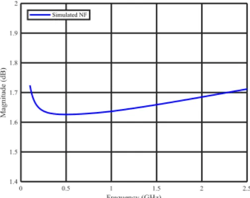
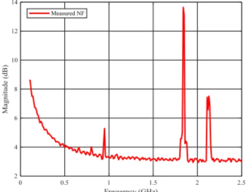
The simulated NF can be seen in Fig. 4, while the measured NF is in Fig. 5. NF of less than 4 dB is achieved for frequencies greater than 540 MHz . NF remains between 4 dB and 5 dB for frequencies from 310 MHz to 540 MHz, while the lowest value of NF is 2.9 dB at 1.95 GHz. These results show that the designed MMIC is realized to have a usable bandwidth in UHF range and L-band. This is for the first time, to the best of our knowledge, that noise properties of broadband GaN LNA up to 2 GHz have been explored to as low as 100 MHz frequency. Although the measurement results for NF are not in a perfect match with the simulation results, the fabricated MMIC is still considerable for RF front-end applications from 310 MHz to 2 GHz. The large bandwidth with an NF less than 5 dB using CS topology has been reported for the first time for GaN LNAs, to the best of our knowledge.
Fig. 4. Noise figure simulation results of LNA MMIC
Two parameters need explanation in context to NF measurements. First point is that the deviation of results for the fabricated MMIC is due to the variations in the process, changing the transistor model slightly. Furthermore, the noise data used for design below 0.9 GHz was not directly from measurements but from noise model developed by one of the authors (S.O.). Process variations caused different leakage values compared to the used transistor model, and resulted with higher NF for low frequencies. This situation ultimately makes a room of improvement for the process parameters. Second point is that some peaks are observed in the NF measurement data which are due to the adjacent channel devices operating in the same band and mobile communication bands.
Fig. 5. Measured noise figure of fabricated MMIC at bias of 9V, 108mA
Performance of the fabricated MMIC is tested for different bias points and the results are summarized in Fig. 6. It has been observed that the device performs better for higher bias current in terms of IRC, gain, and NF. Performance results for ORC and gain variation are better for low bias points. IRC better than -8.5 dB and gain greater than 8.2 dB were achieved for bias points of 9 V, 90 mA and 9 V, 108 mA. For 9 V, 45 mA, ORC as low as -7.4 dB and gain variation of only ±1.3 dB are attained. Noise figure less than 5 dB was measured from 330 MHz and 310 MHz to 2 GHz, for 9 V, 90 mA and 9 V, 108 mA, respectively. The lowest value of NF of 2.9 dB at 1.9 GHz for 9 V, 90 mA was measured. The overall best noise performance is achieved for 9 V, 108 mA. To conclude with, the device performance for higher bias current proves to be promising with a very little compromise over output match and gain variation.
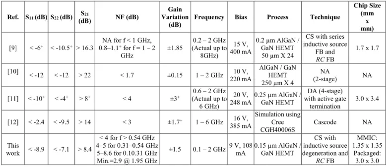
Comparative analysis of our proposed LNA with already published data is summarized in Table-1. As explained earlier, there have not been many efforts to explore the broadband response of GaN LNAs for frequencies as low as 100 MHz, especially in terms of NF. Even the designs referred in Table-1 with broadband response in UHF range have reported NF above 500 MHz. Y. Yamaguchi et. al reported an NF less than 4 dB from 0.6 GHz to 2 GHz with a decent gain of greater than 8 dB [11]. Our design achieved the same NF for the frequency starting from 540 MHz with the similar gain and better ORC. We realized a compact chip size owing to single stage CS topology instead of distributed amplifier or cascode design. Although distributed amplifier topology provides the widest bandwidth, CS topology is better in terms of noise performance
[3]. Gain variation of ±1.5 dB, achieved in this work, is the best reported value for GaN-on-SiC LNAs in the frequency range from 0.1 GHZ to 2 GHz. Moreover, this work has competitive performance parameters in L-band having only one stage and chip size as small as 1.35 mm x 1.35 mm, which increases to 3.0 mm x 3.0 mm with the package.
Fig. 6. S-parameters and NF measurements data for different bias points from 300 MHz to 2 GHz
Table 1. Comparative analysis with recently published data (+Estimated values from figure, NA=Not Available, CS=Common Source, DA=Distributed Amplifier,
FB=Feedback)
IV. CONCLUSION
A broadband common source LNA has been realized using 0.15 µm GaN HEMT technology. Flat gain of ±1.5 dB variation and NF less than 5 dB with promising input and output reflection coefficient values provide the best ever reported combination for CS GaN MMIC LNAs in the frequency band from 310 MHz to 2 GHz, to the best of our knowledge. Moreover, noise properties being explored for the first time in the lower band of frequencies paves a way for related future exploration and designs for applications in the fields of radar, GPS, space, tactical ground, and air communication.
ACKNOWLEDGMENT
The authors would like to acknowledge the efforts and workmanship of NANOTAM fabrication team for the device and MMIC fabrication.
REFERENCES
[1] M. Rudolph, "GaN HEMTs for low-noise amplification — status and challenges," 2017 Integrated Nonlinear Microwave and
Millimetre-wave Circuits Workshop (INMMiC), Graz, 2017, pp. 1-4.
[2] R. Caverly et al., "Advancements at the Lower End: Advances in HF, VHF, and UHF Systems and Technology," in IEEE Microwave
Magazine, vol. 16, no. 1, pp. 28-49, Feb. 2015.
[3] K.W. Kobayashi and Mike Wojtowicz, “GaN Low Noise Broadband Amplifiers and Technology”, 2012. [Online]. Available: http://citeseerx.ist.psu.edu/viewdoc/download?doi=10.1.1.364.6164&re p=rep1&type=pdf [Jan. 20, 2019].
[4] H. Liu and Y. Jiang, "UHF-Band 4kW Broadband High Efficiency GaN Amplifier," 2018 International Conference on Microwave and
Millimeter Wave Technology (ICMMT), Chengdu, 2018, pp. 1-3.
[5] H. Wu, K. S. Yuk, C. Cui, and G. R. Branner, "High power class F GaN HEMT power amplifier in L band for global positioning systems application," 2018 IEEE 19th Wireless and Microwave Technology
Conference (WAMICON), Sand Key, FL, 2018, pp. 1-4.
[6] L. Yuchao, Z. Shichang, and L. Wei, "Design of a Broadband GaN Power Amplifier," 2018 International Conference on Microwave and
Millimeter Wave Technology (ICMMT), Chengdu, 2018, pp. 1-3.
[7] B. Dou, J. Yan, Y. Wu, L. Wang, C. Lv, and X. Wang, "High-Performance and Low-Cost L-Band T/R Module for Space Application,"
2018 International Conference on Microwave and Millimeter Wave Technology (ICMMT), Chengdu, 2018, pp. 1-3.
[8] A. Raza and J. Gengler, "Design of a 70 W wideband GaN HEMT power amplifier with 60% efficiency over 100–1000 MHz bandwidth," 2018
IEEE Topical Conference on RF/Microwave Power Amplifiers for Radio and Wireless Applications (PAWR), Anaheim, CA, 2018, pp. 72-74.
[9] K. W. Kobayashi, Y. Chen, I. Smorchkova, R. Tsai, M. Wojtowicz, and A. Oki, "A 2 Watt, Sub-dB Noise Figure GaN MMIC LNA-PA Amplifier with Multi-octave Bandwidth from 0.2-8 GHz," 2007
IEEE/MTT-S International Microwave Symposium, Honolulu, HI, 2007,
pp. 619-622.
[10] S. Piotrowicz et al., "Broadband AlGaN/GaN high power amplifiers, robust LNAs, and power switches in L-Band," 2009 European
Microwave Integrated Circuits Conference (EuMIC), Rome, 2009, pp.
431-434.
[11] Y. Yamaguchi, T. Kaho, M. Kawashima, H. Shiba, and T. Nakagawa, "A wideband GaN low noise amplifier for a frequency sensing system,"
2014 Asia-Pacific Microwave Conference, Sendai, Japan, 2014, pp.
420-422.
[12] A. M. Bassal and A. H. Jarndal, "GaN low noise amplifier design for WiMax applications," 2016 16th Mediterranean Microwave Symposium
(MMS), Abu Dhabi, 2016, pp. 1-4.
[13] Lecture 23 - Frequency Response of Amplifiers (I) Common-Source Amplifier [online] Available: https://ocw.mit.edu/courses/electrical- engineering-and-computer-science/6-012-microelectronic-devices-and-circuits-fall-2005/lecture-notes/lecture23annotat.pdf
Ref. S11 (dB) S22 (dB) (dB) S21 NF (dB) Variation Gain (dB)
Frequency Bias Process Technique
Chip Size (mm x mm) [9] < -6+ < -10.5+ > 16.3 0.8–1.1NA for f < 1 GHz, + for f = 1 – 2 GHz ±1.85 0.2 – 2 GHz (Actual up to 8GHz) 15 V, 400 mA 0.2 µm AlGaN / GaN HEMT 50 µm X 24 CS with series inductive source FB and RC FB 1.7 x 1.7 [10] < -12 < -12 > 22 < 1.7 ±0.15 1 – 2 GHz 10 V, 220 mA AlGaN / GaN HEMT 250 µm X 4 NA (2-stage) NA [11] < -10+ < -4+ > 8+ < 4 ±3+ (Actual up to 0.6 – 2 GHz 6 GHz) 20 V, 248 mA 0.25 µm AlGaN / GaN HEMT DA (4-stage) with active gate
termination 3.0 x 3.4 [12] < -2.4 < -9.5 > 14 < 3 ±1.7+ 1 – 6 GHz 16 V, 385 mA Simulation using Cree CGH40006S Cascode NA This work < -8.9 < -7.1 > 8.4 < 4 for f > 0.54 GHz 4–5 for 0.31–0.54 GHz 5–8.6 for 0.10.31 GHz Min.=2.9 @ 1.95 GHz
±1.5 0.1 – 2 GHz 9 V, 108 mA 0.15 µm AlGaN / GaN HEMT
CS with inductive source degeneration and RC FB MMIC: 1.35 x 1.35 Packaged: 3.0 x 3.0