The effect of AlN interlayer thicknesses on
scattering processes in lattice-matched AlInN/GaN
two-dimensional electron gas heterostructures
To cite this article: A Teke et al 2009 New J. Phys. 11 063031
View the article online for updates and enhancements.
Related content
Mobility limiting scattering mechanisms in nitride-based two-dimensional
heterostructures
S Gökden, R Tülek, A Teke et al.
-Simulation study on electrical
characteristic of AlGaN/GaN high electron mobility transistors with AlN spacer layer Niraj Man Shrestha, Yiming Li and Edward Yi Chang
-Growth parameter investigation of AlGaN/GaN/AlN's with Hall measurements S B Lisesivdin, S Demirezen, M D Caliskan et al.
-Recent citations
Unintentional incorporation of Ga in the nominal AlN spacer of AlInGaN/AlN/GaN Heterostructure
Shujun Dai et al
-Probing the Local Electrical Properties of Al(In,Ga)N by Kelvin Probe Force Microscopy
Albert Minj et al
-Optimization of Graded AlInN/AlN/GaN HEMT Device Performance Based on Quaternary Back Barrier for High Power Application
Sharidya Rahman et al
-T h e o p e n – a c c e s s j o u r n a l f o r p h y s i c s
New Journal of Physics
The effect of AlN interlayer thicknesses on scattering
processes in lattice-matched AlInN/GaN
two-dimensional electron gas heterostructures
A Teke1,5, S Gökden1, R Tülek1, J H Leach2, Q Fan2, J Xie2, Ü Özgür2, H Morkoç2, S B Lisesivdin3 and E Özbay3,41Department of Physics, Faculty of Science and Letters, Balıkesir University, Ça˘gı¸s Kampüsü, 10145 Balıkesir, Turkey 2Department of Electrical and Computer Engineering, Virginia Commonwealth University, Richmond, VA 23284, USA
3Nanotechnology Research Center-NANOTAM, Bilkent University, 06800 Ankara, Turkey
4Department of Physics, Department of Electrical and Electronics Engineering, Bilkent University, 06800 Ankara, Turkey
E-mail:[email protected]
New Journal of Physics11 (2009) 063031 (12pp)
Received 17 March 2009 Published 16 June 2009 Online athttp://www.njp.org/
doi:10.1088/1367-2630/11/6/063031
Abstract. The scattering mechanisms governing the transport properties
of high mobility AlInN/AlN/GaN two-dimensional electron gas (2DEG) heterostructures with various AIN spacer layer thicknesses from zero to 2 nm were presented. The major scattering processes including acoustic and optical phonons, ionized impurity, interface roughness, dislocation and alloy disorder were applied to the temperature-dependent mobility data. It was found that scattering due mainly to alloy disorder limits the electron mobility for samples having spacer layer thicknesses up to 0.3 nm. On the other hand, alloy scattering is greatly reduced as the AlN spacer layer thickness increases further, and hence the combination of acoustic, optical and interface roughness become operative with different degrees of effectiveness over different temperature ranges. The room-temperature electron mobility was observed to increase gradually as the AlN spacer layer increases. A peak electron mobility of 1630 cm2V−1s−1 was realized for the sample consisting of a 1 nm AlN spacer layer. Then, 5Author to whom any correspondence should be addressed.
the electron mobility decreased for the sample with 2 nm AlN. Moreover, the measured 2DEG densities were also compared with the theoretical predictions, which include both piezoelectric and spontaneous polarization components existing at AlN/GaN interfaces. The experimental sheet carrier densities for all AlInN/AlN/GaN HEMT structures were found to be in excellent agreement with the theoretical predictions when the parasitic (unintentional) GaN layer deposited between AlN and AlInN was taken into account. From these analyses, 1 nm AlN spacer layer thickness is found to be the optimum thickness required for high electron mobility and hence low sheet resistance once the sheet carrier density is increased to the theoretically expected value for the sample without unintentional GaN layer.
Contents
1. Introduction 2
2. Experimental details 3
3. Experimental results and calculations 3
4. Conclusions 11
Acknowledgments 12
References 12
1. Introduction
Al(In)GaN/(In)GaN-based high electron mobility transistors (HEMTs) have attracted a great deal of attention for high-frequency and high-power microwave applications because nitride-based material systems have desirable fundamental physical properties, such as a large band gap, large breakdown field and strong spontaneous and piezoelectric polarization fields [1]. To improve the performance of devices, various barrier and channel alternatives have been used in nitride-based HEMTs [2]–[8]. Several achievements have been made by optimizing the growth and design parameters. For example, the introduction of a thin AlN spacer layer at the AlGaN/GaN interface increases the carrier density and effectively reduces the alloy scattering of two-dimensional electron gas (2DEG) as well as provides better carrier confinement [7, 9]. AlGaN/GaN-based HEMTs are designed with a trade-off between a high electron mobility (µe), typically 1600 cm2V−1s−1, and a high-sheet carrier density (ns), typically 1.5 × 1013cm−2, providing a two-dimensional (2D) sheet resistance Rs, typically 250 sq−1 [10].
In recent years, AlInN barrier layer has been implemented instead of AlGaN to improve the HEMT performance after the original proposal of Kuzmík [11]. The advantage of using an AlInN barrier is to adjust the composition of the alloys to obtain a lattice- or polarization-matched heterostructure. When the indium (In) composition is set to about 18%, the alloy and GaN are lattice-matched. The polarization charge is, therefore, completely determined by spontaneous polarization, since the structure is free of strain. The HEMTs with an AlInN barrier layer were essentially predicted to provide higher carrier densities than those with an AlGaN barrier layer [12]. Once the mobility of the former is achieved at the same level with that of the latter, the conductivity performance of the AlInN-based devices would be higher, promising
for high-power and high-frequency transistor operations [13]. Gonschorek et al reported a room-temperature Hall mobility value of 1170 cm2V−1s−1 along with 2.6 × 1013cm−2 2DEG density for an undoped nearly lattice-matched AlInN/AlN/GaN heterostructure having various AlN interlayer thicknesses [5]. Similary, Xie et al [4] reported the effect of the AlN spacer layer on the transport properties of AlInN/AlN/GaN HEMTs and observed that samples with 1.1 nm AlN spacer thicknesses exhibit the highest room-temperature Hall mobility value of 1550 cm2V−1s−1 with sheet carrier density 9 × 1012cm−2. Despite these successful results reported in the literature, there are only a few reports in terms of the detailed analysis of the transport characteristics of AlInN-based HEMTs [5,13,14].
In the present work, we investigate the transport properties of high-quality AlInN/AlN/GaN heterostructures with different AlN interlayer thicknesses using temperature-dependent Hall effect measurements. Analytical models were applied to the experimental data in order to understand scattering mechanisms that govern the transport properties of devices in a temperature range of 10–300 K. If the scattering mechanisms that are dominant for high-density 2DEGs can be identified, it will guide the modifications to the growth and/or the layer structure that will be necessary to further improve the conductivity. This work has emphasized that about 1 nm AlN spacer layer thickness is an optimum spacer thickness required for high electron mobility in AlInN/AlN/GaN heterostructures.
2. Experimental details
Al0.82In0.18N/AlN/GaN HEMT structures were grown on 2 inch (0001) sapphire substrates in a vertical low-pressure metal–organic chemical vapor deposition (MOCVD) system. For all HEMT structures, the growth was initiated with the deposition of a 400 nm AlN buffer layer grown at ∼1020◦C, followed by an 2.2 µm thick nominally undoped GaN layer grown at ∼960◦C. Over these templates, 0.3, 1 and 2 nm thick high-temperature AlN spacer layers were grown. As a reference, one sample was grown without an AlN spacer layer. After the deposition of spacer layers, the wafer was cooled down to ∼800◦C for the growth of Si-doped AlInN barrier layer with a thickness of ∼16 nm (AlInN barrier layer is unintentionally doped for the sample with no spacer layer). The indium content in the AlInN barrier is kept around 18%, close to perfect lattice matching to GaN. Finally, the growth was finished with a 3 nm thick GaN cap layer. As the carrier gas, hydrogen was used for the growth of the AlN and GaN layers, and nitrogen for AlInN. Additionally, we have discovered from transmission electron microscopy (TEM) analysis that there is a thin (2–3 nm) unwanted GaN layer on top of the AlN spacer due to residual Ga in the chamber during growth. The samples with no spacer and, 0.3, 1 and 2 nm AlN spacer thicknesses will be referred to as samples A, B, C and D, respectively, from now on. After growth, the samples were characterized by high resolution x-ray diffraction (HRXRD), atomic force microscopy (AFM) and variable temperature Hall measurements.
3. Experimental results and calculations
HRXRD measurements were performed to determine the overall structural quality and the alloy compositions of four samples. X-ray data were collected on the (0002) reflections with ω–2θ scans. Figure 1 shows ω–2θ scan XRD patterns around the (0002) reflection for AlInN/AlN/GaN samples exhibiting increasing AlN interlayer thickness. The structural quality
Figure 1. HRXRD (0002) ω–2θ scans of Al0.82In0.18N/AlN/GaN heterostruc-tures with increasing AlN spacer layer thicknesses (samples A–D). The curves are shifted for clarity.
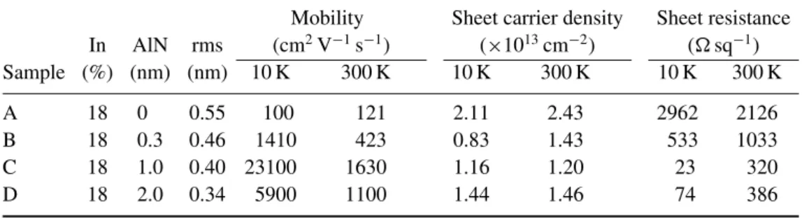
Table 1. Summary of the main structural parameters such as In content and
AlN spacer layer thickness and characterization results: AFM rms, Hall mobility, sheet carrier density, sheet resistance at low and room temperature.
Mobility Sheet carrier density Sheet resistance In AlN rms (cm2V−1s−1) (×1013cm−2) ( sq−1) Sample (%) (nm) (nm) 10 K 300 K 10 K 300 K 10 K 300 K A 18 0 0.55 100 121 2.11 2.43 2962 2126 B 18 0.3 0.46 1410 423 0.83 1.43 533 1033 C 18 1.0 0.40 23100 1630 1.16 1.20 23 320 D 18 2.0 0.34 5900 1100 1.44 1.46 74 386
of the samples were revealed by Pendellösung fringes, clearly resolved in HRXRD curves. The well-resolved diffraction peaks (or shoulders) related to AlInN barrier layers are observed at around 17.5◦. In addition, no phase separation was evident in the HRXRD data, which indicates that the AlInN layers were grown coherently on the AlN/GaN structures. From the relative XRD peak positions and by using the lattice constants of GaN, AlN and InN given in table 1
and Vegard’s law, the In compositions in AlInN were determined to be around 18% for all samples. The actual In composition is still somewhat debatable due the deviation from Vegard’s law reported in literature [15]. However, such variation in In content of AlInN barrier layers would not violate the arguments made on the transport properties of the studied four samples.
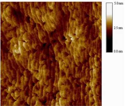
Figure 2 shows a typical AFM image of an AlInN/AlN/GaN sample with a 2 nm AlN spacer layer. The surface morphology is similar in other samples. Since the surface is strongly affected by the surface of the underlayers, the root mean square (rms) roughness values
Figure 2. 5 × 5 µm2 AFM image of sample D with a 2 nm AlN spacer layer thickness. The rms roughness is 0.34 nm.
obtained from AFM scans listed in table 1 could mimic one of the interface parameters used in the theoretical calculation of mobility limited by interface roughness scattering. The surface becomes slightly smoother (from ∼0.55 to ∼0.34 nm) as the thickness of the AlN interlayer increases.
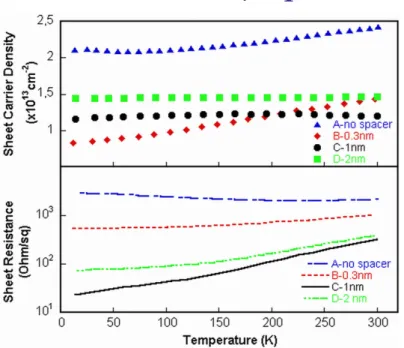
Temperature-dependent Hall measurements were carried out from 10 to 300 K using a van der Pauw geometry in a LakeShore Hall measurement system. Ohmic contacts were prepared by 60 s rapid thermal annealing of Ti/Al/Ti/Au (30/100/30/30 nm) at 850◦C. Figure3shows the temperature-dependent Hall sheet carrier density and 2D sheet resistance for all lattice-matched Al0.82In0.18N/AlN/GaN HEMT structures. As seen in the figure, the sheet carrier densities for samples C and D remain nearly constant through the studied temperature ranges. This temperature behavior of sheet carrier densities implies that the conduction is dominated almost exclusively by the carriers at the AlN/GaN heterointerfaces. On the other hand, sheet carrier densities of samples A and B increase monotonically as the temperature increases, probably due to the temperature-induced thermal excitation of impurities in bulk GaN and AlInN [16]. In the same figure, the temperature dependences of corresponding 2D sheet resistances are also shown. Temperature dependences of 2D sheet resistances for samples C and D are determined by their temperature-dependent mobility, which decreases as the temperature increases, as will be discussed later. On the other hand, sheet resistance is less temperature-dependent due to opposite temperature character of sheet carrier densities and mobilities for samples A and B. The corresponding sheet carrier densities and sheet resistances values at low and room temperature are listed in table1. The minimum room-temperature sheet resistance is obtained as 320 sq−1 (corresponding sheet carrier density and mobility are 1.2 × 1013cm−2 and 1630 cm2V−1s−1, respectively) for sample C with 1 nm AlN spacer layer. Although the mobility is one of the highest mobility values reported, sheet resistance is not low enough since the sheet carrier density in our sample is much lower than the theoretically expected value.
Figure 3. The temperature dependence of measured sheet carrier density and sheet resistance for all samples.
Table 2. The constants used for the calculation of the polarization and sheet
carrier density in AlInN/AlN/GaN heterostructures.
AlN GaN InN
PSP(C m−2) −0.081 −0.029 −0.032 e33(C m−2) 1.46 0.73 0.97 e31(C m−2) −0.60 −0.49 −0.57 C13(GPa) 108 103 92 C33(GPa) 373 405 224 a0(Å) 3.112 3.189 3.540
To calculate the 2D sheet carrier concentrations from the polarization induced sheet charge densities and compare them with the observed sheet charge densities in our lattice-matched AlInN/AlN/GaN HEMTs, the theory presented by Ambacher et al [8] and Asbeck et al [17] has been pursued. The constants used in our calculations were taken from Bernardini et al [18] and Wright [19] and are given in table 2. Figure 4 shows the calculated maximum sheet electron densities ns(x) as a function of In composition that exist at the AlN/GaN interface of the AlInN/AlN/GaN HEMT structures along with the experimental data obtained from Hall measurements. In these calculations, the effect of the AlN spacer layer, GaN cap layer and parasitic GaN layer were taken into account. The calculated sheet carrier densities were in excellent agreement with the experimental values for all samples.
It is here that we will discuss the temperature-dependent Hall mobilities for all samples along with the results of the theoretical model. The model accounts for the major scattering mechanisms such as optical phonon, acoustic phonon, through both deformation potential and piezoelectric, interface roughness, background impurity, dislocation and alloy disorder. The details of the calculations are given in [20] and references therein. The parameters used in these
Figure 4.Composition dependence of the maximum sheet carrier concentration of the 2DEG confined at AlxIn1−xN/AlN/GaN interfaces including GaN cap layer and AlN spacer layer. For comparison, the experimental sheet carrier densities obtained by Hall measurement at room temperature are also indicated.
Table 3.Values of GaN material constants used in the calculation of scattering mechanisms.
Electron effective mass(m0) m∗= 0.22 High-frequency dielectric constant(ε0) ε∞= 5.35 Static dielectric constant(ε0) εs= 8.9 LO-phonon energy(meV) ¯hω = 92 Longitudinal acoustic phonon velocity(m s−1) υ
L= 6.56 × 10³ Density of the crystal(kg m−3) ρ = 6.15 × 10³ Deformation potential(eV) ED= 8.3
Elastic constants(N m−2) cLA= 2.65 × 10¹¹, cTA= 0.442 × 10¹¹ Electromechanical coupling coefficient K2= 0.039
Electron wave vector(m−1) k = 7.27 × 10⁸
Effective Bohr radius in the material(Å) aB= 23.1 Lattice constant in the (0001) direction(Å) c0= 5.185 2D Thomas Fermi wave vector(m−1) qTF= 8.68 × 10⁸
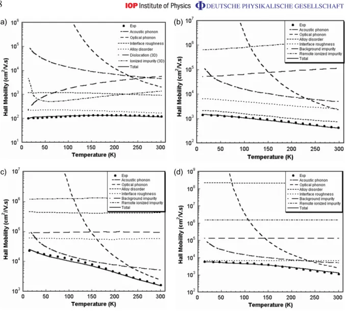
calculations are taken from [1] and tabulated in table 3. In these calculations, the temperature dependence of the sheet carrier densities was also considered. The results are shown in figure5
For sample A, where the AlN spacer layer is not used, the Hall mobility at room temperature is extremely low, 120 cm2V−1s−1, with a high sheet carrier density of 2.43 × 1013cm−2, which is similar to that reported by other groups [5, 21]. Around 190 K, the Hall mobility reaches its maximum and decreases to 100 cm2V−1s−1 at 10 K (see figure 5(a)). The temperature-dependent Hall mobility revealed that the conduction in this sample is mainly determined by alloy disorder scattering at moderate and high temperatures. Alloy disorder is indeed very high
(a) (b)
(c) (d)
Figure 5. The temperature evolution of the measured Hall mobility in
comparison with the theoretical calculations including major scattering mechanisms for (a) sample A, (b) sample B, (c) sample C and (d) sample D.
in InAlN, as a 350 meV photoluminescence linewidth with a Stokes shift over 500 meV in In0.18Al0.82N alloys has been observed [14]. On the other hand, Hall mobility deviates from the value limited by alloy scattering at low temperatures. Since the temperature behavior of Hall mobility at low temperatures mimics the bulk type of transport we included 3D ionized impurity and dislocation scattering mechanisms. Very good agreement is revealed through whole temperature ranges as seen in figure 5(a). Hence, it can be argued that the transport in this sample is determined by a combination of 2D and 3D scattering processes.
When the AlN spacer layer is introduced between the AlInN and GaN interface, the Hall mobility dramatically improved depending on the thickness of the AlN due to very efficient reduction in alloy disorder scattering. Indeed the incorporation of only a 0.3 nm thick AlN interlayer at the AlInN/GaN interface (sample B) immediately improved the room temperature mobility to 432 cm2V−1s−1, which is more than four times higher than the sample with no spacer layer as seen in figure 5(b). However, the mobility is still mainly limited by the
alloy disordering, and to a lesser extent to interface roughness scattering through the whole temperature range.
As the thickness of AlN spacer layer is increased to about 1 nm (sample C) the Hall mobility is obtained as 1630 cm2V−1s−1 at room temperature and reaches 23 100 cm2V−1s−1 at low temperature due to more effective suppression of alloy scattering as seen in figure5(c). The calculated total mobility as a function of the lattice temperature is in very good agreement with the experimental data. As seen in the figure, high-temperature (T>240 K) mobility is determined by both acoustic and polar optical phonons scattering with increasing strength of the optical phonons component as the temperature increases to room temperature. At moderate temperature ranges, the acoustic phonon scattering through both deformation potential and piezoelectric interactions with nearly equal strength dominates the Hall mobility. As the temperature decreases further, the mobility is characterized by the combination of three scattering mechanisms, namely background impurity, interface roughness and acoustic phonon. Therefore, the low field transport in sample C is assumed to be nearly intrinsic. The weaknesses of extrinsic scattering mechanisms assure the realization of a high-quality GaN channel with a low dislocation density and a smooth interface.
The temperature dependence of Hall mobility for sample D with a 2 nm-thick AlN spacer layer is fairly different from that of sample C as is seen in figure 5(d). The measured Hall mobility is reduced to 1100 cm2V−1s−1 at room temperature and reaches 5900 cm2V−1s−1 at low temperature. Although the scattering by alloy disorder is still effectively suppressed, the mobility is now nearly determined by other extrinsic mechanisms, interface roughness at low temperatures and acoustic phonon at moderate temperatures. Above 200 K, acoustic and optical phonons along with the interface roughness scattering became effective in the determination of the mobility. The strength of the optical phonon component increases as the temperature reaches room temperature. This indicates that the interface between AlN and GaN becomes poorer as the thickness of AlN spacer layer increases beyond 1 nm as will be discussed later.
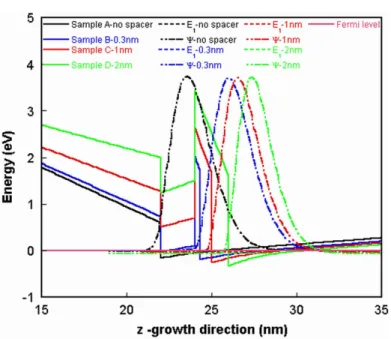
Let us now discuss the effect of the AlN spacer layer on transport characteristics of our AlInN/AlN/GaN HEMT structures in some detail. Inserting an AlN spacer layer between lattice-matched AlInN and GaN effectively changes the transport properties of the AlInN/AlN/GaN heterostructures, especially for the suppression of the scattering due to alloy disorder. Figure6shows the conduction and valance potential profiles and spatial distribution of the amplitude of the electron wavefunctions calculated by solving 1D nonlinear self-consistent Schrödinger–Poisson equation [22]. The material parameters of AlInN for simulation were deduced using Vegard’s law and layers were assumed to be as pseudomorphically grown. As seen in the figure the spatial variation of the electron wavefunctions, particularly their penetration into the barrier, gradually decreases as the AlN spacer layer increases due to higher band offset of AlN. Keeping the carriers in the channel away from the scattering centers results in a significant increase in the Hall mobility as discussed above. The unavoidable (intrinsic) scattering mechanisms associated with acoustic and optical phonons are mostly influenced by charge carrier density, effective well width at the heterointerface and position of the Fermi level. As seen in figure 6, the pseudo-triangular potential well becomes deeper and hence the effective well width becomes narrower as the AlN spacer layer increases. In the calculation of the mobility limited by phonon scattering, we used the effective potential well widths deduced from the full width at half-maximum of the electron wavefunctions. Therefore, optical phonon scattering, which mainly determines the room temperature mobility of the sample with thicker AlN spacer, is more pronounced and reaches the lowest value of 1800 cm2V−1s−1for sample D.
Figure 6. The calculated conduction and valence potential profiles and spatial distribution of the amplitude of the electron wavefunctions for all samples.
As will also be noted from the calculated potential profiles, the band edges of the parasitic quantum wells resulting from the unwanted GaN layer between AlN and AlInN layers are well above the Fermi level, which excludes any accumulation of carriers in this channel and hence the possibility of parallel transport for samples C and D. Therefore, the arguments made on the transport properties of samples A, C and D by considering only single channel existing between AlN and GaN are valid. However, for sample B, since the Fermi level is close to the conduction band edge of the parasitic GaN quantum well (its thickness, which is not known exactly, determines the position of the band edge with respect to the Fermi level) parallel conduction could be possible.
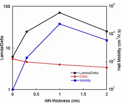
More interestingly, the effect of the AlN spacer layer on the measured Hall mobility at low temperature where the interface roughness scattering is more effective is not clear. In general, there are two parameters used in the calculation of the mobility limited purely by interface roughness scattering, namely the correlation length 3 and lateral size 1 at the AlN/GaN interface, respectively. In the calculation, the rms roughness values obtained from AFM scans were taken as the lateral size parameter. The correlation length was taken in the range of 50–250 nm [23] as a free parameter to fit the experimental mobility data. The mobility increases as1 decreases and 3 increases. Therefore, we plotted Delta, Lambda/Delta (3/1) and low-temperature mobility as a function of AlN spacer layer thickness, as shown in figure 7. In this calculation, the effect of the sheet carrier density on shifting the centroid of the electron distribution towards the interface on the effectiveness of the interface roughness scattering [24] was also taken into account. As seen 3/1, the larger the value of which the smoother the interface, increases as the AlN spacer layer increases up to 1 nm, and then it decreases again as the AlN spacer layer increases further. However, it should be noted here that the delta parameter obtained experimentally from rms values of AFM images decreases slightly as the AlN spacer increases. Gonschorek et al have reported the effect of AlN spacer layer on electron mobilities in AlInN/GaN HEMT structures, and found that the thickness of
Figure 7. 1, 3/1 and low-temperature mobility as a function of AlN spacer
layer thickness.
the spacer can dramatically influence the surface morphology and can result in the variation of the mobility [5]. However, opposite to their results, where surface morphology deteriorates as the AlN spacer layers increase, the surface morphology of our AlInN/AlN/GaN HEMTs is slightly improved or at least nearly unchanged by increasing the AlN spacer layer as far as the average roughness (rms ∼= 1) in growth direction is concerned. When the average lateral roughness (λ or 3/1) deduced from the mobility analysis is considered, the AlN spacer layer improves the channel/barrier interface. This helps to reduce the alloy and the interface roughness scattering, which results in higher electron mobility. On the other hand, when the AlN interlayer thicknesses exceed a critical value of about 1 nm, Lambda/Delta decreases again due to probably increased partial strain relaxation, which deteriorates the interface, resulting in decreased Hall mobility in the channel. This is in good agreement with investigations on AlInN/AlN/GaN HEMTs [4, 5] as well as AlGaN/AlN/GaN HEMTs, where an optimal AlN spacer layer thickness of ∼1 nm is also reported [7,9].
4. Conclusions
We studied the transport properties of lattice-matched AlInN/AlN/GaN heterostructures with various AlN spacer layer thicknesses by using temperature-dependent Hall measurements. The scattering mechanisms were successfully analyzed and the dominant scattering mechanisms in the low- and high-temperature regimes were determined for all heterostructures. It was found that the AlN spacer layer is a crucial growth parameter that must be considered in HEMT design based on lattice-matched AlInN/GaN heterostructures. From the analysis of the scattering mechanisms governing the transport properties and the AFM images of our samples, we concluded that the AlN interlayer greatly helps to reduce the alloy and the interface roughness scattering, which results in a higher mobility, but on the other hand, it should not exceed a optimal value of ∼1 nm to avoid structural degradation, resulting in decreased Hall mobility. As for the sheet resistance, we obtained the lowest sheet resistance value of 320 sq−1
for sample C with the optimal AlN spacer layer. This can be reduced further once the sheet carrier density is increased to a theoretically expected value of 2.4 × 1013cm−2at the AlN/GaN interface for the sample without parasitic GaN layer. In this particular scenario, where only the intrinsic scattering mechanisms are effective, we would expect to have a 2D sheet resistance of only about 160 sq−1.
Acknowledgments
The VCU portion of this work has been funded by a grant from the US Air Force Office of Scientific Research under the direction of Drs Kitt Reinhardt and Don Silversmith. The NANOTAM portion of this work is supported by TUBITAK under project numbers 104E090, 105E066, 105A005, 106E198 and 106A017 and the European Union under the projects EU-METAMORPHOSE, EU-PHOREMOST, EU-PHOME and EU-ECONAM. One of us (EO) acknowledges partial support from the Turkish Academy of Sciences.
References
[1] Morkoç H 2008 Handbook of Nitride Semiconductors and Devices vols I–III (New York: Wiley) [2] Xie J, Leach J H, Ni X, Wu M, Shimada R, Özgür Ü and Morkoç H 2007 Appl. Phys. Lett.91 262102
[3] Miyoshi M, Egawa T, Ishikawa H, Asai K-I, Shibata T, Tanaka M and Oda O 2005 J. Appl. Phys.98 063713
[4] Xie J, Ni X, Wu M, Leach J H, Özgür Ü and Morkoç H 2007 Appl. Phys. Lett.91 132116
[5] Gonschorek M, Carlin J-F, Feltin E, Py M A and Grandjean N 2006 Appl. Phys. Lett.89 062106
[6] Lisesivdin S B, Acar S, Kasap M, Ozcelik S, Gokden S and Ozbay E 2007 Semicond. Sci. Technol.22 543
[7] Smorchkova I P, Chen L, Mates T, Shen L, Heikman S, Moran B, Keller S, DenBaars S P, Speck J S and Mishra U K 2001 J. Appl. Phys.90 3998
[8] Ambacher O et al 1999 J. Appl. Phys.85 3222
[9] Cao Y and Jena D 2007 Appl. Phys. Lett.90 182112
[10] Palacios T, Rajan S, Chakraborty A, Heikman S, Keller S, DenBaars S P and Mishra U K 2005 IEEE Trans.
Electron Devices52 2117
[11] Kuzmík J 2001 IEEE Electron Device Lett.22 510
[12] Kuzmík J 2002 Semicond. Sci. Technol.17 540
[13] Tulek R, Ilgaz A, Gokden S, Teke A, Ozturk M K, Kasap M, Ozcelik S, Arslan E and Ozbay E 2009 J. Appl.
Phys.105 013707
[14] Butté R et al 2007 J. Phys. D: Appl. Phys.40 6328
[15] Hums C, Bläsing J, Dadgar A, Diez A, Hempel T, Christen J, Krost A, Lorenz K and Alves E 2007 Appl.
Phys. Lett.90 022105
[16] Lisesivdin S B, Yildiz A, Acar S, Kasap M, Ozcelik S and Ozbay E 2007 Appl. Phys. Lett.91 102113
[17] Asbeck P M, Yu E T, Lau S S, Sullivan G J, van Hove J and Redwing J 1997 Electron. Lett.33 1230
[18] Bernardini F, Fiorentini V and Vanderbilt D 1997 Phys. Rev. B56 R10024
[19] Wright A F 1997 J. Appl. Phys.82 2833
[20] Gokden S, Baran R, Balkan N and Mazzucato S 2004 Physica E24 249
Gokden S, Ilgaz A, Balkan N and Mazzucato S 2004 Physica E25 86
[21] Dadgar A, Schulze F, Bläsing J, Diez A, Krost A, Neuburger M, Kohn E, Daumiller I and Kunze M 2004
Appl. Phys. Lett.85 5400
[22] Birner S, Hackenbuchner S, Sabathil M, Zandler G, Majewski J A, Andlauer T, Zibold T, Morschl R, Trellaki A and Vogl P 2006 Acta Phys. Pol. A 110 111
[23] Çörekçi S, Usanmaz D, Tekeli Z, Çakmak M, Özçelik S and Özbay E 2008 J. Nanosci. Nanotechnol.8 640