On the mechanisms of InGaN electron cooler in
InGaN/GaN light-emitting diodes
Zi-Hui Zhang,1 Wei Liu,1 Swee Tiam Tan,1 Zhengang Ju,1 Yun Ji,1 Zabu Kyaw,1 Xueliang Zhang,1 Namig Hasanov,1 Binbin Zhu,1 Shunpeng Lu,1 Yiping Zhang,1 Xiao
Wei Sun,1,3 and Hilmi Volkan Demir1,2,*
1LUMINOUS! Centre of Excellence for Semiconductor Lighting and Displays, School of Electrical and Electronic Engineering, Nanyang Technological University, 50 Nanyang Avenue, 639798, Singapore
2Department of Electrical and Electronics, Department of Physics, and UNAM-Institute of Material Science and Nanotechnology, Bilkent University, TR-06800, Ankara, Turkey
3[email protected] *[email protected]
Abstract: Electron overflow limits the quantum efficiency of InGaN/GaN light-emitting diodes. InGaN electron cooler (EC) can be inserted before growing InGaN/GaN multiple quantum wells (MQWs) to reduce electron overflow. However, detailed mechanisms of how the InGaN EC contributes to the efficiency improvement have remained unclear so far. In this work, we theoretically propose and experimentally demonstrate an electron mean-free-path model, which reveals the InGaN EC reduces the electron mean free path in MQWs, increases the electron capture rate and also reduces the valence band barrier heights of the MQWs, in turn promoting the hole transport into MQWs.
©2014 Optical Society of America
OCIS codes: (230.3670) Light-emitting diodes; (230.5590) Quantum-well, wire, and-dot devices; (160.6000) Semiconductor materials.
References and links
1. S. T. Tan, X. W. Sun, H. V. Demir, and S. P. DenBaars, “Advances in the LED materials and architectures for energy-saving solid-state lighting toward ‘lighting revolution’,” IEEE Photon. J. 4(2), 613–619 (2012). 2. S. Pimputkar, J. S. Speck, S. P. DenBaars, and S. Nakamura, “Prospects for LED lighting,” Nat. Photonics 3(4),
180–182 (2009).
3. Z.-H. Zhang, S. T. Tan, Z. G. Ju, W. Liu, Y. Ji, Z. Kyaw, Y. Dikme, X. W. Sun, and H. V. Demir, “On the effect of step-dDoped quantum barriers in InGaN/GaN light emitting diodes,” J. Disp. Technol. 9(4), 226–233 (2013). 4. Z.-H. Zhang, S. T. Tan, W. Liu, Z. G. Ju, K. Zheng, Z. Kyaw, Y. Ji, N. Hasanov, X. W. Sun, and H. V. Demir,
“Improved InGaN/GaN light-emitting diodes with a p-GaN/n-GaN/p-GaN/n-GaN/p-GaN current-spreading layer,” Opt. Express 21(4), 4958–4969 (2013).
5. Z.-H. Zhang, S. T. Tan, Z. Kyaw, Y. Ji, W. Liu, Z. Ju, N. Hasanov, X. W. Sun, and H. V. Demir, “InGaN/GaN light-emitting diode with a polarization tunnel junction,” Appl. Phys. Lett. 102(19), 193508 (2013).
6. Y. Ji, Z.-H. Zhang, S. T. Tan, Z. G. Ju, Z. Kyaw, N. Hasanov, W. Liu, X. W. Sun, and H. V. Demir, “Enhanced hole transport in InGaN/GaN multiple quantum well light-emitting diodes with a p-type doped quantum barrier,” Opt. Lett. 38(2), 202–204 (2013).
7. M.-H. Kim, M. F. Schubert, Q. Dai, J. K. Kim, E. F. Schubert, J. Piprek, and Y. Park, “Origin of efficiency droop in GaN-based light-emitting diodes,” Appl. Phys. Lett. 91(18), 183507 (2007).
8. H. Zhao, G. Liu, R. A. Arif, and N. Tansu, “Current injection efficiency induced efficiency-droop in InGaN quantum well light-emitting diodes,” Solid-State Electron. 54(10), 1119–1124 (2010).
9. Z.-H. Zhang, S. T. Tan, Y. Ji, W. Liu, Z. G. Ju, Z. Kyaw, X. W. Sun, and H. V. Demir, “A PN-type quantum barrier for InGaN/GaN light emitting diodes,” Opt. Express 21(13), 15676–15685 (2013).
10. E. Kioupakis, P. Rinke, K. T. Delaney, and C. G. Van de Walle, “Indirect Auger recombination as a cause of efficiency droop in nitride light-emitting diodes,” Appl. Phys. Lett. 98(16), 161107 (2011).
11. X. Ni, X. Li, J. Lee, S. Liu, V. Avrutin, U. Ozgur, H. Morkoc, and A. Matulionis, “Hot electron effects on efficiency degradation in InGaN light emitting diodes and designs to mitigate them,” J. Appl. Phys. 108(3), 033112 (2010).
12. X. Ni, X. Li, J. Lee, S. Liu, V. Avrutin, U. Ozgur, H. Morkoc, A. Matulionis, T. Paskova, G. Mulholland, and K. R. Evans, “InGaN staircase electron injector for reduction of electron overflow in InGaN light emitting diodes,” Appl. Phys. Lett. 97(3), 031110 (2010).
13. S. H. Park, Y. T. Moon, D. S. Han, J. S. Park, M. S. Oh, and D. Ahn, “High-efficiency InGaN/GaN light-emitting diodes with electron injector,” Semicond. Sci. Technol. 27(11), 115003 (2012).
14. C.-H. Jang, J.-K. Sheu, C. M. Tsai, S.-J. Chang, W.-C. Lai, M.-L. Lee, T. K. Ko, C. F. Shen, and S. C. Shei, “Improved performance of GaN-based blue LEDs with the InGaN insertion layer between the MQW active layer and the n-GaN cladding layer,” IEEE J. Quantum Electron. 46(4), 513–517 (2010).
15. J. K. Sheu, G. C. Chi, and M. J. Jou, “Enhanced output power in an InGaN-GaN multiquantum-well light-emitting diode with an InGaN current-spreading layer,” IEEE Photon. Technol. Lett. 13(11), 1164–1166 (2001). 16. K. T. Tsen, R. P. Joshi, D. K. Ferry, A. Botchkarev, B. Sverdlov, A. Salvador, and H. Morkoc, “Nonequilibrium
electron distributions and phonon dynamics in wurtzite GaN,” Appl. Phys. Lett. 68(21), 2990–2992 (1996). 17. Y. T. Rebane, Y. G. Shreter, B. S. Yavich, V. E. Bougrov, S. I. Stepanov, and W. N. Wang, “Light emitting
diode with charge asymmetric resonance tunneling,” Phys. Status Solidi A 180(1), 121–126 (2000).
18. D. Saguatti, L. Bidinelli, G. Verzellesi, M. Meneghini, G. Meneghesso, E. Zanoni, R. Butendeich, and B. Hahn, “Investigation of efficiency-droop mechanisms in multi-quantum-well InGaN/GaN blue light-emitting diodes,” IEEE Trans. Electron. Dev. 59(5), 1402–1409 (2012).
19. H. Zhao, G. Liu, J. Zhang, R. A. Arif, and N. Tansu, “Analysis of internal quantum efficiency and current injection efficiency in III-nitride light-emitting diodes,” J. Disp. Technol. 9(4), 212–225 (2013).
20. C. S. Xia, Z. Q. Li, S. Yang, L. W. Cheng, W. D. Hu, and W. Lu, “Simulation of InGaN/GaN light-emitting diodes with a non-local quantum well transport model,” 12th International Conference on Numerical Simulation of Optoelectronic Devices (NUSOD), 21–22(2012).
21. V. Fiorentini, F. Bernardini, and O. Ambacher, “Evidence for nonlinear macroscopic polarization in III–V nitride alloy heterostructures,” Appl. Phys. Lett. 80(7), 1204–1206 (2002).
22. J. Piprek, “Efficiency droop in nitride-based light-emitting diodes,” Phys. Status Solidi A 207(10), 2217–2225 (2010).
23. M. F. Schubert and E. F. Schubert, “Effect of heterointerface polarization charges and well width upon capture and dwell time for electrons and holes above GaInN/GaN quantum wells,” Appl. Phys. Lett. 96(13), 131102 (2010).
24. S. M. Sze, Physics of Semiconductor Physics, 2nd ed. (John Wiley & Sons, Hoboken,1981).
25. M. Meneghini, N. Trivellin, G. Meneghesso, E. Zanoni, U. Zehnder, and B. Hahn, “A combined electro-optical method for the determination of the recombination parameters in InGaN-based light-emitting diodes,” J. Appl. Phys. 106(11), 114508 (2009).
26. I. Vurgaftman and J. R. Meyer, “Band parameters for nitrogen-containing semiconductors,” J. Appl. Phys. 94(6), 3675–3696 (2003).
27. Y.-K. Kuo, Y.-H. Shih, M.-C. Tsai, and J.-Y. Chang, “Improvement in electron overflow of near-ultraviolet InGaN LEDs by specific design on last barrier,” IEEE Photon. Technol. Lett. 23(21), 1630–1632 (2011). 28. T. Lu, S. Li, C. Liu, Y. Zhang, Y. Xu, J. Tong, L. Wu, H. Wang, X. Yang, Y. Yin, G. Xiao, and Y. Zhou, “Advantages of GaN based light-emitting diodes with a p-InGaN hole reservoir layer,” Appl. Phys. Lett. 100(14), 141106 (2012).
29. B. Romero, J. Arias, I. Esquivias, and M. Cada, “Simple model for calculating the ratio of the carrier capture and escape times in quantum-well lasers,” Appl. Phys. Lett. 76(12), 1504–1506 (2000).
1. Introduction
High-efficiency InGaN/GaN multiple quantum well (MQW) light-emitting diodes (LEDs) have been investigated with tremendous efforts as an energy-saving solid-state lighting source in the past decades [1–9]. However, the InGaN/GaN LED performance is still limited by efficiency droop, in which the quantum efficiency is reduced at an elevated injection current level. It is reported that Auger recombination causes the droop since the Auger recombination rate scales with the cubic power of the carrier density [10]. In addition, the electron overflow from the InGaN/GaN MQW region is also responsible for the efficiency droop [7]. One of the solutions proposed is to increase the electron confinement in the InGaN/GaN MQWs by using a polarization-matched AlGaInN electron blocking layer (EBL) [7] and an AlGaN or InAlN cap layer for the quantum barriers [8]. The increased band barrier height in the EBL and the cap layers suppresses the electron escape from the MQW region. Another solution is to grow InGaN intermediate layer before MQWs, which proves effective in improving the InGaN/GaN LED external quantum efficiency (EQE) and optical output power [11–15]. The reasons of the effectiveness of InGaN intermediate layer were tentatively attributed to either the improved current spreading effect promoted by the InGaN intermediate layer [14,15], or the electron cooler (EC) effect [11–13] that the hot electrons are thermalized by interacting with longitudinal optical (LO) phonons [16]. However, the exact mechanisms of the InGaN EC contributing to the reduction of electron overflow and the efficiency improvement have still remained unclear thus far. This inhibits the optimization of the InGaN EC and the
maximization of its effectiveness. In addition, the n-InGaN EC has shown the effectiveness in reducing the electron overflow for double heterostructure (DH) active region [11–13]. However, it is not clear if electron cooler is still effective for a typical MQW stack with thick GaN barriers of 12 nm. Also different from the previous works [14,15] where the improved current spreading effect is assigned as the reason of the efficiency improvement by using InGaN insertion layer, here it is found that the improved device performance is actually owing to the promoted hole transport into the MQWs by reducing the valance band barrier height of MQWs. Thus, in this work, we studied InGaN/GaN MQW LEDs with the InGaN intermediate layer below the MQW region as the EC layer both experimentally and theoretically. An electron mean-free-path model is developed to understand the effect of the InGaN EC layer.
2. Experiments
Two InGaN/GaN LED wafers were grown by a metal-organic chemical vapor deposition (MOCVD) system. LED I is the reference sample while LED II is the sample with InGaN as the EC layer. The growth of the two samples was initiated on c-sapphire patterned substrates with periodic cone patterns (with a diameter of 2.4 µm, a height of 1.5 µm and a pitch of 3 µm). First, a 30 nm low-temperature GaN nucleation layer was grown. Then a 4 μm u-GaN layer was deposited as the template for the subsequent epitaxial growth. In LED I, a 2 µm n-GaN layer with a Si doping concentration of 5 × 1018 cm−3 was grown before the five-period
In0.15Ga0.85N/GaN MQW region. The thicknesses of quantum wells and quantum barriers are
3 and 12 nm, respectively. For LED II, a 20 nm n-type In0.10Ga0.90N EC layer of 5 × 1018 cm−3
Si doping concentration was grown before growing InGaN/GaN MQWs, for which the growth temperature was 748 °C while the quantum well growth temperature was 742 °C in our MOCVD chamber. Both LEDs I and II have a 20 nm p-Al0.15Ga0.85N as the EBL layer.
Finally, the LED samples were both covered with 0.2 µm p-GaN layer as the hole injector. The effective hole concentration in EBL and p-GaN layers for LEDs I and II are estimated to be 3 × 1017cm−3.
The electroluminescence (EL) spectra and the optical output power were measured for the two LED samples using the calibrated integrating sphere attached to an Ocean Optics spectrometer (QE65000). The metal contacts were made by indium balls on LED dies with a diameter of 2.0 mm.
3. Results and discussion
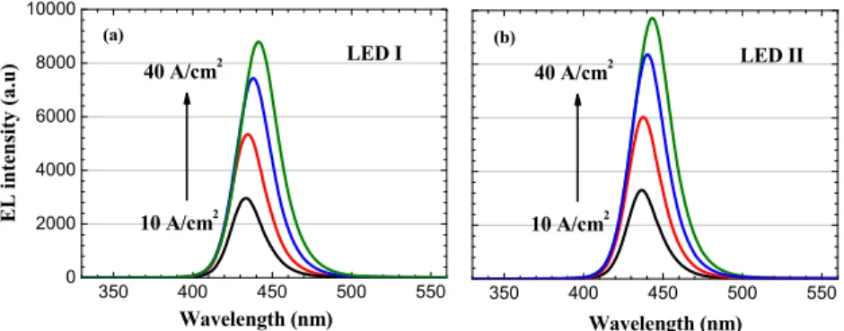
The measured EL spectra are shown in Figs. 1(a) and 1(b) for LEDs I and II, respectively. It can be seen that the EL intensity for LED II is stronger than that for LED I from lower injection current density of 10 A/cm2 to higher injection current density of 40 A/cm2. We also
observed a red shift of the emission wavelengths as a function of the increased injection current for both LED samples, and we attributed the red shift of the emission wavelength to the increased junction temperature during testing [3–5].
350 400 450 500 550 0 2000 4000 6000 8000 10000 LED I 40 A/cm2 E L inte nsity (a.u) Wavelength (nm) (a) 10 A/cm2 350 400 450 500 550 LED II Wavelength (nm) (b) 40 A/cm2 10 A/cm2
Fig. 1. EL spectra for (a) LED I and (b) LED II under various injection current levels of 10, 20, 30 and 40 A/cm2.
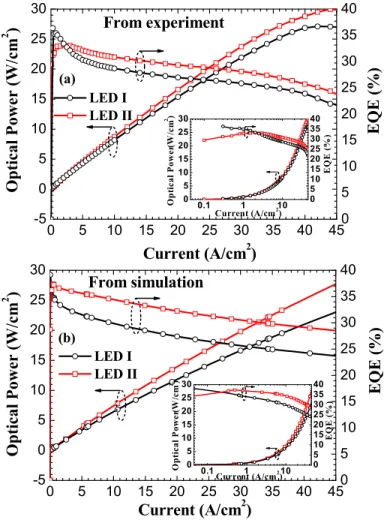
The experimentally measured integrated optical output power and the EQE are depicted in Fig. 2(a) for both LED samples. Being consistent with the EL spectra in Figs. 1(a) and 1(b), LED II emits stronger optical output power than LED I and the optical output power enhancement is 7.76% at 35 A/cm2 as an example. Correspondingly the EQE of LED II is
enhanced compared to that of LED I from low current density of 2 A/cm2 to high current
density of 45 A/cm2. More importantly, the efficiency droop
[droop=(EQE2 /A cm2 −EQEtest) /EQE2 /A cm2] for LED II is reduced significantly compared to LED I as shown in Fig. 2. For example, at 35 A/cm2, the droop is 24.01% and 18.03% for
LEDs I and II, respectively. The improved performance of LED II over LED I is attributed to the InGaN EC layer inserted before the InGaN/GaN MQW region. The detailed mechanisms of the InGaN EC layer on the improvement of the LED performance are theoretically investigated through the proposed mean-free-path model as follows. However, according to Fig. 2(a), both LEDs start the droop even when current density is smaller than 3 A/cm2, this is
likely due to the less optimized InGaN/GaN MQW region. In addition, the experimental efficiency of LED II is worse than that of LED I when the current density is lower than 2 A/cm2, which is due to the electron blocking effect by the InGaN EC layer when the electron
energy is small under the low bias. The simulated optical output power and EQE for LEDs I and II have also been illustrated in Fig. 2(b), and the simulated results are quite consistent with Fig. 2(a), in terms of the improved optical output power and reduced efficiency droop. However, the uncertainty of the III-nitrides such as the temperature dependence of the energy band offset, Auger recombination coefficient and Shockley-Read-Hall recombination coefficient causes the slightly different trending details between the simulated and measured optical properties.
0 5 10 15 20 25 30 35 40 45 -5 0 5 10 15 20 25 30 0.1 1 10 0 5 10 15 20 25 30 EQ E ( % ) O p ti ca l P ow er (W /c m 2) Current (A/cm2 ) 0 5 10 15 20 25 30 35 40 (a) From experiment EQ E ( % ) Op ti cal Power ( W /cm 2 ) Current (A/cm2) LED I LED II 0 5 10 15 20 25 30 35 40 0 5 10 15 20 25 30 35 40 45 -5 0 5 10 15 20 25 30 (b) From simulation LED I LED II EQ E ( % ) Optical Power (W/cm 2 ) Current (A/cm2) 0 5 10 15 20 25 30 35 40 0.1 1 10 0 5 10 15 20 25 30 EQ E ( % ) O p ti cal P ow er (W /c m 2) Current (A/cm2 ) 0 5 10 15 20 25 30 35 40
Fig. 2. (a) Experimentally measured and (b) numerically simulated optical output power and EQE for LEDs I and II, along with the optical output power and EQE in the semi-log scale in the insets.
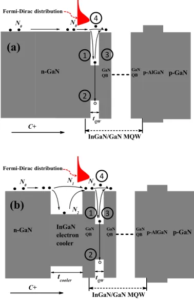
The schematic drawings of energy band diagrams of LED I and LED II are depicted in Figs. 3(a) and 3(b), respectively, along with four electron transport/transition processes in the InGaN/GaN MQWs. Note that the active region was grown directly after n-InGaN EC in the previous works [11–13]. Yet, the gained energy due to the conduction band offset between the n-GaN layer and n-InGaN EC (i.e., ΔEc) may accelerate the electrons again. Hence, in this work, we have purposely grown a 12 nm thick GaN barrier of 5 × 1017 cm−3 Si doping
concentration between the n-InGaN EC and the first quantum well. Then the gained ΔEccan be consumed by those electrons climbing over the next ΔEcbetween the n-InGaN EC and the adjacent GaN barrier. Moreover, our design is different from the one reported by Rebane et al. [17] In their design, they have grown a thin GaN barrier (0.5-5 nm) between the n-InGaN EC and the DH active region, hence transparent for electrons to tunnel through. However, as mentioned, the ΔEc between the n-GaN layer and the n-InGaN EC may accelerate the electrons again. On the other hand, we grow our LED samples along [0001] orientation, and thus we have to consider the acceleration effect on electrons through the polarization induced electric field within the n-InGaN EC, which is sandwiched between two GaN layers.
C+ InGaN electron cooler GaN N0 N0 n-GaN GaN QB GaN QB tQW p-AlGaN p-GaN InGaN/GaN MQW
(a)
1 2 3 4 n-GaN GaN QB tQW C+ tcooler N0 N0 N1 N2 InGaN electron cooler n-GaN GaN QB InGaN/GaN MQW p-AlGaN p-GaN GaN QB(b)
1 2 3 4 Fermi-Dirac distribution Fermi-Dirac distributionFig. 3. Schematic energy diagrams for (a) LED I and (b) LED II, along with which four electron transport/transition processes are depicted in the InGaN/GaN MQWs: electrons are captured into the quantum well, electrons recombine with holes and at defects, electrons re-escape from the quantum well and electrons directly fly over to a remote position without being captured by the quantum well.
According to Figs. 3(a) and 3(b), the incoming electrons are scattered and fall into the quantum wells (i.e., process ) with τcap being the electron capture time, and a value of 4 ×
10−12 s is used for electrons in the following simulations [18]. Those fallen electrons
thereafter on one hand are trapped onto the quantum energy levels and become bound electrons. Then, the recombination with holes and also in crystal defects takes place and it is depicted by process . The radiative recombination rates within the quantum wells can be generally expressed by Rrad =
(
n n− 0)
/τrad, where n is the electron concentration received by process while n0 is the thermal-equilibrium electron concentration and τrad is the radiativerecombination lifetime. Therefore, an increased n favors the radiative recombination processes. However, there is also a thermionic electron re-escape from the quantum wells and electrons become free again as illustrated by process in Figs. 3(a) and 3(b). The re-escape process is modeled by the electron escape time, i.e., τesc, and it can be expressed by
/
esc e tQW n Je
τ = ⋅ ⋅ [19], where n presents the electron concentration received by process
while Je is the electron current caused by thermionic emission in any heterojunction. Process
denotes those electrons of a longer mean free path traveling to a remote position without being captured by quantum wells, which has to be suppressed for an enhanced n.
Now we have to find an approach to increase the electron concentration in the quantum wells. We set the number of the electrons injected into the n-GaN region to N0 for both LED
samples. We neglect the electron loss through Shockley-Read-Hall (SRH) recombination in the n-GaN and n-In0.10Ga0.90N EC layers to simplify our model since the crystal quality of the
two samples is identical. Furthermore, the hole concentration in the n-In0.10Ga0.90N EC is
much lower than the electron concentration, so the electron loss through radiative recombination with holes is also negligible. For LED II with n-In0.10Ga0.90N EC layer, we
assumed electrons of N2 are captured by the n-In0.10Ga0.90N EC layer with LO phonon
emission, while the remaining electrons of N1 directly fly over the EC layer without
undergoing thermalization. The electrons of N2 are then injected into InGaN/GaN MQW
region after undergoing thermalization. Here, we correlate the quantum well captured electrons [i.e., process in Figs. 3(a) and 3(b)] with the electron mean free path (MFP) by Eq. (1) and Eq. (2) for LEDs I and II, respectively [20]. Note that the electron loss due to processes and contribute to the electron overflow from the MQW region.
(
)
0 1 exp( / ) 1 2 1 exp( / )
t QW MFP QW MFP
N =N × − −t l = N +N × − −t l (1)
1 1 exp( / ) 2 1 exp( / cooler)
t QW MFP QW MFP
M =N × − −t l +N × − −t l (2)
where tQWis the thickness of the quantum well, lMFP is the mean free path of electrons within the InGaN/GaN MQWs without electron thermalization and cooler
MFP
l is the mean free path of electrons in the InGaN/GaN MQWs with electron thermalization in the n-In0.10Ga0.90N EC
layer. Here, the relationship between N0 and N2 in Fig. 3(b) can be expressed in Eq. (3), in
which we assume the mean free path of electrons in the GaN layer before entering the n-In0.10Ga0.90N EC layer is lMFP. It is shown that, in order to have more electrons thermalized, it is useful to properly increase the thickness of the n-In0.10Ga0.90N EC layer (tcooler).
[
]
2 0 1 exp( cooler/ MFP)
N =N × − −t l (3)
The comparison between Eqs. (1) and (2) reveals that, to increase the number of the quantum well captured electrons, the electron mean free path within the InGaN/GaN MQW region must be reduced such that cooler
MFP MFP
l <l . Therefore, one has to understand the working mechanisms of the InGaN EC layer in reducing the electron mean free path. The electron mean free path is a function of the thermal velocity (i.e., vth- electron thermal velocity before undergoing thermalization and cooler
th
v - electron thermal velocity after undergoing thermalization) and the scattering time (τSC), which is set to 0.0091ps [11,12], as shown in Eqs. (4.1) and (4.2), respectively. Moreover, vth and cooler
th
v can be expressed in Eqs. (5.1) and (5.2), respectively. MFP th SC l =v ×τ (4.1) cooler cooler MFP th SC l =v ×τ (4.2) 2 [ ] / th e v = × +E qV m (5.1)
2 [ ] / 2 [ ] / cooler th c LO c e LO e v E E qV E m E qV m ω ω = × + Δ − + − Δ = × + − (5.2)
where E is the excess kinetic energy in the n-GaN layer referenced to the conduction band of the n-GaN layer, and me is the effective mass of electrons. The first ΔEcrepresents the kinetic energy received by the electrons when jumping over the conduction band offset between n-GaN and n-In0.10Ga0.90N EC layer. −ωLO means the energy loss by phonon emission. qVis the work done to the electrons by the polarization induced electric field in the in-plane compressive n-In0.10Ga0.90N EC layer. The −ΔEcin Eq. (5.2) depicts the energy loss for electrons when climbing over the conduction band offset between the n-In0.10Ga0.90N EC
layer and the first quantum barrier. In our calculation, in order to consider the crystal relaxation by generating misfit dislocations, we only assumed 40% of the theoretical polarization induced charge density [21]. Meanwhile, we assume the energy band offset ratio between InGaN and GaN to be 70:30 [22], and thus ΔEcbetween n-GaN and n-In0.10Ga0.90N
EC layer is 379.64 meV. Here we also assume the thermionic emission process dominates over the intra-band tunneling in the process of the electrons transport into the first quantum well. Thus ΔEccan be eliminated as shown in Eq. (5.2). The energy loss through LO phonon emission is 92 meV, i.e., ωLO = 92 meV [23]. Since the electric field within the EC layer is not linear and varies with position, we use APSYS simulator to calculate it [3]. The calculated electric field is shown in Fig. 4. Since
0
( )
cooler
t
qV =
q E y dy× , qV equals to 27.82 meV in our case. When the carrier temperature is 500 K, lMFP is 14.47 nm while coolerMFP
l is 1.32 nm. Obviously the In0.10Ga0.90N EC layer has a significant effect in reducing the electron mean
free path in InGaN/GaN MQWs, and therefore increasing the quantum well capture efficiency of electrons, i.e., Mt >Nt. Here we only consider the constant mean free path in InGaN/GaN MQWs and did not consider its position dependence since doing so will not change the conclusion but only add more complexity to the calculation. Note, the electrons follow Fermi-Dirac distribution, and therefore Eq. (5.2) is valid when E qV+ −ωLO >0 for those hot electrons with a high carrier temperature, while for those with E qV+ −ωLO <0 (i.e.,
c LO c
E+ Δ −E ω +qV < ΔE ) will be blocked by the conduction band offset between the EC layer and the first quantum barrier. However, the electrons will be accumulated in the EC layer until a high electron density is obtained, thus according to
(
)
2 * 3 4 ( ) exp / ln / B e e c B c e k T J m E k T n N h π ⋅ ⋅ ⋅= ⋅ −Δ + [24], where ΔEc is the conduction
band offset between GaN and the EC layer, andNcis the effective density of state for electrons, while kBis Boltzmann constant, m*eis the electron effective mass, h is the Planck constant and n is the electron density, the electrons still can transport into the active region.
0.000 0.005 0.010 0.015 0.020 -5x10⁵ -4x10⁵ -3x10⁵ -2x10⁵ -1x10⁵ 0 1x10⁵ 2x10⁵ 3x10⁵ 4x10⁵
El
ectr
ic Fi
eld
(V
/c
m)
Relative Position (
μm)
C+Fig. 4. Calculated electric filed as a function of position within the EC layer at 20 A/cm2. The positive direction of the electric field is along the growth orientation, i.e., C + .
With the above calculated values of the electron mean free path, we performed numerical simulations on the energy band diagrams, electron and hole distributions, electron currents and the radiative recombination rates for the two samples to confirm that the reduction of the electron mean free path by the In0.10Ga0.90N EC layer can enhance the optical output power
performance of LEDs. In our simulation, APSYS simulator is used, which can well model the carrier transport processes [i.e., processes , , , and in Figs. 3(a) and 3(b)] within the InGaN/GaN MQW region. The model of electron tunneling through the GaN layer between the n-InGaN EC and the first quantum well has not been used purposely to study the thermionic process for electron transport within that region. Besides the previously mentioned band offset ratio and polarization charge level, we also assumed 1 × 10⁻³⁰ cm6/s as the Auger
recombination coefficient [25]. The SRH recombination lifetime in the InGaN/GaN MQW region is set to be 43 ns [25]. Other parameters for nitrogen-containing compounds used in the simulation can be found somewhere else [26].
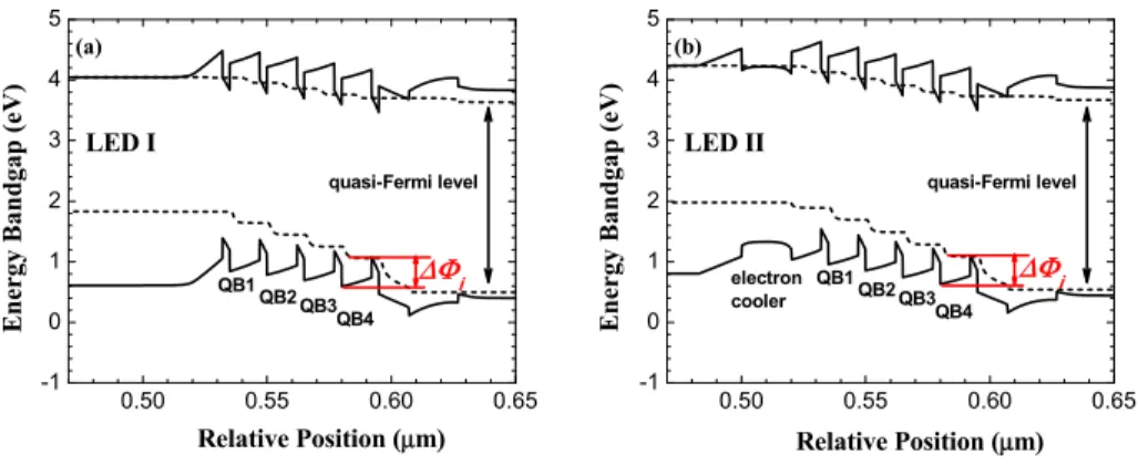
0.50 0.55 0.60 0.65 -1 0 1 2 3 4 5 LED I (a) QB4 QB3 QB2 E n ergy Ba ndg ap (eV ) Relative Position (μm) QB1 ΔΦi quasi-Fermi level 0.50 0.55 0.60 0.65 -1 0 1 2 3 4 5 LED II quasi-Fermi level electron cooler (b) E n ergy Ba ndg ap (eV ) Relative Position (μm) QB4 QB3 QB2 QB1 ΔΦi
Fig. 5. Energy band diagrams for (a) LED I and (b) LED II.
The simulated energy band diagrams at 20 A/cm2 for LEDs I and II are shown in Figs.
different quantum barriers (QB1, QB2, QB3 and QB4). The value of ΔΦiare extracted and demonstrated in Table 1, from which we can see the effective valence band barrier heights of the quantum barriers for LED II is smaller than those for LED I. It has been reported that the effective valance band barrier height for the p-EBL can be reduced by employing GaN/InGaN as the last quantum barrier, hence promoting the hole injection into InGaN/GaN MQWs [27, 28]. However, as found in this work, the same physical principle can be applied to the case when the n-type In0.10Ga0.90N layer is inserted between n-GaN layer and InGaN/GaN MQW
region. As the polarization induced electric field within the n-type In0.10Ga0.90N layer opposes
the built-in electric field of the diode, and thus the n-type In0.10Ga0.90N layer “pulls up” the
valance band of the MQWs for a better hole transport across the active region.
Table 1. Effective Valence Band Barrier Heights of InGaN/GaN MQWs for LEDs I and II
ΔΦ1 ΔΦ2 ΔΦ3 ΔΦ4
LED I 792.98 meV 666.84 meV 553.80 meV 489.90 meV
LED II 742.00 meV 638.99 meV 532.50 meV 447.29 meV
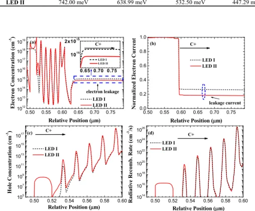
0.50 0.55 0.60 0.65 0.70 0.75 1012 1013 1014 1015 1016 1017 1018 1019 0.65 0.70 0.75 1015 2x10¹⁵ LED I LED II electron leakage (a) El ectr on Co ncen tra ti on (cm -3 ) Relative Position (μm) LED I LED II C+ 0.50 0.55 0.60 0.65 0.70 0.75 0.0 0.2 0.4 0.6 0.8 1.0 leakage current (b) No rma li zed El ect ro n C urre nt LED I LED II Relative Position (μm) C+ 0.50 0.52 0.54 0.56 0.58 0.60 105 107 109 1011 1013 1015 1017 (c) Relative Position (μm) Hole Co nc en tr at ion (c m -3 ) LED I LED II C+ 0.50 0.52 0.54 0.56 0.58 0.60 1014 1016 1018 1020 1022 1024 1026 (d) LED I LED II Ra di ativ e R eco mb. Ra te (c m -3 /s) Relative Position (μm) C+
Fig. 6. Simulated (a) electron concentration along with the inset depicting the electron leakage out of the active region, (b) normalized electron current, (c) hole concentration, and (d) radiative recombination rates at 20 A/cm2 across the InGaN/GaN MQW region for LEDs I and II, respectively.
The simulated electron profiles for LEDs I and II are shown in Fig. 6(a). We can see that the electron overflow is reduced in LED II with the n-type In0.10Ga0.90N EC layer, compared
to that in LED I. Meanwhile, the electron current distribution is also depicted in Fig. 6(b). Being consistent with Fig. 6(a), the electron leakage current into the p-type region is reduced from 26.56% to 18.86% at 20 A/cm2, if we compare LED II to LED I. It should be
noteworthy that the thermionic emission for process in Figs. 3(a) and 3(b) can also be
expressed by
(
)
2 * _ 3 4 ( ) exp / ln / B e e c wb B c e k T J m E k T n N h π ⋅ ⋅ ⋅ = ⋅ −Δ + [24], where ΔEc wb_ isthe conduction band offset for InGaN/GaN MQWs, andNcis the effective density of state for electrons, while kBis Boltzmann constant, m*eis the electron effective mass and h is the Planck constant. We can conclude that an increased electron concentration (i.e., n) within the InGaN/GaN MQWs enhances the electron re-escape process in Figs. 3(a) and 3(b) [29]. However, we know that Mt >Nt , and thus LED II has a more severe electron re-escape process than LED I in Figs. 3(a) and 3(b). As a result, the reduced electron leakage in LED II is well attributed to the reduced electron mean free path by the n-type In0.10Ga0.90N EC layer
that suppresses those electrons directly flying over the quantum wells. In addition, we also showed the hole profiles for LEDs I and II in Fig. 6(c), respectively. According to Fig. 6(c), we can see that LED II exhibits a more homogenous hole distribution across the InGaN/GaN MQWs than LED I, which is due to the reduced valence band barrier heights of InGaN/GaN MQWs by the InGaN EC layer as shown in Fig. 5. The radiative recombination rates for LEDs I and II are shown in Fig. 6(d). The increased electron capture efficiency and the improved hole transport in the InGaN/GaN MQWs due to the InGaN EC layer account for the enhanced radiative recombination rate for LED II, as indicated in Fig. 6(d).
4. Conclusions
In conclusion, the InGaN/GaN LED with an n-type In0.10Ga0.90N electron cooler layer has
been demonstrated and investigated. The enhanced electron capture efficiency by the multiple quantum wells is attributed to a reduced mean free path after electrons undergo thermalization by phonon emission in the electron cooler layer. Moreover, we found the n-type In0.10Ga0.90N
electron cooler layer also promotes the hole transport by “pulling up” the valence band of the quantum barriers. Thus, the increased electron capture efficiency and the improved hole transport across the multiple quantum wells lead to the improvement of the radiative recombination rate, and thus the enhanced optical output power and the reduced efficiency droop. Therefore, the InGaN electron cooler holds great promise for achieving better-performance InGaN/GaN LEDs and can be optimized using the electron mean-free-path model.
Acknowledgments
This work is supported by the National Research Foundation of Singapore under Grant No. NRF-CRP-6-2010-2 and NRF-RF-2009-09 and the Singapore Agency for Science, Technology and Research (A*STAR) SERC under Grant No. 112 120 2009.