Solar-blind AlGaN-based Schottky photodiodes with low noise and high detectivity
Necmi Biyikli, Orhan Aytur, Ibrahim Kimukin, Turgut Tut, and Ekmel Ozbay
Citation: Appl. Phys. Lett. 81, 3272 (2002); doi: 10.1063/1.1516856 View online: http://dx.doi.org/10.1063/1.1516856
View Table of Contents: http://aip.scitation.org/toc/apl/81/17
Published by the American Institute of Physics
Articles you may be interested in
Solar-blind AlGaN photodiodes with very low cutoff wavelength
Applied Physics Letters 76, 403 (2000); 10.1063/1.125768
High quantum efficiency AlGaN solar-blind p-i-n photodiodes
Applied Physics Letters 84, 1248 (2004); 10.1063/1.1650550
Improved solar-blind detectivity using an heterojunction photodiode
Applied Physics Letters 80, 3754 (2002); 10.1063/1.1480484
Gain mechanism in GaN Schottky ultraviolet detectors
Applied Physics Letters 79, 1417 (2001); 10.1063/1.1394717
Solar-blind AlGaN-based inverted heterostructure photodiodes
Applied Physics Letters 77, 316 (2000); 10.1063/1.126962
Role of self-trapped holes in the photoconductive gain of β-gallium oxide Schottky diodes
Solar-blind AlGaN-based Schottky photodiodes with low noise
and high detectivity
Necmi Biyiklia)and Orhan Aytur
Department of Electrical and Electronics Engineering, Bilkent University, Bilkent Ankara 06533, Turkey Ibrahim Kimukin, Turgut Tut, and Ekmel Ozbay
Department of Physics, Bilkent University, Bilkent Ankara 06533, Turkey 共Received 11 July 2002; accepted 27 August 2002兲
We report on the design, fabrication, and characterization of solar-blind Schottky photodiodes with low noise and high detectivity. The devices were fabricated on n⫺/n⫹ AlGaN/GaN heterostructures using a microwave compatible fabrication process. True solar-blind operation with a cutoff wavelength of ⬃274 nm was achieved with AlxGa1⫺xN (x⫽0.38) absorption layer. The
solar-blind detectors exhibited⬍1.8 nA/cm2dark current density in the 0–25 V reverse bias regime, and a maximum quantum efficiency of 42% around 267 nm. The photovoltaic detectivity of the devices were in excess of 2.6⫻1012cm Hz1/2/W, and the detector noise was 1/f limited with a noise power density less than 3⫻10⫺29A2/Hz at 10 kHz. © 2002 American Institute of Physics. 关DOI: 10.1063/1.1516856兴
Photodetectors that operate only in the⬍280 nm spec-trum are named as solar-blind detectors due to their blind-ness to solar radiation within the atmosphere.1 Solar-blind photodetectors are essential components for a number of ap-plications including missile plume detection, flame/engine control, and chemical/biological agent sensing. AlxGa1⫺xN-based photodetectors potentially offer significant
advantages over the current photomultiplier tube and silicon-based solar-blind detector technology in terms of size, com-plexity, cost, robustness, stability, power demands, and bandwidth.2 Moreover, its intrinsic solar blindness 共for x ⭓0.38) and the ability of operation under harsh conditions 共high-temperature and high power levels兲 due to its wide band gap makes AlxGa1⫺xN-based photodetectors attractive
for high-performance solar-blind detection applications. Sev-eral research groups have demonstrated successful solar-blind operation with AlxGa1⫺xN photodetectors using photoconductive,3,4 p – i – n,5–14 metal–semiconductor– metal共MSM兲,15,16and Schottky17–20detector structures. Cut-off wavelengths (c) as short as ⬃225 nm, an ultraviolet/
visible rejection over 5 orders of magnitude along with responsivities as high as 0.12 A/W at 232 nm were reported using a Al0.7Ga0.3N p – i – n detector structure.6,11Al0.5Ga0.5N
MSM photodiodes with a noise equivalent power 共NEP兲 as low as 30 fW at 280 nm and detectivity of 2.5 ⫻1013cm Hz1/2/W correspond to the best noise performance
achieved for AlGaN-based solar-blind detectors.15 Dark cur-rents less than 2 pA at 30 V reverse bias and a 3 dB band-width of 100 MHz was reported for a Al0.4Ga0.6N MSM
structure.16 Al0.35Ga0.65N p – i – n photodiodes on SiC
sub-strates with low leakage currents were also successfully demonstrated.12
When compared with p – i – n photodiodes, AlGaN Schottky photodiodes have several advantages. Growth of p-type doped AlGaN layers and formation of low resistance
p⫹ ohmic contacts are two challenging issues for p – i – n photodiodes, while Schottky photodiodes do not face these problems. Besides the ease of growth and fabrication, effi-cient collection of generated carriers within the junction and better high-frequency characteristics are the other advantages of AlGaN Schottky photodiodes. However, they lack from low efficiency mainly due to the optical absorption intro-duced by the thin Schottky metal, and exhibit high leakage currents and poor noise performance. The reported best de-tector performances obtained with solar-blind AlGaN Schottky photodiodes include a maximum responsivity of 0.07 A/W at 290 nm along with a NEP of 6.6⫻10⫺9 W,18a minimumcof 278 nm and a minimum dark current density
of 6.6⫻10⫺6A/cm2.19 In this letter, we demonstrate low noise solar-blind AlGaN-based Schottky photodiodes with very low dark current and high detectivity.
The epitaxial structure of the front-illuminated Schottky detector wafer was designed to achieve true solar-blindness, low leakage, and high solar rejection. In order to meet these requirements, Al0.38Ga0.62N absorption layer was used to
achieve c⬍280 nm. The AlxGa1⫺xN/GaN epitaxial layers
of our heterojunction Schottky photodiode wafer were grown on a 2 in. single-side polished共0001兲 sapphire substrate us-ing metalorganic chemical vapor deposition. A thin AlN nucleation layer was first deposited followed by a 0.5 m thick unintentionally doped GaN mesa isolation layer. After-ward, a highly doped (n⫹⫽2⫻1018cm⫺3) ohmic contact layer composed of 0.6 m thick GaN and 0.2 m thick Al0.38Ga0.62N were grown, respectively. The growth of the Schottky heterostructure was completed with the deposition of a 0.8 m thick undoped Al0.38Ga0.62N active layer. The highly doped GaN layer was used for ohmic contact region due to the difficulty of obtaining high-quality ohmic contacts with AlxGa1⫺xN layers. The n-type doped 0.2 m thick
Al0.38Ga0.62N layer was used as a diffusion barrier for the
photocarriers generated in the GaN ohmic contact layer. Such a diffusion barrier is expected to increase the solar-blind/near-UV rejection ratio of the detector.
a兲Electronic mail: [email protected]
APPLIED PHYSICS LETTERS VOLUME 81, NUMBER 17 21 OCTOBER 2002
3272
The samples were fabricated by using a four-step microwave-compatible fabrication process in a class-100 clean room environment. First, the ohmic contact regions were defined via reactive ion etching 共RIE兲 under CCl2F2 plasma, 20 sccm gas flow rate, and 100 W rf power. The etch rates for GaN and Al0.38Ga0.62N layers were determined as 300 and 80 Å/min, respectively. After an ohmic etch of⬃1.3 m, Ti/Al共100 Å /1000 Å兲 contacts were deposited via ther-mal evaporation and left in acetone solution for lift-off pro-cess. The contacts were annealed at 700 °C for 30 s in a rapid thermal annealing system. Mesa structures of the de-vices were formed via the same RIE process, by etching all the layers (⬎1.6m) down to the undoped GaN mesa iso-lation layer. Then, a ⬃100 Å thick Au film was evaporated to form the Au/AlGaN Schottky contacts. Finally, a ⬃0.7m thick Ti/Au interconnect metal was deposited and lifted off to connect the Schottky layers to coplanar wave-guide transmission line pads.
The resulting AlGaN Schottky photodiodes had break-down voltages above 50 V and turn-on voltages around 2 V. Figure 1 shows the current–voltage (I – V) characteristics of a 150⫻150m2 device. The leakage current of the diodes was lower than 1 pA for reverse bias voltages up to 30 V. As can be observed in the logarithmic plot, the dark current fluctuated within 150– 400 fA in the 0–25 V reverse bias range. The actual leakage values in this range could not be measured due to the measurement setup resolution. These leakage values correspond to dark current density values of 0.7– 1.8 nA/cm2. Hence, we can safely claim that our
solar-blind detectors exhibited dark current densities lower than 1.8 nA/cm2under reverse bias voltages as high as 25 V. The
differential resistance (R⫽dV/dI) of our detectors was cal-culated and a dark impedance in excess of 1013⍀ was ob-tained in the 0–25 V range.
Spectral photoresponse measurements were done in the 250–350 nm range, using a xenon lamp light source, a single-pass monochromator, a lock-in amplifier, and a cali-brated Si photodetector. Figure 2共a兲 shows the measured spectral quantum efficiency under reverse bias voltages rang-ing from 0 to 50 V. The quantum efficiency increased with reverse bias and reached a maximum value of⬃42% at 267
nm under 50 V reverse bias. The cutoff wavelength red-shifted with reverse bias, from 266 to 274 nm for 0 and 50 V reverse bias, respectively. Since c⬍280 nm was satisfied,
true solar-blind detection was successfully demonstrated. The corresponding device responsivity curve under 50 V re-verse bias is shown in Fig. 2共b兲. A peak responsivity of 0.09 A/W at 267 nm is measured. The responsivity drops sharply around 270 nm and a solar-blind/near-UV contrast of 4 or-ders of magnitude is observed within 80 nm. To estimate the detectivity (D*) of our detectors in the photovoltaic mode, we have used the thermal-noise limited detectivity relation D*⫽R(R0A/4kT), where R is the device reponsivity at
zero bias, R0 is the zero volt dark impedance and A is the
detector area. With a 0.01 A/W photovoltaic responsivity at 250 nm, the zero-bias detectivity of our detectors were in excess of 2.6⫻1012 cm Hz1/2/W, which corresponds to a setup limited NEP of 5.8⫻10⫺15W/Hz1/2.
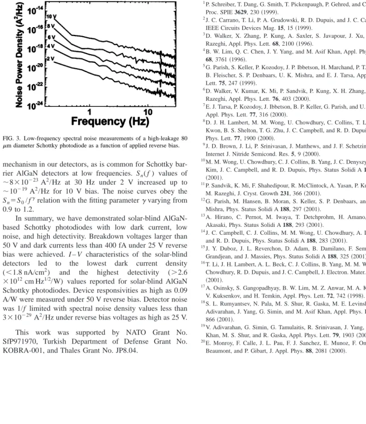
Finally, noise characterization of the solar-blind Schottky detectors were carried out in the frequency range of 1 Hz–100 kHz using a fast Fourier transform spectrum ana-lyzer and a microwave probe station. Our low-leakage, high-breakdown voltage solar-blind detectors had noise power densities below the instrument resolution. Even under re-verse bias as high as 25 V, the detector noise did not exceed the measurement setup noise floor of 3⫻10⫺29A2/Hz around 10 kHz. Therefore, we have measured devices with higher leakage currents in order to observe the bias depen-dence of the spectral noise density. Figure 3 shows the low-frequency spectral noise density of a 80m diameter detec-tor with ⬃7 orders of magnitude larger dark currents (⬎1A@5 V) and⬃14 V breakdown voltage. The spectral noise curves show that 1/f noise is the dominant noise FIG. 1. (I – V) characteristics of a 150⫻150m2solar-blind Schottky
pho-todiode. Inset shows the same data plotted in logarithmic scale.
FIG. 2. 共a兲 Measured spectral quantum efficiency of the AlGaN Schottky photodiode.共b兲 Corresponding responsivity curve of the device under 50 V reverse bias.
3273 Appl. Phys. Lett., Vol. 81, No. 17, 21 October 2002 Biyikliet al.
mechanism in our detectors, as is common for Schottky bar-rier AlGaN detectors at low frequencies. Sn( f ) values of
⬃8⫻10⫺23A2/Hz at 30 Hz under 2 V increased up to
⬃10⫺19A2/Hz for 10 V bias. The noise curves obey the
Sn⫽S0/ f␥relation with the fitting parameter␥varying from 0.9 to 1.2.
In summary, we have demonstrated solar-blind AlGaN-based Schottky photodiodes with low dark current, low noise, and high detectivity. Breakdown voltages larger than 50 V and dark currents less than 400 fA under 25 V reverse bias were achieved. I – V characteristics of the solar-blind detectors led to the lowest dark current density (⬍1.8 nA/cm2) and the highest detectivity (⬎2.6 ⫻1012cm Hz1/2/W) values reported for solar-blind AlGaN
Schottky photodiodes. Device responsivities as high as 0.09 A/W were measured under 50 V reverse bias. Detector noise was 1/f limited with spectral noise density values less than 3⫻10⫺29A2/Hz under reverse bias voltages as high as 25 V. This work was supported by NATO Grant No. SfP971970, Turkish Department of Defense Grant No. KOBRA-001, and Thales Grant No. JP8.04.
1P. Schreiber, T. Dang, G. Smith, T. Pickenpaugh, P. Gehred, and C. Litton, Proc. SPIE 3629, 230共1999兲.
2J. C. Carrano, T. Li, P. A. Grudowski, R. D. Dupuis, and J. C. Campbell, IEEE Circuits Devices Mag. 15, 15共1999兲.
3
D. Walker, X. Zhang, P. Kung, A. Saxler, S. Javapour, J. Xu, and M. Razeghi, Appl. Phys. Lett. 68, 2100共1996兲.
4B. W. Lim, Q. C. Chen, J. Y. Yang, and M. Asif Khan, Appl. Phys. Lett.
68, 3761共1996兲.
5
G. Parish, S. Keller, P. Kozodoy, J. P. Ibbetson, H. Marchand, P. T. Fini, S. B. Fleischer, S. P. Denbaars, U. K. Mishra, and E. J. Tarsa, Appl. Phys. Lett. 75, 247共1999兲.
6
D. Walker, V. Kumar, K. Mi, P. Sandvik, P. Kung, X. H. Zhang, and M. Razeghi, Appl. Phys. Lett. 76, 403共2000兲.
7E. J. Tarsa, P. Kozodoy, J. Ibbetson, B. P. Keller, G. Parish, and U. Mishra, Appl. Phys. Lett. 77, 316共2000兲.
8
D. J. H. Lambert, M. M. Wong, U. Chowdhury, C. Collins, T. Li, H. K. Kwon, B. S. Shelton, T. G. Zhu, J. C. Campbell, and R. D. Dupuis, Appl. Phys. Lett. 77, 1900共2000兲.
9
J. D. Brown, J. Li, P. Srinivasan, J. Matthews, and J. F. Schetzina, MRS Internet J. Nitride Semicond. Res. 5, 9共2000兲.
10M. M. Wong, U. Chowdhury, C. J. Collins, B. Yang, J. C. Denyszyn, K. S. Kim, J. C. Campbell, and R. D. Dupuis, Phys. Status Solidi A 188, 333
共2001兲.
11P. Sandvik, K. Mi, F. Shahedipour, R. McClintock, A. Yasan, P. Kung, and M. Razeghi, J. Cryst. Growth 231, 366共2001兲.
12
G. Parish, M. Hansen, B. Moran, S. Keller, S. P. Denbaars, and U. K. Mishra, Phys. Status Solidi A 188, 297共2001兲.
13A. Hirano, C. Pernot, M. Iwaya, T. Detchprohm, H. Amano, and I. Akasaki, Phys. Status Solidi A 188, 293共2001兲.
14J. C. Campbell, C. J. Collins, M. M. Wong, U. Chowdhury, A. L. Beck, and R. D. Dupuis, Phys. Status Solidi A 188, 283共2001兲.
15J. Y. Duboz, J. L. Reverchon, D. Adam, B. Damilano, F. Semond, N. Grandjean, and J. Massies, Phys. Status Solidi A 188, 325共2001兲. 16T. Li, J. H. Lambert, A. L. Beck, C. J. Collins, B. Yang, M. M. Wong, U.
Chowdhury, R. D. Dupuis, and J. C. Campbell, J. Electron. Mater. 30, 872
共2001兲.
17A. Osinsky, S. Gangopadhyay, B. W. Lim, M. Z. Anwar, M. A. Khan, D. V. Kuksenkov, and H. Temkin, Appl. Phys. Lett. 72, 742共1998兲. 18
S. L. Rumyantsev, N. Pala, M. S. Shur, R. Gaska, M. E. Levinshtein, V. Adivarahan, J. Yang, G. Simin, and M. Asif Khan, Appl. Phys. Lett. 79, 866共2001兲.
19V. Adivarahan, G. Simin, G. Tamulaitis, R. Srinivasan, J. Yang, M. Asif Khan, M. S. Shur, and R. Gaska, Appl. Phys. Lett. 79, 1903共2001兲. 20E. Monroy, F. Calle, J. L. Pau, F. J. Sanchez, E. Munoz, F. Omnes, B.
Beaumont, and P. Gibart, J. Appl. Phys. 88, 2081共2000兲.
FIG. 3. Low-frequency spectral noise measurements of a high-leakage 80 m diameter Schottky photodiode as a function of applied reverse bias.