PROCEEDINGS OF SPIE
SPIEDigitalLibrary.org/conference-proceedings-of-spieLow dark current N structure
superlattice MWIR photodetectors
Omer Salihoglu
Abdullah Muti
Rasit Turan
Yuksel Ergun
Atilla Aydinli
Low dark current N structure superlattice MWIR photodetectors
Omer Salihoglu
a,*, Abdullah Muti
b, Rasit Turan
c, Yuksel Ergun
dand Atilla aydinli
b aTUBITAK MAM, Energy Institute, Kocaeli, Turkey.
b
Bilkent University, Dept. of Physics, Ankara, Turkey.
c
Middle East Technical University, Dept. of Physics, Ankara, Turkey.
dAnadolu University, Dept. of Physics, Eskisehir, Turkey.
ABSTRACT
Commercially available read out integrated circuits (ROICs) require the FPA to have high dynamic resistance area product at zero bias (R0A) which is directly related to dark current of the detector. Dark current arises from bulk and
surface contributions. Recent band structure engineering studies significantly suppressed the bulk contribution of the type-II superlattice infrared photodetectors (N structure, M structure, W structure). In this letter, we will present improved dark current results for unipolar barrier complex supercell superlattice system which is called as “N structure”. The unique electronic band structure of the N structure increases electron-hole overlap under bias, significantly. N structure aims to improve absorption by manipulating electron and hole wavefunctions that are spatially separated in T2SLs, increasing the absorption while decreasing the dark current. In order to engineer the wavefunctions, we introduce a thin AlSb layer between InAs and GaSb layers in the growth direction which also acts as a unipolar electron barrier. Despite the difficulty of perfect lattice matching of InAs and AlSb, such a design is expected to reduce dark current. Experiments were carried out on Single pixel with mesa sizes of 100 × 100 – 700 × 700 µm photodiodes. Temperature dependent dark current with corresponding R0A resistance values are reported.
Keywords: Superlattice, Photodetector, InAs/GaSb, N design, barrier, SiO2, Passivation
1. INTRODUCTION
Search efforts to find alternatives for QWIP and mercury cadmium telluride (MCT) technologies have increased the attention on type II superlattice (T2SL) infrared photodetectors. T2SL has superior properties like band gap engineering [1], suppressed Auger recombination rates [2], reduced interband tunneling due to higher effective masses of electrons and holes [3]. These properties makes T2SL a very promising technology for most of the infrared region (3-30 µm). Furthermore T2SL becomes next key technology for military and medical applications. To achieve the state of art infrared photodetectors, further improvements such as, reducing the dark current level due to generation recombination (G-R) mechanisms and surface conductive channels, are needed. Especially low temperature requirement for the normal operation makes infrared detectors very unpractical for many applications. A detector working at hotter regime will reduce cost, volume and weight of the infrared imagining systems.
Placing a barrier inside the superlattice period is solved some of above problems by blocking one type of carriers and allowing other type of carriers. Famous material configurations such as, nBn design [4], PbIbN design [5], CBIRD structure [6] and M structure design [7] have been proposed and fabricated successfully. These designs easily and effectively reduced the dark current and increased the BLIP temperature over 100K. For example Nguyen et.al. proposed M structure to block thermal electrons to reduce dark current [7]. A AlSb layer has been placed inside the GaSb layer which enhances electron-hole wavefunctions overlap integral due to the AlSb barrier pushing the electron and hole wavefunctions towards the layer edges.
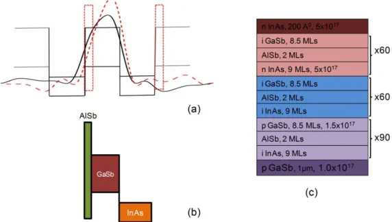
r--AISb (a) (b) i GaSb, 8.5 MLs AISb, 2 MLs n InAs, 9 MLs, 5x10¹⁷ i GaSb, 8.5 MLs AISb, 2 MLs i InAs, 9 MLs p GaSb, 8.5 MLs, 1.5x10¹⁷ AISb, 2 MLs i InAs, 9 MLs p GaSb,1 Nm, 1.0x10¹⁷ (c) x60 x60 x90
In this work, we fabricated square infrared photodetectors with using N design structure [8]. In this material design, an AlSb layer is placed between the InAs and GaSb layer in the growth direction. This design works similar to M design but it allows better electron-hole wavefunction overlap under reverse bias conditions, leading to efficient optical absorption. N design will give better optical performance and similar electrical performance when compared with the M design. However, due to relatively large constant mismatch between InAs (6.0584 Å) and AlSb (6.1355 Å) unlike AlSb on GaSb (6.0959 Å) unwanted trap states may be generated at the interface. This may be overcome with AlSb layers thinner than the critical thickness. Spitzer et. al showed that InSb like interfaces in AlSb/InAs superlattices grow perfectly pseudomorphically while AlAs like interfaces relax [9]. As will be shown, our dark current density measurements clarify that lattice mismatch does not reduce device performance.
2. EXPERIMENTAL
Conduction and valance band profiles for the proposed T2SL "N" structure is shown in figure 1a and 1b. Under bias, in a standard pin diode, electron and hole wavefunctions shift in opposite directions. Inserting an AlSb layer symmetrically into the middle of the GaSb layer leads to an increase of the overlap at the InAs/GaSb interface on the lower energy side of the AlSb barrier, while it becomes smaller at the InAs/GaSb interface on the higher energy side. However, when the AlSb barrier is introduced between GaSb and InAs layers, electron and hole wavefunctions are pushed away from the AlSb interface, increasing the overlap at the InAs/GaSb interface. Figure 1a shows the overlap integral with and without AlSb barrier under 0.001 meV bias per period. When there is no barrier (black line), overlap integral is shifted towards right side of the GaSb layer. With the AlSb barrier, (red line) the shift of the overlap integral towards the InAs/GaSb interface is enhanced. It is clear that barrier increases the overlap at the GaSb/InAs interface. Figure 1b shows a schematic of the N structure energy band diagram. Figure 1c shows layer makeup of the actual superlattice structure. It starts with 100 nm thick GaSb buffer layer and 20 nm Al(x)GaAs(y)Sb as an insulator and etch stop layer, followed by 1000 nm GaSb:Be (p=1.0x1017 cm -3) p contact layer.
P-i-n part of the design consist of 90 periods 9 monolayers (MLs) of InAs/2 MLs of AlSb/8.5 MLs of GaSb:Be (p=1.5x1017 cm-3) p-type layers, 60 periods 9 MLs of InAs/2 MLs of AlSb/8.5 MLs of GaSb i-layers, 40 periods 9
MLs of InAs:Te (n: 5x1017 cm -3)/ 2 MLs of AlSb/8.5 MLs of GaSb n-type layers and structure is terminated by 20
nm InAs:Te (n: 5x1017 cm -3) cap layer to assure good ohmic contact. The sample studied in this work was grown
commercially (IQE Inc. USA) with molecular beam epitaxy on a GaSb substrate.
Figure 1. (a) Overlap integral with (red line) and without (black line) AlSb barrier under 0.001 meV bias per period. (b) Schematic of the N structure energy band diagram. (c) Layer makeup of the actual superlattice structure.
2.5x1041
2.5x10³
---'
N 2
.5x 102
U
ci
Ca- 2.5x101
2.5x10°
_ i i2.5x10
500x500µm-1.0
i-0.5
,0.0
Bias(V)
i0.5
R120
R125 R130 R135 R140 R146 R150 R155 R159 R165 R170 R175 R180R185
R190 R195 R200 R205 R210 R215 R220 R225 R235 R2401.0
3. RESULTS AND DISCUSSIONS
Single pixel square photodetectors were fabricated with mesa sizes ranging from 100x100 to 700×700 µm2.
To minimize surface damage, mesas have been fabricated by standard lithography with phosphoric acid/citric acid based wet etch solution. The etch process has been stopped when etch depth reached the bottom contact layer. The complete fabrication processes can be found elsewhere [10]. A protective 250 nm thick SiO2 layer has been
deposited using plasma enhanced chemical vapor deposition (PECVD) system at 160 C0 with %2SiH
4/N2 and N2O
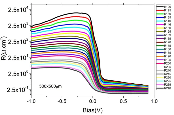
gas flows of 180 sccm and 225 sccm, respectively. Ohmic contacts were made by evaporating 5 nm Titanium (Ti) and 200 nm Gold (Au) on the bottom and top contact layers of the detectors. Sample was bonded to a 40 pin DIP chip carrier for further characterization. Electrical measurements of the “N” design superlattice barrier structure have been done by a HP4142OA source-measure unit. Samples were mounted on a He cooled closed cycle cold finger with a cold shield system. Dark current measurements were performed at temperatures between 30K and 250K. Figure 2 shows dynamic resistance measurement for 500 x 500 μm2 square single pixel photodetector at for
different temperatures. Even at 240K N design infrared photodetector shows a diode characteristic which is very promising towards the hot regime operation.
Figure 2. Dynamic resistance measurements for different temperatures.
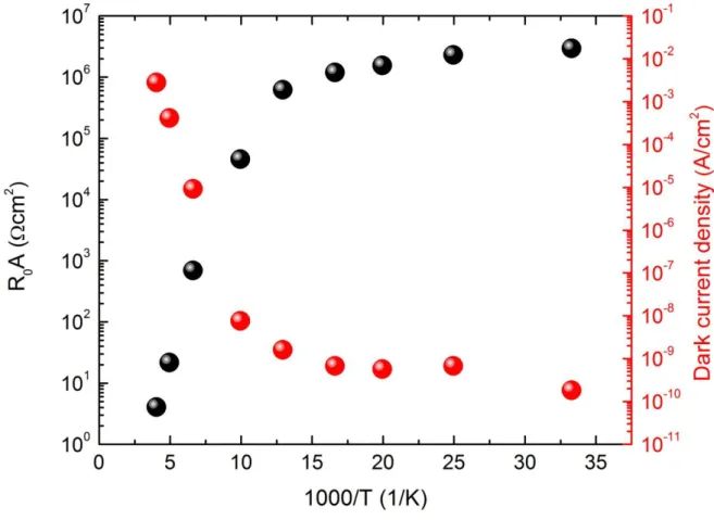
Figure 3shows dark current density and dynamic resistance area product vs. 1000/T graph for 700 x 700 µm2 photo-diode for different temperatures under zero bias. The I-V curve is dominated by diffusion current for
10'
106 105 104 103 102 101 100o
v
0
O
v
v
O
v
v
O
1O
,
CI o
a
O
5 10 1520
25
1000 /T (1 /K)
30
35
10 -' 10 -2 10-1° 10 -"higher temperatures, Arhenious type behavior has been observed. The activation energy has been determined as 0.281 eV which is very close to material bandgap. At 77K, dark current density and dynamic resistance at zero bias are measured as 1.5x10⁻⁹ A/cm2 and 6.1x10⁵ Ωcm2, respectively. This very low dark current density shows that
lattice mismatch of the InAs and AlSb does not cause a dramatic defective region at the interface. At 150K, dark current density and dynamic resistance at zero bias are measured as 1.5 x 10⁻⁶ A/cm2 and 6.8 x 10² Ωcm2,
respectively. These results are very promising for high temperature operation. This low dark current density satisfies the requirements of the commercially available read out integrated circuits (ROICs) for the operation at 150K.
Figure 3. Temperature dependent dark current density for type-II InAs/GaSb superlattice 700 x 700 µm2
photodiodes at zero bias voltage.
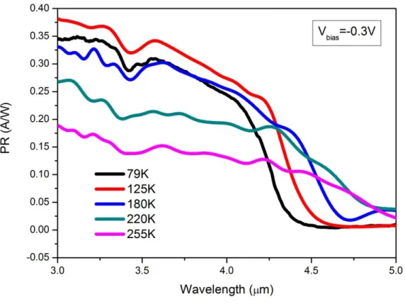
Spectral response of the photodetectors has been measured using calibrated blackbody source at 450 0C
(Newport, Oriel 67000), lock-in amplifier (SRS, SR830 DSP) and mechanical chopper (SRS, SR540) system. details of the measurement can be found elsewhere [11]. Quantum efficiency of the devices have been measured as %15 for single pass front illumination condition at wavelength of 3.5 µm. The quantum efficiency and absorbing region thickness are directly related to each other. Using thicker absorber layer will definitely increase the quantum efficiency of the photodetector. Figure 4 shows photo responsivity versus wavelength graph of the n structure photodetector for the operating temperatures between 79 K and 250 K. Under -0.3V bias, the peak D*, was determined as 2.9 x 10¹² Jones for the photodetectors at 4.0 µm and 77 K. BLIP temperature has been determined as
0.40 0.35 0.30 0.25 -30 3.5 4.0 Wavelength (pm) i 4.5 50
Figure 4. Photoresponsivity versus wavelength graph for the operating temperatures between 79 K and 250 K. Under -0.3V bias
IV. CONCLUSIONS
In conclusion, we fabricated photodetectors using N design structure with very low dark current and high dynamic resistance at 150K. At 150K, dark current density and dynamic resistance at zero bias are measured as 1.5 x 10⁻⁶ A/cm2 and 6.8 x 10² Ωcm2, respectively. These results are very promising for high temperature operation. This
low dark current density satisfies the requirements of the commercially available read out integrated circuits (ROICs) for the operation at 150K. At 77K, dark current density and dynamic resistance at zero bias are measured as 1.5x10⁻⁹ A/cm2 and 6.1x10⁵ Ωcm2, respectively. This very low dark current density shows that lattice mismatch of
the InAs and AlSb does not cause a dramatic defective region at the interface. Quantum efficiency (QE) of the photodetector has been determined as % 15 for single pass front illumination condition. Quantum efficiency can be further increased with thicker absorber regions and multipass designs. Temperature dependent dark current measurements revealed Arrhenius type of behavior with bulk diffusion current is effective for the temperatures higher than 120K. Since AlSb is only two monolayers thick, it does not seem to be generating large amount of electrically active interface states. Our results show that this lattice mismatch is not large enough to reduce device performance significantly. Photodetector reaches BLIP condition at 125K with the BLIP detectivity (D*
BLIP) of 2.6 x
REFERENCES
[1]. J. Wei and M. Razeghi, "Modeling of type-II InAs/GaSb superlattices using an empirical tight-binding method and interface engineering," Phys Rev B 69, 085316 (2004).
[2]. C. H. Grein, P. M. Young, and H. Ehrenreich, "Minority-Carrier Lifetimes in Ideal Ingasb/Inas Superlattices," Appl Phys Lett 61, 2905-2907 (1992).
[3]. D. L. Smith and C. Mailhiot, "Proposal for Strained Type-Ii Superlattice Infrared Detectors," J Appl Phys 62, 2545-2548 (1987).
[4]. J. B. Rodriguez, E. Plis, G. Bishop et al., "nBn structure based on InAs/GaSb type-II strained layer superlattices," Appl Phys Lett 91, 043514 (2007).
[5]. N. Gautam, H. S. Kim, M. N. Kutty et al., "Performance improvement of longwave infrared photodetector based on type-II InAs/GaSb superlattices using unipolar current blocking layers," Appl Phys Lett 96, 231107 (2010).
[6]. D. Z. Y. Ting, C. J. Hill, A. Soibel et al., "A high-performance long wavelength superlattice complementary barrier infrared detector," Appl Phys Lett 95 (2) (2009).
[7]. B. M. Nguyen, D. Hoffman, P. Y. Delaunay et al., "Dark current suppression in type II InAs/GaSb superlattice long wavelength infrared photodiodes with M-structure barrier" Appl. Phys. Lett. 91, 163511 (2007).
[8]. O. Salihoglu, A Muti, K Kutluer, T Tansel, R Turan, Y Ergun, A Aydinli, “N” structure for type-II superlattice photodetectors”, Applied Physics Letters 101 (7), 073505-073505-4, (2012). [9]. J. Spitzer, H. D. Fuchs, P. Etchegoin, M. Ilg, M. Cardona, B. Brar and H. Kroemer “Quality of
AlAs-like and InSb-like interfaces in InAs/AlSn superlattices: An optical study,” Appl. Phys. Lett. 62, 2274 (1993).
[10]. O. Salihoglu, A Muti, A Aydinli, “A Comparative Passivation Study for InAs/GaSb Pin Superlattice Photodetectors”, IEEE JOURNAL OF QUANTUM ELECTRONICS 49 , 661, (2013) [11]. O. Salihoglu, A. Muti, K. Kutluer et al., "Atomic Layer Deposited Al2O3 Passivation of