Investigation of high frequency performance limit of graphene field
effect transistors
Ercag Pince and Coskun Kocabasa兲
Department of Physics, Advanced Research Laboratories, Bilkent University, 06800 Ankara, Turkey 共Received 2 September 2010; accepted 6 October 2010; published online 26 October 2010兲 Extremely high field effect mobility together with the high surface coverage makes graphene a promising material for high frequency electronics application. We investigate the intrinsic high frequency performance limit of graphene field effect transistors limited by the charge impurity scattering. The output and transfer characteristics of graphene field effect transistors together with the high frequency performance are characterized as a function of impurity concentration and dielectric constant of the gate insulator. Our results reveal that graphene transistors could provide power gain at radio frequency band. © 2010 American Institute of Physics.
关doi:10.1063/1.3506506兴
Recent advances of chemical vapor deposition of graphene on large area substrates1–3 stimulate a significant research effort searching for new applications of graphene in the field of unusual electronics such as macroelectronics.4,5 Graphene can function as an effective semiconductor6,7or a transparent conducting coating1,8–10 for large area displays and photovoltatic devices. Recent developments in scaling of graphene films open up new opportunities for flexible electronics.1Extremely high field effect mobility of graphene together with the large area deposition process,2 could pro-vide alternative solutions for the challenges of traditional organic materials. Operation at radio frequencies is one of the main challenges of the organic based field effect transis-tors owing to the poor field effect mobilities of organic semi-conductors. Therefore radio frequency analog electronics could be an immediate high-end application of graphene transistors.11
Although high frequency analog electronics is a well es-tablished field for inorganic semiconducting materials, the effects of unusual transport properties of monoatomic graphene sheets at high frequencies are widely unknown. Recent experimental studies show several demonstrations of graphene and carbon nanotube arrays for high frequency operation.12–15 Cut-off frequencies of 10 GHz for carbon nanotube arrays14,16,17 and 100 GHz for graphene13,18 have been achieved. Using critical design considerations, these values can be advanced by orders of magnitude. There is little in the literature that provides a simple, yet quantitative model to analyze the critical design considerations of radio frequency operation of graphene based field effect transis-tors. This work is aiming to develop an analytical model to design a graphene based rf 共radio frequency兲 transistors based on diffusive transport governed by the charged impu-rity scattering.
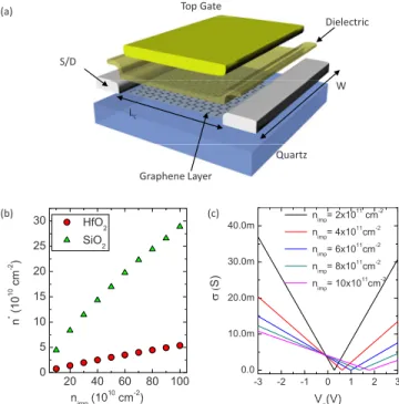
A schematic representation of a model rf transistor is shown in Fig. 1共a兲. The transistor consists of a graphene layer printed on an insulating substrate 共e.g., quartz or sap-phire兲. The source and drain electrodes are formed on the graphene layer. A thin layer of dielectric material functions as a gate dielectric for the field effect transistor
configura-tion. The gate electrode is formed on top of the gate dielec-tric. For the model, the dielectric thickness is 50 nm and the channel length and width are 1 m.
Here, we consider the transport mechanism governed by the charged impurity scattering owing to the presence of the charged impurities on the substrate and the gate dielectric. The dielectric constant of the surrounding medium 共gate di-electric and substrate兲 controls the effects of the impurity charges on the graphene layer. High-k dielectric materials 共e.g., HfO2兲 concentrate the electric field into the dielectric material and reduce the formation of residue charges on the graphene layer. Fang et al.19,20 confirmed the effect of the charge screening on the charge mobility of the graphene.20 Recent experimental results also agree with charge mobility lowering of graphene device by increasing charged
impuri-a兲Author to whom correspondence should be addressed. Electronic mail:
[email protected]. Tel.:⫹903122901965. Top Gate (a) S/D Dielectric W Lc Quartz Graphene Layer 30.0m 40.0m nimp= 2x10 11cm-2 nimp= 4x1011 cm-2 nimp= 6x1011cm-2 nimp= 8x10 11 cm-2 20 25 30 HfO2 SiO2 m -2 ) (c) (b) 10 0m 20.0m S) imp nimp= 10x1011cm-2 10 15 20 n * (10 10 cm -3 -2 -1 0 1 2 3 0.0 10.0m V (V) 20 40 60 80 100 0 5 n (1010 cm-2 ) Vg(V) nimp(10 cm )
FIG. 1. 共Color online兲 共a兲 Layout of a graphene based radio frequency transistor with a channel length Lcand channel width W.共b兲 The calculated residual charge concentration nⴱas a function of charged impurity concen-tration nimp for two different dielectric material HfO2 and SiO2.共c兲 The
conductivity of graphene layers as a function of gate voltage. The charged impurity concentration is scanned from 2⫻1011to 10⫻1011 cm−2. APPLIED PHYSICS LETTERS 97, 173106共2010兲
0003-6951/2010/97共17兲/173106/3/$30.00 97, 173106-1 © 2010 American Institute of Physics
ties with potassium doping.21For the top gate configuration, both substrate and the gate dielectric determine the effective dielectric constant. Therefore, the substrate should have high dielectric constant or has to be coated with high-k material, such as HfO2. A quartz wafer coated with a thin layer of HfO2, grown by atomic layer deposition, could be a good substrate for graphene based rf transistors.
In the present analysis of the radio frequency devices we consider a self-consistent transport model developed by Adam et al. based on a charged impurity scattering. This model explains the most of the observed electrical behavior of graphene sheets, e.g., nonuniversal minimum conductivity and ultrahigh mobility of suspended graphene layers. The beauty of the model is that it requires only a few empirical parameters, density of charged impurities and the distance between the impurity and graphene layer and the dielectric constant of the surrounding medium. The distance of charged impurities between graphene is effectively located around 0.1–1 nm from the graphene sheet.22
We have analyzed the frequency response of graphene devices in three steps. First, we have used the self consistent model23to calculate the residual charge concentration nⴱ on the graphene layer关Fig.1共b兲兴. After calculating the conduc-tivity from the residual charge concentration, then we calcu-lated the drain current at a given bias condition using a two-dimensional field effect transistor共FET兲 model. Scanning the gate and drain bias voltages we obtained the transfer and output curves of the device. Finally using the outcome of the device model we calculate the transconductance and associ-ated cut-off frequency of the devices.
The residual charge concentration on graphene layer nⴱ depends on the charge impurity concentration and the dielec-tric constant of the gate dielecdielec-tric and the substrate. Figure
1共b兲shows the graph of residual charge concentration nⴱas a function of charged impurity concentration nimpfor two dif-ferent dielectric material HfO2 and SiO2. SiO2 provides about six times more residue charges on graphene layer than HfO2owing to the low dielectric constant. Having calculated the residual charge concentration, we have calculated the conductivity of the graphene layer as a function of gate volt-age by Eq.共1兲.23 共n − n¯兲 =
冦
20e2nⴱ hnimp. if n − n¯⬍ nⴱ 20e2n hnimp. if n − n¯⬎ n ⴱ冧
, 共1兲where n¯ = nimp2 /4nⴱ. Here the carrier concentration n on the graphene layer is used as n = CoxVg, where Cox is the gate capacitance and Vgis the gate voltage. Figure1共c兲shows the calculated conductivity as a function of the gate voltage for impurity concentrations ranging from 2⫻1011 to 10 ⫻1011 cm−2.
For a bias point, the carrier density changes along the channel. Knowing the gate voltage dependence of the con-ductivity, the carrier density is calculated as a function of position along the channel. We have considered a constant contact resistance Rs of 1.2 k⍀ 共Ref. 24兲 between the source/drain electrodes and the graphene layer. For a two-dimensional FET model, the drain current is written as25
Id= W Lc
冕
0 Lc 共x兲E共x兲dx =W Lc冕
Vs−RsId Vd−RsId 共V兲dV, 共2兲where共x兲 is the conductivity and E共x兲 is the electric field along the graphene layer. With a change of variable including the voltage drops at the contacts, the integral becomes a simple transcendental equation. Solving this transcendental equation using the conductivity values calculated by Eq.共1兲 provides the drain current for a given biasing condition. Fig-ures 2共a兲and2共b兲 show transfer and output curves of a de-vice with a channel length of 1 m and channel width of 1 m. In this calculation we have used a 50 nm HfO2as a gate dielectric with a dielectric constant of 16. For these calculation, the only empirical parameter that we used is im-purity concentration on the dielectric and contact resistance between the electrodes and the graphene. This framework allows us to analyze the effect of the gate dielectric material on the device performance. Figure2共c兲shows the calculated transfer curves for different concentration of charge impuri-ties on the substrate. The Dirac point shifts to the higher voltages and the on/off ratio increases with increasing charge impurity concentration. The on/off ratio of the devices creases from 1.7 to 3.0 as the impurity concentration in-creases. Dependence of on/off ratio on the impurity concen-tration can be understood from the decreasing in minimum conductivity of the graphene layer as the impurity concentra-tion increases. This behavior provides a tradeoff between transconductance and output resistance for the high fre-quency performance.
High frequency performance limits can be understood by analyzing the cut-off frequency 共ft兲 of the device. Cut-off
600μ 0V 0.2V nimp=4x1011cm-2 600μ 1.0 V nimp=4x1011cm-2 (a) (b) 400μ Id (A) 0.4V 0.6V 0.8V 1V 1.2V 300μ 400μ 500μ 0.8 V 0.6 V Id (A) 200μ 100μ 200μ μ 0.4 V 0.2 V 0.0 0.5 1.0 0 Vd(V) 3.0 450μ 0 1 2 0 Vg(V) (c) (d) 0.7 0.8 2 4 2.6 2.8 x (mS) Hz) 300μ 350μ 400μ A ) 0.6 2.0 2.2 2.4 gm ma x ft (G H 150μ 200μ 250μ Id (A 2x1011 cm-2 4x1011 cm-2 6x1011 cm-2 8x1011 cm-2 2 4 6 8 10 0.5 1.8 nimp(1011cm-2) -2 -1 0 1 2 3 150μ Vg(V) 8x10 cm 10x1011 cm-2
FIG. 2. 共Color online兲 共a兲 The transfer curves for a graphene FET with a channel length of 1 m and channel width of 1 m. The gate dielectric used for the calculation is 50 nm HfO2. A clear ambipolar behavior and
current saturation because of contact resistance is seen on the transfer curves.共b兲 The output curves of the same device for the gate voltage range from 0 to 1.2 V. The curves in 共a兲 and 共b兲 are calculated for n=4 ⫻1011 cm−2.共c兲 The transfer curves for the device for different charged
impurity concentrations at a drain voltage of 0.6 V.共d兲 Calculated maximum transconductance of the device as a function of charged impurity concentration.
173106-2 E. Pince and C. Kocabas Appl. Phys. Lett. 97, 173106共2010兲
frequency is defined as the frequency where the current gain is 0 dB. After cut-off frequency the drain current due to the modulation of the channel conductivity is less than the gate leakage current. Gate capacitance and the small signal trans-conductance of a device determine the cut-off frequency as
ft= gm/2Cg. Figure 2共d兲 shows the calculated maximum transconductance of the device and the associated cut-off fre-quency as function of charged impurity concentration. The parallel plate gate capacitance is used for the calculation. Cleanest samples with charged impurity levels of 2⫻1011 have ftaround 25 GHz for 1 m channel length. The calcu-lated cut-off frequency decays down to 18 GHz as we in-crease the charged impurity concentration.
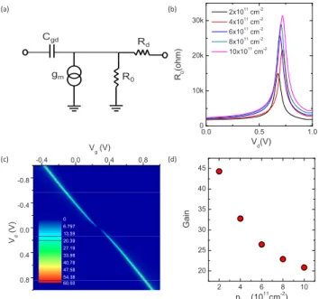
A small signal circuit model for the graphene devices is presented to understand the intrinsic high frequency perfor-mance. A simplified small-signal equivalent circuit model of a graphene device is given in Fig. 3共a兲. Cgd, gm, Rd, and R0 represent gate-drain capacitance, transconductance, drain re-sistance and the output rere-sistance of the device round a bias point, respectively. We have not used the source-gate capaci-tance because it will be much smaller than the drain-gate capacitance at the saturation regime.16Graphene FETs have very small on/off ratios owing to a large minimum conduc-tivity at the Dirac Point. This minimum conducconduc-tivity limits the output resistance of the device. The output resistance, defined as R0=共Id/Vd兲−1, plays a critical role in the high frequency operation especially for the signal amplification. Figure 3共b兲 shows the output resistance as a function of the drain voltage. Large output resistance 共⬃30 k⍀兲 can be achieved at a very narrow range of drain and gate voltages. The knowledge of output resistance and transconductance provides the power gain of the device. Power gain of a tran-sistor used as an amplifier is another important parameter for high frequency operation. Power gain is defined as G = gmR0 where gmis the transconductance, and R0 is the
out-put resistance. The highest available gain for a device with a given impurity concentration is given in Fig.3共d兲. A gain of 45 can be achieved for the impurity concentration around 2⫻1011 cm−2. The most striking point here is that even de-vices with a very poor on/off ratio can provide power gain at suitable biasing conditions. The results reveal that graphene transistors can be used for rf power amplifiers.
In this Letter we provide a simple yet quantitative frame-work to model the high frequency performance of graphene based field effect transistors. The model uses a self consistent charge transport mechanism based on a charge impurity scat-tering. The effect of contact resistance, minimum conductiv-ity, and gate dielectric is studied. Basic device considerations for analog electronic applications such as output resistance and power gain are discussed. Although graphene has very unusual device performance, radio frequency analog elec-tronics could be an immediate high-end application.
This work was supported by the Scientific and Techno-logical Research Council of Turkey共TUBITAK兲 under Grant No. 109T259, and Marie Curie International Reintegration Grant 共IRG兲 under Grant No 256458.
1K. S. Kim, Y. Zhao, H. Jang, S. Y. Lee, J. M. Kim, J. H. Ahn, P. Kim, J.
Y. Choi, and B. H. Hong,Nature共London兲 457, 706共2009兲.
2X. S. Li, W. W. Cai, J. H. An, S. Kim, J. Nah, D. X. Yang, R. Piner, A.
Velamakanni, I. Jung, E. Tutuc, S. K. Banerjee, L. Colombo, and R. S. Ruoff,Science 324, 1312共2009兲.
3A. Reina, X. T. Jia, J. Ho, D. Nezich, H. B. Son, V. Bulovic, M. S.
Dresselhaus, and J. Kong,Nano Lett. 9, 30共2009兲.
4J. A. Rogers,Nat. Nanotechnol. 3, 254共2008兲.
5S. Unarunotai, Y. Murata, C. E. Chialvo, H. S. Kim, S. MacLaren, N.
Mason, I. Petrov, and J. A. Rogers,Appl. Phys. Lett. 95, 202101共2009兲.
6J. W. Bai, X. Zhong, S. Jiang, Y. Huang, and X. F. Duan,Nat.
Nanotech-nol. 5, 190共2010兲.
7F. N. Xia, D. B. Farmer, Y. M. Lin, and P. Avouris,Nano Lett. 10, 715
共2010兲.
8V. P. Verma, S. Das, I. Lahiri, and W. Choi,Appl. Phys. Lett. 96, 203108
共2010兲.
9Y. Lee, S. Bae, H. Jang, S. Jang, S. E. Zhu, S. H. Sim, Y. I. Song, B. H.
Hong, and J. H. Ahn,Nano Lett. 10, 490共2010兲.
10S. Bae, H. Kim, Y. Lee, X. F. Xu, J. S. Park, Y. Zheng, J. Balakrishnan, T.
Lei, H. R. Kim, Y. I. Song, Y. J. Kim, K. S. Kim, B. Ozyilmaz, J. H. Ahn, B. H. Hong, and S. Iijima,Nat. Nanotechnol. 5, 574共2010兲.
11F. Schwierz,Nat. Nanotechnol. 5, 487共2010兲.
12F. N. Xia, T. Mueller, Y. M. Lin, A. Valdes-Garcia, and P. Avouris,Nat.
Nanotechnol. 4, 839共2009兲.
13Y. M. Lin, C. Dimitrakopoulos, K. A. Jenkins, D. B. Farmer, H. Y. Chiu,
A. Grill, and P. Avouris,Science 327, 662共2010兲.
14C. Kocabas, H. S. Kim, T. Banks, J. A. Rogers, A. A. Pesetski, J. E.
Baumgardner, S. V. Krishnaswamy, and H. Zhang,Proc. Natl. Acad. Sci. U.S.A. 105, 1405共2008兲.
15C. Rutherglen, D. Jain, and P. Burke,Nat. Nanotechnol. 4, 811共2009兲. 16C. Kocabas, S. Dunham, Q. Cao, K. Cimino, X. N. Ho, H. S. Kim, D.
Dawson, J. Payne, M. Stuenkel, H. Zhang, T. Banks, M. Feng, S. V. Rotkin, and J. A. Rogers,Nano Lett. 9, 1937共2009兲.
17S. J. Kang, C. Kocabas, T. Ozel, M. Shim, N. Pimparkar, M. A. Alam, S.
V. Rotkin, and J. A. Rogers,Nat. Nanotechnol. 2, 230共2007兲.
18Y. M. Lin, K. A. Jenkins, A. Valdes-Garcia, J. P. Small, D. B. Farmer, and
P. Avouris,Nano Lett. 9, 422共2009兲.
19F. Chen, J. L. Xia, and N. J. Tao,Nano Lett. 9, 1621共2009兲.
20F. Chen, J. L. Xia, D. K. Ferry, and N. J. Tao,Nano Lett. 9, 2571共2009兲. 21J. H. Chen, C. Jang, S. Adam, M. S. Fuhrer, E. D. Williams, and M.
Ishigami,Nat. Phys. 4, 377共2008兲.
22S. Adam and S. Das Sarma,Solid State Commun. 146, 356共2008兲. 23S. Adam, E. H. Hwang, V. M. Galitski, and S. Das Sarma,Proc. Natl.
Acad. Sci. U.S.A. 104, 18392共2007兲.
24S. Russo, M. F. Craciun, M. Yamamoto, A. F. Morpurgo, and S. Tarucha,
Physica E共Amsterdam兲 42, 677共2010兲.
25I. Meric, M. Y. Han, A. F. Young, B. Ozyilmaz, P. Kim, and K. L.
Shepard,Nat. Nanotechnol. 3, 654共2008兲.
2x1011 cm-2 (a) (b) 20k 30k h m) 4x1011 cm-2 6x1011 cm-2 8x1011 cm-2 10x1011 cm-2 Cgd R d 10k R0 (o h R0 gm V (V) 0.0 0.5 1.0 0 Vd(V) -0.4 0.0 0.4 0.8 -0.8 Vg(V) 40 45 (d) (c) -0.4 0.0 d (V ) 0 6.797 13.59 30 35 Gain 0.4 0 8 Vd 20.39 27.19 33.98 40.78 47.58 54.38 20 25 0.8 60.00 2 4 6 8 10 nimp(1011cm-2)
FIG. 3. 共Color online兲 共a兲 The simplified small signal circuit model for the graphene FET. Here gmis transconductance, R0is output resistance, Rdis
drain resistance, and Cgd is the intrinsic gate-drain capacitance. 共b兲 The
output resistance calculated from the output curves for different impurity concentration ranging from the cleanest to the dirtiest sample. 共c兲 Two-dimensional map of small signal power gain of the device. The x and y axis represents gate and drain voltages, respectively.共d兲 Maximum available gain of the device as a function of charged impurity concentration.
173106-3 E. Pince and C. Kocabas Appl. Phys. Lett. 97, 173106共2010兲