Journal of Physics D: Applied Physics
PAPER
Fabrication and characterization of
graphene/AlGaN/GaN ultraviolet Schottky
photodetector
To cite this article: M Kumar et al 2016 J. Phys. D: Appl. Phys. 49 275105
View the article online for updates and enhancements.
Related content
Demonstration of a large-area AlGaN/GaN Schottky barrier photodetector on Si with high detection limit
Manoj Kumar, Chang Yong Lee, Hiroto Sekiguchi et al.
-A metal–semiconductor–metal detector based on ZnO nanowires grown on a graphene layer
Qiang Xu, Qijin Cheng, Jinxiang Zhong et al.
-Large bandgap reduced graphene oxide (rGO) based n-p+ heterojunction photodetector with improved NIR performance
Manjri Singh, Gaurav Kumar, Nisha Prakash et al.
-Recent citations
Hybrid graphene/GaN ultraviolet photo-transistors with high responsivity and speed
Huijun Tian et al
-Rectified photocurrent in a planar ITO/graphene/ITO photodetector on SiC by local irradiation of ultraviolet light Junwei Yang et al
1. Introduction
As a result of recent advancements in material growth tech-nology, high-quality AlGaN/GaN templates have gained significant attention for the fabrication of high-temperature and high-power devices operating in the ultraviolet (UV) spectral region. For instance, AlGaN/GaN-based UV photo-detectors (PDs) have been investigated for many years owing to their extensive applications in missile detection, secure space-to-space communication, and atmospheric monitoring [1–3]. Various types of devices have been studied, including those that employ the typical p-i-n structure, the inverted p-i-n structure, the Schottky barrier photodiode, and the inverted Schottky photodiode [4–7]. At the same time, gra-phene has recently attracted a strong interest in transparent and conducting electrodes because of its impressive electrical
conductivity, high optical transparency, mechanical flexibility, two-dimensional (2D) structure, short carrier lifetime, and mechanical flexibility [8–10]. Accordingly, graphene layers can play vital roles as carrier transport layers and as electrodes in ultrafast PDs.
Recently, several studies have shown that graphene can be used to successfully form a Schottky electrode with con-ventional semiconductors such as GaAs, SiC, GaN, and Si [11–14]. Graphene/nanowire semiconductor-based devices demonstrated extensive applications in the areas of solar cells, UV PDs, light-emitting devices, and gas-sensing devices [15–18]. Nevertheless, metal electrodes have poor transparen-cies and can dramatically influence the absorption efficiency of UV sensors. Thermally and mechanically stable graphene and multi-layer graphene contacts are therefore potential candidates for replacing conventional metal contacts, which
Journal of Physics D: Applied Physics
Fabrication and characterization of
graphene/AlGaN/GaN ultraviolet Schottky
photodetector
M Kumar1, H Jeong1, K Polat2, A K Okyay2 and D Lee1
1 School of Mechanical Engineering, Konkuk University, 120 Neungdong-ro, Gwangjin-gu, Seoul 143-701, Korea
2 UNAM-National Nanotechnology Research Center and Institute of Materials Science and Nanotechnology, Bilkent University, 06800 Ankara, Turkey
E-mail: [email protected]
Received 20 January 2016, revised 18 March 2016 Accepted for publication 29 March 2016
Published 7 June 2016
Abstract
We report on the fabrication and characterization of a Schottky ultraviolet graphene/AlGaN/ GaN photodetector (PD). The fabricated device clearly exhibits rectification behaviour, indicating that the Schottky barrier is formed between the AlGaN and the mechanically transferred graphene. The Schottky parameters are evaluated using an equivalent circuit with two diodes connected back-to-back in series. The PD shows a low dark current of 4.77 × 10⁻¹² A at a bias voltage of −2.5 V. The room temperature current–voltage (I–V ) measurements of the graphene/AlGaN/GaN Schottky PD exhibit a large photo-to-dark contrast ratio of more than four orders of magnitude. Furthermore, the device shows peak responsivity at a wavelength of 350 nm, corresponding to GaN band edge and a small hump at 300 nm associated to the AlGaN band edge. In addition, we examine the behaviour of Schottky PDs with responsivities of 0.56 and 0.079 A W−1 at 300 and 350 nm, respectively, at room temperature.
Keywords: photodetector, grapheme, Schottky contact, AlGaN, GaN (Some figures may appear in colour only in the online journal) M Kumar et al Printed in the UK 275105 JPAPBE © 2016 IOP Publishing Ltd 2016 49
J. Phys. D: Appl. Phys.
JPD
0022-3727
10.1088/0022-3727/49/27/275105
Paper
27
Journal of Physics D: Applied Physics IOP
doi:10.1088/0022-3727/49/27/275105
M Kumar et al
2 degrade easily at high temperatures by diffusing into the semi-conductor and irreversibly forming undesirable Ohmic con-tacts. Moreover, graphene-based PDs exhibit high speeds and high photoresponsivities through a broad spectral wavelength range, as well as ultrafast response times. Nevertheless, very few studies concerning heterojunctions between graphene and the well-known III–V semiconductor GaN have been per-formed [19].
In this study, performance of a graphene-based Schottky PD on an AlGaN/GaN template was investigated. The chemical vapour deposition (CVD)-grown graphene was transferred to the AlGaN/GaN template by a wet transfer method resulting in continuous coverage over a large area. In this manner, the entire contact area between the graphene and AlGaN/GaN was able to function as the effective photoresponsive area. The fab-ricated device exhibits a low dark current of 4.77 × 10⁻¹² A at a bias of −2.5 V.
2. Experimental details
A schematic diagram of the fabricated graphene/AlGaN/ GaN Schottky PD is shown in figure 1. The Al0.25GaN0.75/ GaN grown by metal organic CVD on a Si wafer used in this study was commercially available. The Al0.25GaN0.75/GaN on the Si was cleaned using acetone and isopropyl alcohol, and an unintentionally grown oxide layer was etched by buffered hydrofluoric acid. Hafnia (HfO2) with a thickness of 40 nm was deposited on half of the AlGaN/GaN surface with shadow mask using an atomic layer deposition system (Ultratech/Cambridge Nanotech Savannah 100). The tetrakis (Dimethylamido) hafnium and H2O were used as precursors.
High-quality graphene was synthesized by CVD on Cu foil. Prior to the deposition of graphene, the Cu foil was cleaned with acetone and isopropyl alcohol, and was then rinsed with deionized water. The base pressure of the chamber was maintained at 1.5 mTorr and the temperature was main-tained at 950 °C. After growing the graphene on the Cu foil, it was spin-coated with polymethylmethacrylate (PMMA). The PMMA-coated Cu foil was soaked in a diluted nitric acid
solution in order to remove the graphene from the bottom side, and the Cu foil was then dissolved in an ammonium per-sulphate solution. Subsequently, the PMMA/graphene was lifted from the solution and transferred into H2O. The PMMA/ graphene was then transferred onto the substrate such that half of the PMMA/graphene covered the Al0.25GaN0.75/GaN layer directly, whereas the other half was placed on top of the HfO2 layer. After drying, the PMMA was removed by acetone.
The Au electrode was fabricated across the HfO2 and gra-phene portions; the other electrode (Au/Ni) was fabricated directly on the Al0.25GaN0.75/GaN using a magnetron sput-tering technique. The Au (100 nm thick) was deposited at constant power of 75 W, a gas flow of 50 sccm, and a pres-sure of 1 mTorr. High-purity Ar gas was used during the sput-tering process. For the deposition of the 10 nm thick Ni layer, we used a power of 125 W, a gas flow rate of 50 sccm, and a pressure of 20 mTorr. Metal deposition was carried out in a vacuum chamber evacuated to a pressure of 5.6 × 10⁻⁶ Torr.
Current–voltage (I–V ) measurements were performed using a semiconductor parameter analyser (Keithley 4200) and a source meter (Keithley 2400). The spectral response was measured using a lock-in amplifier with an optical chopper and a monochromator in the wavelength range of 250–450 nm with a 150 W Xe arc lamp. The Xe lamp intensity was main-tained 36 μW during the measurement.
3. Results
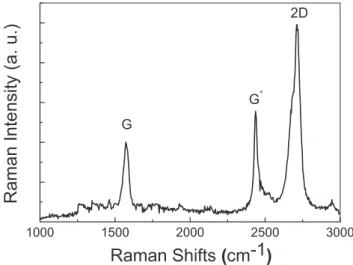
Figure 2 shows the Raman spectrum of the transferred gra-phene, which reveals peaks at 1569, 2435 and 2711 cm−1. The peaks located at 1569 and 2711 cm−1 can be attributed to the G and 2D modes of the graphene, respectively, which is con-sistent with previous studies [20, 14]. The number of layers in the transferred graphene is associated with the intensity ratio of the 2D to G modes. The Raman intensity ratio of the 2D to G modes is found to be 1:2.5, indicating the monolayer nature of graphene [21]. The peak located at 2435 nm is associated to G* Raman band. The G* Raman band reveals the defect activated peak in the Raman Spectrum [22]. However, the D
Figure 1. Schematic diagram of the fabricated graphene/AlGaN/ GaN Schottky photodetector.
Figure 2. Raman spectrum of graphene layer transferred onto the AlGaN/GaN substrate.
mode corresponding to 1346 cm−1 does not appear in the spec-trum, which suggests that the transferred graphene contains few defects [23, 24]. Moreover, the presence of G* band at 2435 nm indicating defects exist in the transferred graphene.
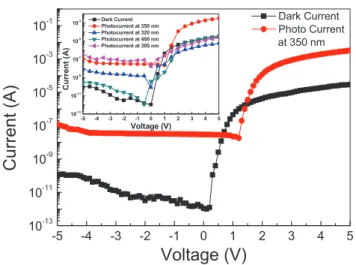
The typical room-temperature I–V characteristics of the graphene/AlGaN/GaN Schottky PD under dark and illu-minated conditions at 350 nm are depicted in figure 3. The fabricated PD shows non-linear behaviour, suggesting that the Schottky barrier is established between the Au electrode/ mono layer graphene and AlGaN/GaN.
The dark current exponentially increases with an increase in the reverse bias, and reaches 9.4 × 10⁻¹¹ A at a bias voltage of −5 V. It is clearly seen from the figure that the dark cur-rent is slightly enhanced above −3 V reverse bias and is found to be increased by 1 to 2 orders of magnitude, which may be considered as a soft breakdown. However, the photocur-rent under 350 nm monochromatic illumination with UV light is observed to be relatively constant up to the bias voltage of −4 V and the photocurrent value is found to be around 3.51 × 10⁻⁸ A. The photocurrent measured below and above 350 nm is found to decrease suggesting that less number of photo carriers is generated and even at 400 nm, photocurrent is very close to dark current as is shown in the inset. However, at 300 nm, photocurrent is marginally increased, there might be more light is absorbed on both AlGaN and GaN layers and produced large number of photo generated carriers.
The turn-on voltage of the fabricated device was about 1.7 V. The photo-to-dark current contrast ratio was found to be more than three orders of magnitude.
The ideality factor and barrier height, which represent characteristic parameters of the Schottky PD, were extracted from the forward I–V characteristics by fitting the ln(I ) versus
V curves using thermionic emission theory. Figure 4 repre-sents the ln(I ) versus V curve of the graphene/AlGaN/GaN Schottky PD.
It is not feasible to obtain an adequate description from the forward I–V curve using a single-diode model. Therefore, an equivalent circuit of two Schottky diodes connected
back-to-back in series was used, as schematically demon-strated in figure 5; diode 1 represents the Schottky contact between Au/graphene and the AlGaN barrier layer, whereas diode 2 models the heterojunction of AlGaN and GaN [25].
According to the thermionic emission model, the reverse saturation current of the two diodes can be written as follows:
⎡ ⎣ ⎢ ⎛⎝⎜ ⎞⎠⎟ ⎤⎦⎥ = − I I qV n kT exp 1 , s1 1 1 (1) where V1 is the voltage across diode 1, n1 is the ideality factor of diode 1, k is the Boltzmann constant, and T is the temper-ature. Is1 can then be expressed as follows:
φ = ∗ ⎛− ⎝⎜ ⎞ ⎠⎟ I AA T q kT exp , s1 2 b1 (2) where q is the electron charge, A is the effective Schottky contact area, A* is the Richardson constant (35.8 × 10⁵
Figure 3. Typical room-temperature I–V characteristics of the graphene/AlGaN/GaN Schottky photodector under dark and illuminated conditions (Inset shows photocurrent above and below 350 nm).
Figure 4. Fitted forward bias ln(I ) versus V curve of the graphene/ AlGaN/GaN Schottky photodector.
Figure 5. The possible energy band diagram of the graphene/ AlGaN/GaN Schottky photodetector modelled as two diodes connected back-to-back in a series equivalent circuit.
M Kumar et al
4 A·cm−2·K−2 [26]), and φ
b1 is the effective barrier height of diode 1. The current through the reverse-biased diode 2 can then be expressed as:
⎡ ⎣ ⎢ ⎛⎝⎜ ⎞⎠⎟ ⎤⎦⎥ = − I I qV n kT exp 1 , s2 2 2 (3) where V2 is the applied voltage across diode 2. Is2 can then be expressed as follows: φ = ∗ ⎛− ⎝⎜ ⎞ ⎠⎟ I AA T q V kT exp , s2 2 b2 2 (4) where φb2 is the barrier height of diode 2. By applying a Taylor series first-order correction, the above equation can be expressed as: ⎡ ⎣ ⎢ ⎛⎝⎜ ⎞⎠⎟⎤ ⎦ ⎥ = I I q V n kT exp , s2 2 2 (5) where the following equations hold:
= ∂Φ ∂ n 1 , V 2 B2 2 (6) φ = ∗ ⎛− ⎝⎜ ⎞ ⎠⎟ I AA T q kT exp 0 . s2 2 b2( ) (7) Here, φb2(0) is the barrier height of diode 2 at zero bias, and n2 represents the effective ideality factor of diode 2. The Chen model [25] suggests that the effective ideality factor n2 indicates the degree of barrier height φb2 change due to the change of voltage across it. A larger value of n2 denotes a smaller change of barrier height. By using these equations, the para meters Is1, Is2, n1, and n2 can be obtained from the forward I–V measurements by linearly fitting the ln(I ) versus V curve in figure 4. More specifically, the parameters Is1 and n1 can be obtained by linearly fitting the ln(I ) versus V curve at a low voltage. The slope provides the information of n1, whereas the intercept of the fitted straight line yields Is1. On the other hand, the parameters Is2 and n2 can be obtained from the linear fit of the ln(I ) versus V curve at an intermediate voltage regime. The product of A and A* in Equations (2) and (7) is not precisely
known because the experimental values of the Richardson con-stant are typically lower than the ideal value, and the effective contact area can be subjected to small variation from point to point. Therefore, in order to determine the values of φb1 and φb2(0) from the fitting values of ln(Is1) and ln(Is2) without using AA*, the subsequent procedure was adopted.
First, the built-in potential across the AlGaN barrier layer at zero bias can be obtained from the following equation [27]:
( ) ( ) φ φ ( ) − = = − ⎛ ⎝⎜ ⎞ ⎠⎟ I I V q KTn ln ln 0 . s2 s1 0 1 b1 b2 (8) The first part of the equation derives from the difference of equations (1) and (7), and Is1 and Is2 are directly obtained from the two linear fits. The obtained values of Is1, Is2, n1, and n2 are 3.04 × 10⁻¹⁶ A, 1.63 × 10⁻⁶ A, 1.57, and 31.32, respectively. It should be noted that V(0) is associated with the difference
between the positive surface polarization charge +σ and the density ND of the AlGaN/GaN 2DEG at zero bias:
( )= σ− V q N C 0 D, AlGaN (9) where C = ε ε d
AlGaN 0 AlGaN is the barrier layer capacitance per
unit area, d is the barrier layer thickness (30 nm), and the relative dielectric permittivity for AlxGa1−xN with an Al concentration of 25% is determined by using the equa-tion ε( )x = −0.5x+9.5, which yields εAlGaN = 9.375. The value of ND can be obtained by calculating the value of V(0) from the fitting results of equation (8) and the σ value from the C–V analysis (σ = 7.86 × 1011 cm−2).
At this stage, the Fermi energy can be expressed as follows [28]: π = + ∗ E E x m x n x 0 S , F 0 2 ( ) ( ) ( ) ( ) (10) where the ground sub-band level of the 2DEG is given by:
( ) ( ) ( ) ( ) π ε ε =⎪⎪⎧ ∗ ⎪⎪ ⎨ ⎩ ⎫ ⎬ ⎭ E x e m x n x x 9 8 . S 0 2 0 2 3 (11) The Fermi level position with respect to the GaN conduction band minimum (ECmin) at zero bias can be expressed as a func-tion of ND [29]: ( ) π π ε ε − = + ⎧⎨ ⎩ ⎫ ⎬ ⎭ E E qm N q q m n 0 1 9 8 8 , F Cmin 2 eff D 2 0 AlGaN eff 2 3 D 2 3 (12) where is the reduced Planck’s constant and meff is the 2DEG effective mass (meff = 0.22me). According to the band struc-ture (illustrated in figure 5), the barrier height of diode 2 is:
φb2( )0 = ∆ −Ec [ ( )EF0 −ECmin],
(13) where ∆EC = 0.34 eV is the Al0.25Ga0.75N/GaN conduction band offset. The barrier height φb1 of diode 1 can be obtained from equation (8). By applying the above procedures, the barrier heights φb1 and φb2 can therefore obtained as 1.14 and 0.228 eV, respectively.
The possible energy band diagram of the graphene/ AlGaN/GaN Schottky PD is depicted in figure 5. Because of the contact potential that results from the difference of the work function of the two materials, electrons accumulate on the graphene side, and band bending in AlGaN/GaN forms the Schottky barrier in under dark conditions. The electron affinity for Al0.25Ga0.75N is about 2.7 eV [30], and the work function of the graphene sheet is known to be 4.5 eV below the vacuum level [31]. Thus, when AlGaN is in contact with the graphene, it is energetically favourable for the photogen-erated electrons to be transferred from the conduction band of AlGaN to the graphene. The graphene side is expected to receive a smaller accumulation of electrons owing to its high carrier mobility. On the other hand, under illumination conditions, AlGaN/GaN absorbs the UV incident light, and graphene serves as a transparent carrier collector. The inci-dent UV light energy (which is larger than the energy gap of J. Phys. D: Appl. Phys. 49 (2016) 275105
AlGaN/GaN) is absorbed, and thus electron–hole pairs are generated and rapidly separated by the built-in electric field at the graphene/AlGaN interface.
It should be noted that some impurities may originate from the chemicals used to release the graphene sheet from the Cu foil, which may exist at the graphene/AlGaN interface. Moreover, desorption of H2O molecules can be induced on graphene during illumination, resulting in trapped electrons that may be released to the graphene. The work function of graphene is reduced under UV illumination, which will lower the Schottky barrier height and increase the Fermi level [32, 33]. The separated electrons can then easily move to the quantum well at the AlGaN/GaN interface. It should be noted that because of the excellent transport properties of graphene, the fabricated graphene/AlGaN/GaN-based Schottky UV PD should have larger incident light absorption efficiency than the metal-based AlGaN/GaN Schottky UV PD. This merit makes the graphene/AlGaN/GaN Schottky UV PD a promising can-didate for potential applications in the large-scale integration of GaN technologies.
The responsivity of the graphene/AlGaN/GaN Schottky PD is shown in figure 6. A small hump at 300 nm and a clear
peak at 350 nm appear in the spectrum; these features are associated with the intrinsic transitions above the band edges of AlGaN and GaN, respectively. The estimated responsivities are obtained as 0.56 and 0.079 A W−1, respectively, at a bias of −2 V. The cut-off wavelength of the graphene/AlGaN/GaN Schottky PD is in good agreement with the band gap energy of Al0.25Ga0.75N and GaN [34].
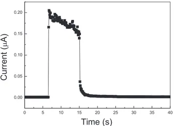
Figure 7 presents the time dependent photocurrent of the graphene/AlGaN/GaN Schottky UV PD illuminated by a 350 nm with a power density of 36 μW and chopper frequency
of 390 Hz at a bias voltage of −2 V. When light is turned on, the PD current increases rapidly from initial value of 1.11 nA to 0.205 μA at around 2 s. Once the light is switched off, the
photocurrent decreased and returns to a low value at a fast recovery process fist and then slow recovery process. The fast recovery time is estimated about 0.1 s and slowly recovery time to the initial value within about 13.7 s. The obtained raising and recovery time response of the graphene/AlGaN/ GaN Schottky UV PD is comparable to UV PD based on colloidal ZnO quantum dot-graphene nanocomposites [35].
4. Conclusion
A CVD-grown monolayer graphene-based Schottky PD was successfully fabricated on an AlGaN/GaN template. The I–V characteristics demonstrate a rectifying behaviour, which suggests that the Schottky barrier was indeed achieved at the interface. The graphene/AlGaN/GaN Schottky PD device exhibits low dark current and a large photo-to-dark contrast ratio. Moreover, the graphene/AlGaN/GaN Schottky PD exhibits a responsivities of 0.56 A W−1 at 300 nm and 0.079 A W−1 at 350 nm at a bias of −2 V. The Schottky parameters were evaluated using an equivalent circuit of two diodes connected back-to-back in series. The obtained results demonstrate that graphene can be successfully used as a transparent electrode in AlGaN/GaN-based PDs. Furthermore, the obtained results suggest that the transparent, conductive graphene electrode may be integrated into existing GaN-based technologies.
Acknowledgments
This research was supported by the Basic Science Research Program (2015R1C1A1A02037326) and the Nano-material Technology Development Program (2009-0082580) through the National Research Foundation of Korea (NRF) funded by the Ministry of Science, ICT, and Future Planning. It was also supported by the 2016 KU Brain Pool of Konkuk University.
References
[1] Razeghi M and Rogalski A 1996 J. Appl. Phys. 79 7433
[2] Ozbay E, Biyikli N, Kimukin I, Tut T, Kartaloglu T and Aytur O 2004 IEEE J. Quantum Electron. 10 742
[3] Pearton S J, Zolper J C, Shul R J and Ren F 1999 J. Appl.
Phys.86 1
[4] Kuryatkov V V, Borisov B A, Nikishina S A, Kuchinskii V I, Sokolovskii G S, Song D Y and Holtz M 2006 J. Appl.
Phys.100 096104
Figure 6. Spectral responsivity of the graphene/AlGaN/GaN Schottky photoditector.
Figure 7. Time response of the graphene/AlGaN/GaN Schottky photoditector.
M Kumar et al
6 [5] Chang K H, Sheu J K, Lee M L, Tu S J, Yang C C, Kuo H S,
Yang J H and Lai W C 2010 Appl. Phys. Lett. 97 013502
[6] Jiang H and Egawa T 2007 Appl. Phys. Lett. 90 121121
[7] Malinowski P E et al 2011 Appl. Phys. Lett. 98 141104
[8] Novoselov K S, Geim A K, Morozov S V, Jiang D, Zhang Y, Dubonos S V, Grigorieva I V and Firsov A A 2004 Science
306 666
[9] Kim K S et al 2009 Nature 457 706
[10] Kim R H et al 2011 Nano Lett. 11 3881
[11] Tongay S, Lemaitre M, Miao X, Gila B, Appleton B R and Hebard A F 2012 Phys. Rev. X 2 011002
[12] Shivaraman S, Herman L H, Rana F, Park J and Spencer M G 2012 Appl. Phys. Lett. 100 18311
[13] Tongay S, Lemaitre M, Schumann T, Berke K, Appleton B R, Gila B and Hebard A F 2011 Appl. Phys. Lett. 99 102102
[14] An Y, Behnam A, Pop E and Ural A 2013 Appl. Phys. Lett.
102 013110
[15] Miao X, Tongay S, Petterson M K, Berke K, Rinzler A G, Appleton B R and Hebard A F 2012 Nano Lett. 12 2745
[16] Shao D, Yu M, Sun H, Hu T, lian J and Sawyera S 2013
Nanoscale5 3664
[17] Ye Y et al 2011 J. Mater. Chem. 21 11760
[18] Yi J, Lee J M and Park W I 2011 Sensors Actuators B 155 264
[19] Babichev A V, Zhang H, Lavenus P, Julien F H, Egorov A Y, Lin Y T, Tu L W and Tchernycheva M 2013 Appl. Phys.
Lett.103 201103
[20] Xu Q, Cheng Q, Zhong J, Cai W, Zhang Z, Wu Z and Zhang F 2014 Nanotechnology 25 055501
[21] Fu X W, Liao Z M, Zhou Y B, Wu H C, Bie Y Q, Xu J and Yu D P 2012 Appl. Phys. Lett. 100 223114
[22] Kaniyoor A and Ramaprabhu S 2009 Phys. Rep. 473 51
[23] Lin F, Chen S W, Meng J, Tse G, Fu X W, Xu F J, Shen B, Liao Z M and Yu D P 2014 Appl. Phys. Lett.
105 073103
[24] Kumar M, Noh Y, Polat K, Okyay A K and Lee D 2015 Solid
State Commun.224 37
[25] Chen C H, Baier S M, Arch D K and Shur M S 1988 IEEE
Trans. Electron Devices 35 670
[26] Lv Y, Lin Z, Corrigan T D, Zhao J, Cao Z, Meng L, Luan C, Wang Z and Chen H 2011 J. Appl. Phys. 109 074512
[27] Fisichella G, Greco G, Roccaforte F and Giannazzo F 2014
Nanoscale6 8971
[28] Shur M S 1998 Mater. Res. Soc. Symp. Proc. 483 15
[29] Ambacher O et al 1999 J. Appl. Phys. 85 3222
[30] Arehart A R, Allerman A A and Ringel S A 2011 J. Appl.
Phys.109 114506
[31] Nourbakhsh A, Cahtoro M, Hadipour A, Voseh T,
Veen M H V D, Heyns M M, Sels B F and Gendt S D 2010
Appl. Phys. Lett.97 163101
[32] Park P S, Reddy K M, Nath D N, Yang Z, Padture N P and Rajan S 2013 Appl. Phys. Lett. 102 153501
[33] Das A et al 2008 Nat. Nanotechnol. 3 210
[34] Kumar M, Lee C Y, Sekiguchi H, Okada H and Wakahara A 2013 Semicond. Sci. Technol. 28 094005
[35] Son D I, Yang H Y, Kim T W and Park W I 2013 Appl. Phys.
Lett.102 021105