Effect of Electron Radiation on Electrical Parameters of Zn/n-Si/Au-Sb and
Zn/ZnO/n-Si/Au-Sb Diodes
Article in Journal of Radioanalytical and Nuclear Chemistry · January 2019 DOI: 10.1007/s10967-018-06401-9 CITATION 1 READS 142 4 authors, including:
Maryam abdolahpour salari Ataturk University 16PUBLICATIONS 5CITATIONS SEE PROFILE Mustafa Sağlam Ataturk University 108PUBLICATIONS 1,749CITATIONS SEE PROFILE Baltakesmez Ali Ardahan University 6PUBLICATIONS 3CITATIONS SEE PROFILE
https://doi.org/10.1007/s10967-018-06401-9
Effect of electron radiation on electrical parameters of Zn/n‑Si/Au–Sb
and Zn/ZnO/n‑Si/Au–Sb diodes
M. A. Salari1 · M. Sağlam1 · A. Baltakesmez2 · B. Güzeldir1
Received: 11 November 2018 / Published online: 2 January 2019 © Akadémiai Kiadó, Budapest, Hungary 2019
Abstract
In this study, RF-magnetron sputtered ZnO thin film as an interlayer was used to improve radiation tolerance of the Schottky diodes. The structural and optical measurements showed that the ZnO thin films have hexagonal crystal structure with prefer-ential c-axis orientation, 20.39 nm grain sizes and 3.15 eV bandgap. The electrical parameters such as ideality factor, barrier height and series resistance of Zn/n-Si/Au–Sb and Zn/ZnO/n-Si/Au–Sb diodes were calculated before and after electron radiation at 25, 50 and 75 gray doses. Deviation values of the parameters showed that the ZnO as an interlayer caused to improved radiation tolerance of the diodes.
Keywords Zinc oxide · Electron radiation · Schottky diode · Heterojunction · Barrier height
Introduction
The simplicity of the construction of metal–semiconductor structures and the determinability provides a wide field of use in the electronics industry [1, 2]. Recently, researchers have been focused on how the naturally occurring or artifi-cially created interlayer between the metal and the semicon-ductor affects the electrical properties and physical param-eters of the contacts in a high radiation environment [3–5].
The choice of functional semiconductor layer using in the fabrication of (opto)electronic device plays an important role in the life-time [6], working stability [7] and efficiency [8] of the device. Therefore, ZnO has potential to use in the (opto) electronic field such as surface acoustic wave device [9], pyroelectric device [10], transparent conducting electrode [11], light emitter [12], photosensitizer [13], gas sensor [14], solar cell [15] and thin-film transistor [16].
ZnO is a very important n-type semiconductor in this field because it has crucial properties such as direct and wide band gap in the near-UV spectral region (3.37 eV)
[17], a large free-exciton binding energy (63 meV) [18], large piezoelectric constant [19], strong luminescence [20], sensitivity of surface conductivity [21], nonlinear resistance [22], large nonlinear optical coefficient [23], high thermal conductivity [24], amenability to wet chemical etching [25] and chemical/physical/thermal stability [26]. Furthermore, for more advanced applications, radiation tolerance capa-bility of the ZnO is a critical property, which is important for the device applications in a high radiation environment. Thus, the radiation tolerance capability of the ZnO allows it to be preferred in applications such as radiation sensors [27], nuclear reactors [28], X-ray imagers [29], and particle accelerators [30].
For example, Lv et al. [31] have reported that the ener-getic particle radiation resistance of the ZnO can be tuned via native defects. Thus, the pre-existed Zni, and VO native defects in ZnO play the lead role while defects of Oi and VZn have weak influences upon H radiation-resistance. On the other hand, Angup et al. [32] have used vertically aligned ZnO nanorods as potential scintillator material for radiation detectors. According to the their study, the ZnO nanorods can be used as scintillator materials which offer not only fast scintillation response but also high spatial resolution for future radiation detectors. In another study, Sahare et al. [33] have reported that a ZnO nanowire/Si heterojunction based sensor has a high speed response with a highly linear sensitivity and very quick recovery time for UV radiation. Besides, Narita et al. [34] have fabricated a Pt/ZnO Schottky * B. Güzeldir
1 Department of Physics, Faculty of Sciences, University
of Atatürk, 25240 Erzurum, Turkey
2 Department of Electricity and Energy, Technical Scientific
Vocational School, Ardahan University, 75000 Ardahan, Turkey
photodiode based on the ZnO single crystal substrates pre-pared by the hydrothermal growth method. Unfortunately, dark currents of sample irradiated with 1015 protons/cm2 increased and the behavior of the forward currents signifi-cantly changed. In another study, the radiation resistant ZnO thin films were used for the efficiency enhancement of GaAs photovoltaics. In this study, Su et al. [35] have demonstrated that the cells coated with the radiation resistant ZnO thin films exhibited less efficiency decay than the devices without such treatment. Under the maximum proton flux of 1013 cm2, the conversion efficiency decay reduced to 69.8%, while the solar cells without ZnO thin films showed an efficiency decay of 83.1%. Briefly, all these and similar studies show that the ZnO as a transparent semiconductor is preferred for stability and long life-time of (opto)electronic devices in a radiation environment.
In this study, Zn/n-Si/Au–Sb as reference and Zn/ZnO/n-Si/Au–Sb diodes were fabricated and exposed to electron irradiation at 25, 50 and 75 gray. The diodes were charac-terized by current–voltage (I–V) measurements in order to better understand the effect of the particle irradiation.
Experimental
n-type Si substrates were cleaned as following: Firstly, the RCA1 and RCA2 cleaning procedures were used to remove difficult surface contamination. (i.e. 10 min boil in NH3 + H2O2 + 6H2O followed by HCl + H202 + 6H2O at 60 °C), secondly, the native oxide on the front surface of the n-Si substrates was removed in 10 vol.% HF + H2O solution and finally the substrates were rinsed in deionized water for 30 s. The ZnO thin films were deposited on the n-Si substrates by RF magnetron sputtering from a ZnO target (purity: 99.99%) at base pressure of 2.0 × 10⁻⁶ Torr. The sputtering power is 60 W and the deposition tempera-ture is 200 °C. The structural properties and surface mor-phology of the ZnO thin films were analyzed by the X-ray diffractometer (XRD) (X’Pert PRO, λ = 0.154 nm) using Cu-Kα radiation, the scanning electron microscopy (SEM) (Zeiss Sigma 300) and the atomic force microscope (AFM) (Hitachi 5100 N), respectively. The UV–visible spectro-photometer (Lambda35) was used to optical measurements. From the absorbance (A) measurement, absorbance spectra is converted to absorption coefficients by using the formula (1) in order to find the bandgaps of the thin films from the 𝛼2 versus hv plots [the formula (2)],
(1) T= (1 − R) 2exp(− 𝛼t) (1 − R2) exp(− 2𝛼t) = exp(− A) (2) 𝛼hv= K(hv − Eg)1∕2
where T the transmittance, R the reflectance, 𝛼 the absorp-tion coefficient, t the film thickness, hv the incident photon energy, Eg the bandgap energy of the samples and K the constant. The film thickness was measured using a surface profilometer (KLA Tencor P7).
When the ZnO thin film characterization process is finished, two groups of diodes were prepared on the n-Si substrates at the same conditions. Au–Sb alloy ohmic con-tacts were deposited on the mat surface of n-Si substrate by thermal evaporating. The ZnO thin films as interlayer were deposited on the one group of n-Si substrates by RF-magne-tron sputtering technique. Finally, Zn metal was evaporated on the n-Si and the ZnO/n-Si substrates by thermal evapo-rating technique to obtain Zn/n-Si/Au–Sb and Zn/ZnO/n-Si/ Au–Sb diodes, respectively. Each of the two group diodes were put in the electron radiation tester (The Varian Trilogy model of LİNAC) and exposed to electron irradiation up 25–75 gray with 25 gray steps at room temperature, respec-tively. Before and after specified doses electron irradiation, the I–V measurements of Zn/n-Si/Au–Sb and Zn/ZnO/n-Si/Au–Sb diodes were carried out by using Keitley 487 Picoammeter/Voltage Source at room temperature.
Results and discussion
Characterization of the ZnO thin film
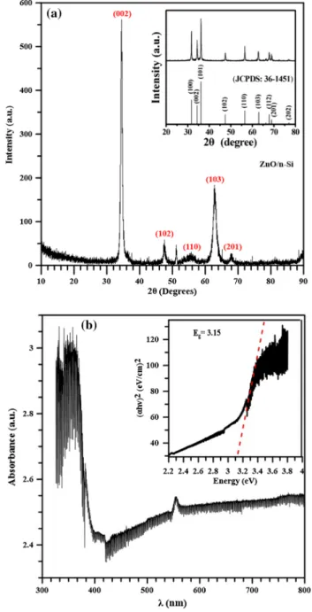
Figure 1a shows that the XRD pattern of RF-sputtered ZnO thin films on the Si substrate The peaks of (002) (d = 2.59 Å), (102) (d = 1.91 Å), (110) (d = 1.65 Å), (103) (d = 1.47 Å) and (112) (d = 1.38 Å) of the ZnO film coin-cide very well with the standard peaks of the ZnO phase and with previously reported studies [36, 37]. It can be also seen in the figure that the ZnO thin film c-axis oriented with predominant XRD peak centered at 2θ value of 34.1° cor-responding to (002) plane. Thus, the resulting XRD patterns can be attributed to the ZnO hexagonal wurtzite structure with verified parameters in JCPDS Card No. 36-1451. For the (002) predominant peak, the crystal size of the thin film was calculated by using the Scherrer formula [37] and it was found 20.39 nm.
Figure 1b shows the absorption spectra of the ZnO thin film sputtered on the glass substrate. Besides, the absorbance data were transformed to the absorption coefficient (α2) and figured graph of the α2 versus energy of incident photons is given inset figure in Fig. 1b. The sharp absorption edge of the ZnO thin film confirms structural quality of the film. The band gap (Eg) of the ZnO film was calculated as 3.15 eV, which is compatible with the reported bandgap (~ 3.37 eV) of the ZnO film prepared by different processes.
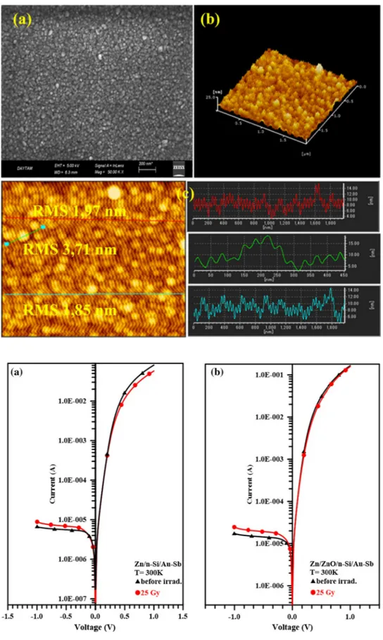
The morphological properties of the films such as the shape and size of the grains in the films and the
distribution of these were determined by the SEM image in Fig. 2a and the AFM image in Fig. 2b. It is clearly seen that the ZnO thin film formed with crystal grains having different sizes and these grains clustered some place on the surface of the films. Besides, the grain sizes of the films, as seen in SEM image, have approximate value of the grain size calculated from the XRD analysis. Root mean square (RMS) roughness obtained by the AFM measurement is between 1 and 4 nm, which is a very suitable range to obtain smooth surface, as seen in Fig. 2c.
Irradiation effect at I–V characteristics of Zn/n‑Si/ Au–Sb and Zn/ZnO/n‑Si/Au–Sb diodes
The current in the uniform metal–semiconductor interface can be expressed as follows according to the thermionic emission [38]:
where I0 is the saturation current given by
q is the electron charge, V is the forward-bias voltage, A is the effective diode area, k is the Boltzmann constant, T is the absolute temperature, A* is the effective Richardson constant of 112 A cm−2 K−2 for n-type Si, 𝛷
ap is the zero bias appar-ent barrier height and n is the ideality factor. From Eq. (4), ideality factor n can be written as
The ideality factor, which is an important parameter that determines the quality of the diode, is unitless and it should be 1 for an ideal diode. The deviation from the ideal I–V characteristics can be due to the presence of an indefinable interfacial layer that affecting the interface states [39].
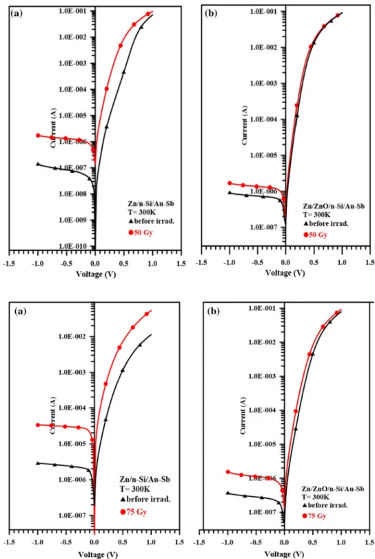
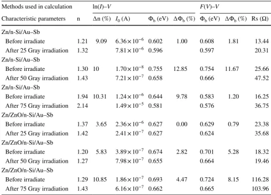
Figures 3, 4 and 5 present the forward and reverse bias I–V characteristics of Zn/n-Si/Au–Sb and Zn/ZnO/n-Si/ Au–Sb diodes before and after irradiation at specific doses. Figure 3a, b show the I–V characteristics of reference and ZnO interlayered diodes exposed to 25 Gy radiation, respec-tively. In the diodes, there is a very small and comparable increment in the reverse bias current after exposure to radia-tion. However, there are significantly changes in the forward bias characteristics. As seen in the figure, the radiation effect in the reference diode showed itself as an increasing series resistance, while the I–V characteristic of diode with the ZnO interlayer almost unchanged. This result demonstrates that unshielded electronic devices are easily affected by low radiation doses. Figure 4a, b show the I–V characteristics of the diodes exposed to 50 Gy radiations, respectively. Fur-thermore, when the radiation dose is increased to 50 Gy, a serious reaction occurred in the reference diodes, as seen in Fig. 4a. Interestingly, the reverse bias current has incre-ment by more than 10 times in the reference diode while the increment of the reverse bias current of diode formed with the ZnO interlayer is very small. Furthermore, the forward bias characteristic of the reference diode has also changed with increasing series resistance. However, the diode formed with the ZnO interlayer has exhibited a stable forward bias (3) I= I0exp ( qV nkT )[ 1− exp ( −qV kT )] (4) I0 = A A∗T2 exp ( −q𝛷ap kT ) (5) n= q kT ( dV d ln I )
Fig. 1 a The XRD pattern and b the optical absorption plot of the ZnO thin film grown on the n-Si and glass substrates, respectively
characteristic with a reasonable change. Figure 5a, b show the I–V characteristics of the diodes exposed to 75 Gy radia-tions. While the radiation dose was 75 Gy, the effect on
the operating characteristics of the diodes became more pronounced. In this radiation dose, the reverse bias current and the series resistance of the reference diode have further Fig. 2 a SEM and b AFM
images of the ZnO thin film grown on the n-Si substrate
Fig. 3 The forward and reverse bias I–V characteristics before and after 25 gray electron radia-tion doses, a the Zn/n-Si/Au–Sb and b the Zn/ZnO/n-Si/Au–Sb
increased. On the other hand, the change in operating char-acteristic of the diode formed with ZnO interlayer is evident but it is comparable to the change in the reference diode exposed to 25 Gy radiations. These results can be interpreted that the ZnO interlayer improves the operating stability of the device nearly 3 times.
After these measurements, the ideality factor, barrier height and saturation current were calculated for both diode
structures and the results are given in Table 1. As seen in Table 1, the radiation generally caused an increment in the ideality factor and a decrease in the barrier height. The increment in the ideality factor for both diode structures with increasing radiation dose is mainly due to the defects, trap-ping and recombination centers formed with the radiation in the interface. Furthermore, image force effect, tunneling, interface impurities and natural oxide interface are the Fig. 4 The forward and reverse
bias I–V characteristics before and after 50 gray electron radia-tion doses, a the Zn/n-Si/Au–Sb and b the Zn/ZnO/n-Si/Au–Sb
Fig. 5 The forward and reverse bias I–V characteristics before and after 75 gray electron radia-tion doses, a the Zn/n-Si/Au–Sb and b the Zn/ZnO/n-Si/Au–Sb
possible factors for strengthens the effects of the radiation. On the other hand, The decrease of the barrier height after the radiation is due to increasing interface defect density and consequently the increment in the number of carriers trapping [40]. Thus, tunneling might be dominant current mechanism because the current transport mechanism of the diodes is not complying with the thermionic emission theory as seen in the results [41, 42].
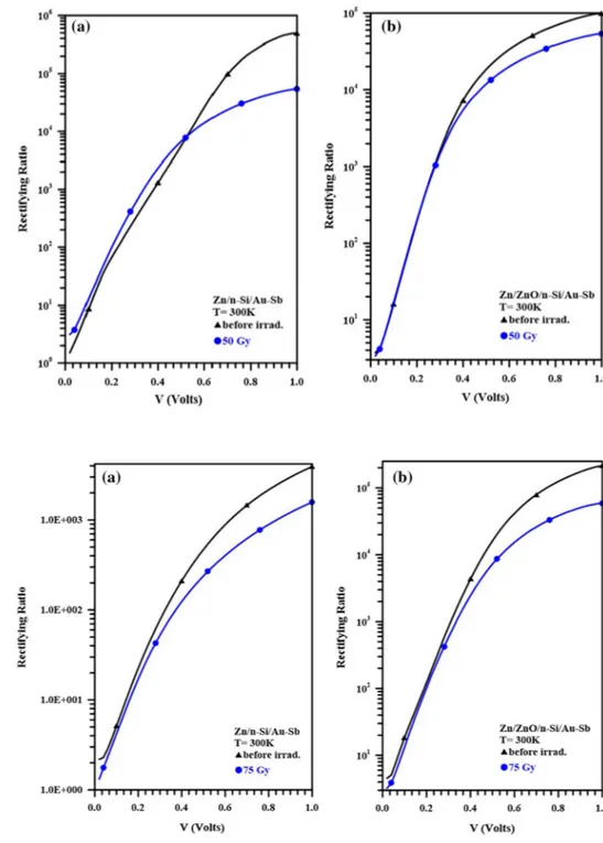
Figures 6, 7 and 8 show rectification graphs with respect to applied voltage for Zn/n-Si/Au–Sb and Zn/ZnO/n-Si/ Au–Sb diodes before and after expose to radiation. As clearly seen in the figure that the rectification current of the diode formed with ZnO interlayer has slightly changed after the radiation. This situation can be attributed to improving radiation tolerance of the metal–semiconductor interface [39].
Table 1 The key parameters obtained from the I–V characteristics of the Zn/n-Si/ Au–Sb and Zn/ZnO/n-Si/Au–Sb diode structures before and after 25, 50 and 75 Gray doses
Methods used in calculation ln(I)–V F(V)–V
Characteristic parameters n ∆n (%) I0 (A) Φb (eV) ∆Фb (%) Φb (eV) ∆Фb (%) Rs (Ω)
Zn/n-Si/Au–Sb
Before irradiate 1.21 9.09 6.36 × 10⁻⁶ 0.602 1.00 0.608 1.81 13.44
After 25 Gray irradiation 1.32 7.81 × 10⁻⁶ 0.596 0.597 20.31
Zn/n-Si/Au–Sb
Before irradiate 1.30 10 1.70 × 10⁻⁸ 0.755 12.85 0.754 11.67 25.66
After 50 Gray irradiation 1.43 7.21 × 10⁻⁷ 0.658 0.666 47.52
Zn/n-Si/Au–Sb
Before irradiate 1.94 10.31 1.24 × 10⁻⁶ 0.644 9.78 0.583 1.20 16.25
After 75 Gray irradiation 2.14 1.49 × 10⁻⁵ 0.581 0.576 36.75
Zn/ZnO/n-Si/Au–Sb
Before irradiate 1.37 3.65 2.36 × 10⁻⁶ 0.627 0.00 0.629 0.79 23.38
After 25 Gray irradiation 1.42 2.41 × 10⁻⁷ 0.627 0.624 35.68
Zn/ZnO/n-Si/Au–Sb
Before irradiate 1.20 5.83 3.89 × 10⁻⁷ 0.674 2.82 0.701 5.28 18.32
After 50 Gray irradiation 1.27 7.98 × 10⁻⁷ 0.655 0.664 19.46
Zn/ZnO/n-Si/Au–Sb
Before irradiate 1.29 10.85 1.86 × 10⁻⁷ 0.693 4.47 0.724 8.15 116.28
After 75 Gray irradiation 1.43 6.16 × 10⁻⁷ 0.662 0.665 103.96
Fig. 6 The rectification current versus voltage plots before and after 25 gray electron radiation doses, a the Zn/n-Si/Au–Sb and b the Zn/ZnO/n-Si/Au–Sb
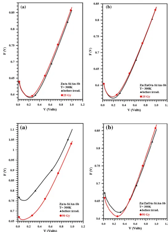
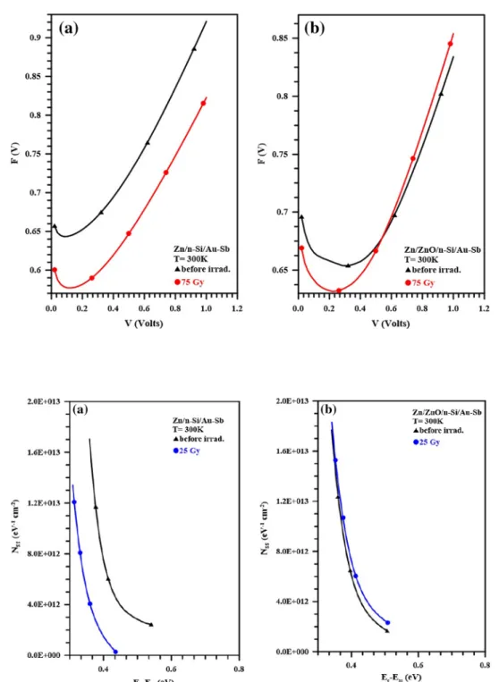
Norde’s function F(V) has been used to obtain the values of barrier height and the series resistance. The F(V) function is defined as [43]:
where I (V) is current obtained from the I–V curve. Graphs of F (V) versus V for the Zn/n-Si/Au–Sb and Zn/ZnO/n-Si/ Au–Sb diodes before and after the radiation are given in Figs. 9, 10 and 11. From the graphs of F (V) versus V, the values of the barrier heights of the diodes can be determined as follows:
(6) F(V) = (V∕𝛾) − (kT∕q) ln(I(V)∕AA∗T2)
where F (Vmin) is the minimum value of F (V) and Vmin is the corresponding voltage. For real contacts (n > 1), the series resistance Rs can be expressed as:
where Imin is the value of the forward current at the voltage Vmin where the function F(V) exhibits a minimum.
The parameters of Zn/n-Si/Au–Sb and Zn/ZnO/n-Si/ Au–Sb diodes were calculated by the Norde method as seen in Table 1. It is observed that the values of series resistance (7) 𝛷b = F(Vmin) + (Vmin∕𝛾) − (kT∕q)
(8) Rs= kT(𝛾 − n)∕qImin
Fig. 7 The rectification current versus voltage plots before and after 50 gray electron radiation doses, a the Zn/n-Si/Au–Sb and b the Zn/ZnO/n-Si/Au–Sb
Fig. 8 The rectification current versus voltage plots before and after 75 gray electron radiation doses, a the Zn/n-Si/Au–Sb and b the Zn/ZnO/n-Si/Au–Sb
increased whereas the barrier height decreased with the radi-ation. This can be interpreted as the reduction of the carrier concentration in the crystal and formation of new carriers in the depletion region. Besides, increasing reverse current is due to the concentration of minority carriers near the junc-tion with lattice defects. Thus, with increasing radiajunc-tion energy, mobility and free carrier concentration decrease by the formation of defect centers such as deep trap, recombina-tion or scattering centers due to shortening the lifetime of the minority carriers [44]. In other words, formation of defects at the interface and then an increment in the interface state
density lead to a reduction in the Schottky barrier height and an increment in the ideality factor.
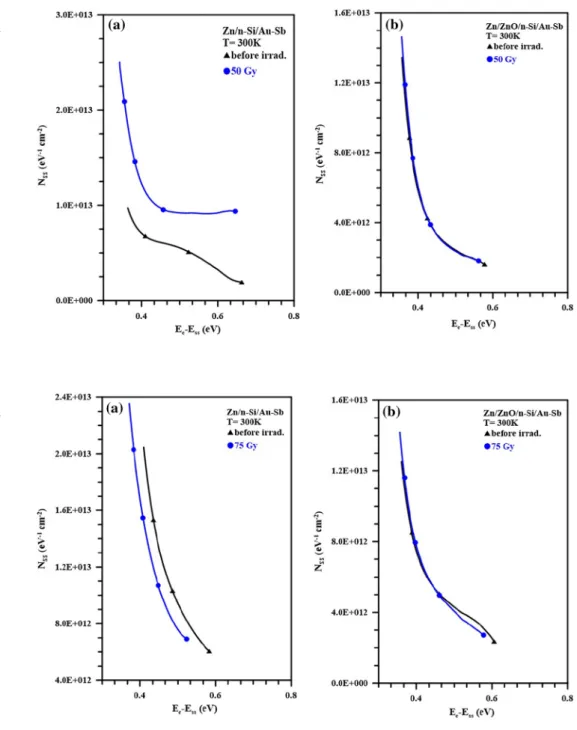
Furthermore, in n-type semiconductors, the energy of interface states Ess with respect to the bottom of the conduc-tion band at the surface of semiconductor and it is given as; The distribution curves of interface state energy of the Zn/n-Si/Au–Sb and Zn/ZnO/n-Si/Au–Sb diodes with respect to the radiation energy are given in Figs. 12, 13
and 14. As can be seen from the figures, the interface (9) Ec− Ess= e(𝛷b− V)
Fig. 9 The F(V)–V plots before and after 25 gray electron radia-tion dose, a the Zn/n-Si/Au–Sb and b the Zn/ZnO/n-Si/Au–Sb
Fig. 10 The F(V)–V plots before and after 50 gray electron dose, a the Zn/n-Si/Au–Sb and b the Zn/ZnO/n-Si/Au–Sb
state density ( Nss ) exponential increased from the band mid-gap towards the top of the conduction band, because of radiation energy. In the same time, the Nss have lightly changed with increasing radiation energy. A changing in the interface state density can be leaded to the decrease in the recombination centers and due to the presence of ZnO layer. Therefore, these changes are based on the changes of interface states of Schottky contacts [45].
Conclusions
In this study, we have prepared the Zn/n-Si/Au–Sb as a reference diode and the Zn/ZnO/n-Si/Au–Sb as a working diode. Investigation of the electrical working stability of the diodes was carried out by the I-V measurements at the different doses of electron radiation. The results showed Fig. 11 The F(V)–V plots before
and after 75 gray electron radia-tion dose, a the Zn/n-Si/Au–Sb and b the Zn/ZnO/n-Si/Au–Sb
Fig. 12 The Nss− (Ec− Ess) plots before and after 25 gray electron radiation doses, a the Zn/n-Si/ Au–Sb and b the Zn/ZnO/n-Si/ Au–Sb
that the Zn/ZnO/n-Si/Au–Sb diodes have reproducible with same parameters, and the Zn/ZnO/n-Si/Au–Sb diode is more stable than the Zn/n-Si/Au–Sb reference diode in the all radiation doses. This result is attributed to the qual-ity of the interface. Because of defects generated by the radiation at the interface, the working stability of Zn/n-Si/ Au–Sb reference diode has deteriorated by increasing ide-ality factor and series resistance with increasing electron radiation energy. However, the radiation-induced defects cannot create between the metal–semiconductor at speci-fied doses. Eventually, the electrical parameters of the Zn/ ZnO/n-Si/Au–Sb diode are indicated that the ZnO thin film
can be used in many (opto)electronic applications for the working stability at the electron radiation.
Acknowledgments We thank to Yılmaz Şahin from Atatürk University for help in exposing electron irradiation measurements.
References
1. Umezawa H, Shikata S, Funaki T (2014) Diamond Schottky bar-rier diode for high-temperature, high-power, and fast switching applications. Jpn J Appl Phys 53:570–576
Fig. 13 The Nss− (Ec− Ess) plots before and after 50 gray electron radiation doses, a the Zn/n-Si/ Au–Sb and b the Zn/ZnO/n-Si/ Au–Sb
Fig. 14 The Nss− (Ec− Ess) plots before and after 75 gray electron radiation doses, a the Zn/n-Si/ Au–Sb and b the Zn/ZnO/n-Si/ Au–Sb
2. Güzeldir B, Sağlam M, Ateş A (2010) Analysis of the electrical characteristics of Zn/ZnSe/n-Si/Au–Sb structure fabricated using SILAR method as a function of temperature. J Alloys Compd 506:388–394
3. Akay D, Efil E, Kaymak N, Orhan E, Ocak SB (2018) Study of frequency dependent characterization: applied gamma-ray irradiation on metal-polymer nanostructure. Radiat Phys Chem 318:1409–1417
4. Aydogan Ş, İncekara Ü, Türüt A (2011) The effects of 12 MeV electron irradiation on the electrical characteristics of the Au/ Aniline blue/p-Si/Al device. Microelectron Reliab 51(12):1–7 5. Uslu H, Yıldırım M, Altındal Ş, Durmuş P (2012) The effect
of gamma irradiation on electrical and dielectric properties of organic-based Schottky barrier diodes (SBDs) at room tempera-ture. Radiat Phys Chem 81:362–369
6. Venkatesan S, Ngo E, Khatiwada D, Zhang C, Qiao Q (2015) Enhanced lifetime of polymer solar cells by surface passiva-tion of metal oxide buffer layers. ACS Appl Mater Interfaces 7(29):16093–16100
7. Dong H, Pang S, Zhang Y, Chen D, Zhu W, Xi H, Chang J, Zhang J, Zhang C, Hao Y (2018) Improving electron extraction abil-ity and device stabilabil-ity of perovskite solar cells using a compat-ible PCBM/AZO electron transporting bilayer. Nanomaterials 720:1–10
8. Liu X, Liu C, Sun R, Liu K, Zhang Y, Wang HQ, Fang J, Yang C (2015) Improved device performance of polymer solar cells by using a thin light-harvesting-complex modified ZnO film as the cathode interlayer. ACS Appl Mater Interfaces 7(34):18904–18912
9. Zhou J, He XL, Wang WB, Zhu Q, Xuan WP, Jin H, Dong SR, Wang DM, Luo JK (2013) Transparent surface acoustic wave devices on ZnO/glass using Al-doped ZnO as the electrode. IEEE Electron Device Lett 34:1319–1321
10. Hsiao CC, Yu SY (2012) Improved response of ZnO films for pyroelectric devices. Sensors 12:17007–17022
11. Sharma V, Kumar P, Kumar A, Surbhi Asokan K, Sachdev K (2017) High-performance radiation stable ZnO/Ag/ZnO multi-layer transparent conductive electrode. Sol Energy Mater Sol Cells 169:122–131
12. Baltakesmez A, Tekmen S, Tüzemen S (2011) ZnO homojunction white light-emitting diodes. J Appl Phys 110:1–7
13. Firdous S (2018) Development and imaging of zinc oxide nanorods as a photosensitizer for the diagnosis and treatment of cancer using lasers. Laser Phys Lett 15:1–8
14. Davydova M, Laposa A, Smarhak J, Kromka A, Neykova N, Nahlik J, Kroutil J, Drahokoupil J, Voves J (2018) Gas-sensing behaviour of ZnO/diamond nanostructures. Beilstein J Nanotech-nol 9:22–29
15. Baltakesmez A, Biber M, Tüzemen S (2018) Inverted planar per-ovskite solar cells based on Al doped ZnO substrate. J Radiat Res Appl Sci 112:124–129
16. Alshammari FH, Nayak PK, Wang Z, Alshareef HN (2016) Enhanced ZnO thin-film transistor performance using bilayer gate dielectrics. ACS Appl Mater Interfaces 8(35):22751–22755 17. Maji TK, Bagchi D, Kar P, Karmakar D, Pal SK (2017) Enhanced
charge separation through modulation of defect-state in wide band-gap semiconductor for potential photocatalysis application: ultrafast spectroscopy and computational studies. J Photochem Photobiol A 332:391–398
18. Su YQ, Zhu Y, Yong D, Chen M, Su L, Chen A, Wu Y, Pan B, Tang Z (2016) Enhanced exciton binding energy of ZnO by long-distance perturbation of doped be atoms. J Phys Chem Lett 7:1484–1489
19. Dai S, Dunn ML, Park HS (2010) Piezoelectric constants for ZnO calculated using classical polarizable core-shell potentials. Nano-technology 21:44507–44515
20. Raji R, Gopchandran KG (2017) ZnO nanostructures with tunable visible luminescence: effects of kinetics of chemical reduction and annealing. J Sci Adv Mater Dev 2:51–58
21. Viespe C, Miu D (2017) Surface acoustic wave sensor with Pd/ ZnO bilayer structure for room temperature hydrogen detection. Sensors 17:1–9
22. Tang C, Jiang C, Lu W, Song J (2013) Nonlinear length dependent electrical resistance of a single crystal zinc oxide micro/nanobelt. Phys Chem Chem Phys 21:1–6
23. Zhang KX, Yao CB, Wen X, Li QH, Sun WJ (2018) Ultrafast nonlinear optical properties and carrier dynamics of silver nano-particle-decorated ZnO nanowires. RSC Adv 8:26133–26143 24. Wu X, Lee J, Varshney V, Wohlwend JL, Roy AK, Luo T (2016)
Thermal conductivity of wurtzite zinc-oxide from first-principles lattice dynamics a comparative study with gallium nitride. Sci Rep 22504:1–10
25. Sahal M, Mari B, Mollar M, Manjon FJ (2010) Zn1-xMgxO
thin films deposited by spray pyrolysis. Phys Status Solidi C 79:2306–2310
26. Farzana R, Rajarao R, Behera PR, Hassan K, Sahajwalla V (2018) Zinc oxide nanoparticles from waste Zn-C battery via thermal route: characterization and properties. Nanomaterials 717:1–12 27. Zhao X, Chen L, HeY Liu J, Peng W, Huang Z, Qi X, PanZ Zhang
W, Zhang Z, Ouyang X (2016) Nanosecond X-ray detector based on high resistivity ZnO single crystal semiconductor. Appl Phys Lett 108:1–4
28. Koike K, Aoki T, Fujimoto R, Sasa S, Yano M, Gonda S, Ishigami R, Kume K (2012) Radiation hardness of single-crystalline zinc oxide films. Phys Stat Solidi 7:1577–1579
29. Samarin SN, Saramad S (2018) Simulation the spatial resolution of an X-ray imager based on zinc oxide nanowires in anodic alu-minium oxide membrane by using MCNP and OPTICS Codes. J Instrum 13(05):1–12
30. Vincke H, Theis C, Roesler S (2011) Induced radioactivity in and around high-energy particle accelerators. Radiat Prot Dosim 146:434–439
31. Lv J, Li C, Liu Y (2016) Oxygen-deficient defects facilitate H radiation resistance in ZnO. Phys Stat Solidi B 254:1–5 32. Angub MCM, Vergara CJT, Husay HAF, Salvador AA, Empizo
MJF, Kawano K, Minami Y, Shimizu T, Sarukura N, Somintac AS (2018) Hydrothermal growth of vertically aligned ZnO nanorods as potential scintillator materials for radiation detectors. J Lumin 203:427–435
33. Sahare PD, Kumar S, Singh F (2018) n-ZnO/p-Si heterojunc-tion nanodiodes based sensor for monitoring UV radiaheterojunc-tion. Sens Actuators A 279:351–360
34. Narita S, Endo H, Chiba T, Sakemi Y, Itoh M, Yoshida H (2014) Characteristics of ZnO Schottky photodiode and effects of high-energy proton irradiation. Phys Stat Solidi A 211:570–573 35. Su BY, Su YK, Tseng ZL, Shih MF, Cheng CY, Wu TH, Wu
CS, Yeh JJ, Ho PY, Juang YD, Chu SY (2011) Antireflective and radiation resistant ZnO thin films for the efficiency enhancement of GaAs photovoltaics. J Electrochem Soc 158:267–270 36. Deshpande VP, Sartale SD, Vyas AN, Ubale AU (2017)
Tempera-ture dependent properties of spray deposited nanostrucTempera-tured ZnO thin films. Int J Mater Chem 7(2):36–46
37. Bachari EM, Baud G, Ben AS, Jacquet M (1999) Structural and optical properties of sputtered ZnO films. Thin Solid Films 348(1):165–172
38. Rhoderick EH, Williams RH (1988) Metal-semiconductor con-tacts, 2nd edn. Oxford University Press, Oxford
39. Sze SM (1981) Physics of semiconductor devices. Wiley Press, New York
40. Krishnan S, Sanjeev G, Pattabi M (2008) Electron irradiation effects on the Schottky diode characteristics of p-Si. B: Beam Interact Mater Atoms 266(4):621–624
1 3
41. Karataş Ş, Türüt A (2006) Electrical properties of Sn/p-Si (MS) Schottky barrier diodes to be exposed to 60 Co γ-ray source. Nucl Instrum Methods Phys Res Sect A 566:584–589
42. Singh R, Arora SK, Kanjilal D (2001) Swift heavy ion irradia-tion induced modificairradia-tion of electrical characteristics of Au/n-Si Schottky barrier diode. Mater Sci Semicond Process 4(5):425–432 43. Norde H (1979) A modified forward I-V plot for Schottky diodes
with high series resistance. J Appl Phys 50:5052–5055
44. Karadeniz S (2007) 60 Co γ-ray irradiation effects on dielectric characteristics of tin oxide films of different thicknesses on n-type Si (1 1 1) substrates. Nucl Instrum Methods Phys Res Sect B 260:571–578
45. Akay D, Karadeniz S, Birkan A, Ocak SB (2018) Effect of gamma-ray irradiation on the electrical characteristics of Al/ C24H12/p-Si nano-structure. Phys Scr 93:1–5
Publisher’s Note Springer Nature remains neutral with regard to jurisdictional claims in published maps and institutional affiliations.