LOW POWER SMART WIRELESS MOBILE ELECTRONIC CONTROL SYSTEM
by
Emin Cihan Anıl
Submitted to the Institute of Graduate Studies in Science and Engineering in partial fulfillment of
the requirements for the degree of Master of Science
in
Electrical and Electronics Engineering
Istanbul Bilgi University 2019
iii
ACKNOWLEDGEMENTS
Thanks to people who supported me during the thesis, I have been motivated. I especially want to thank several people.
First of all, I would like to thank my supervisor, Asst. Prof. Baykal Sarıoğlu for his guide and support. He has given me precious knowledges for both academic life and business life. Also, I would like to thank Asst. Prof. Okan Zafer Batur and Asst. Prof. Revna Acar to attend my thesis committee.
I would like to thank TUBITAK Project No’s: 114E549.
Special thanks to my family which are the most precious people in my life. I am grateful them for believing and always being patient and supportive of me.
ABSTRACT
LOW POWER SMART WIRELESS MOBILE
ELECTRONIC CONTROL SYSTEM
Microsystems which can be placed on the patient with micro size and very low power consumption and will be able to work continuously to monitor the course of the disease are needed in biomedical area. Complementary Metal Oxide Semiconductor (CMOS) technology is preferred for most of biomedical systems due its common usage, design conveniences and low cost.
The design and results of oscillator based capacitive and resistive sensing circuits with low supply voltage and low power consumption are presented for an optically powered biomedical microsystem. The oscillator based sensing circuits are designed and simulated using 180 nm United Microelectronics Corporation (UMC) CMOS technology. Also, the theoretical relationships between the output frequency and sensor resistance/capacitance are derived. For optical microsystem, communication protocols which are pulse width modulation (PWM) and pulse amplitude modulation (PAM) are presented to transmit the data. Arduino Uno is used to represent the microsystem. Raspberry Pi 3B is used as a transmitter. Mutual data transmission is carried out by means of Infrared Radiation (IR) Light Emitting Diode (LED) which is transmitter and phototransistor which is receiver. Thanks to infrared beam, the power consumption of designed circuit is very low. A Graphical User Interface (GUI) is designed on the Raspberry Pi. The Raspberry Pi serves as a control panel and so different data is sent to the receiver.
v
ÖZET
DÜŞÜK GÜÇ TÜKETİMLİ AKILLI
KABLOSUZ MOBİL ELEKTRONİK
KONTROL SİSTEMİ
Biyomedikal alanda, hastalık seyrinin izlenebilmesi adına sürekli çalışacak ve hasta üzerine yerleşimi mümkün olan mikro boyutlu ve çok düşük güç tüketimli mikro sistemlere ihtiyaç duyulmaktadır. Tümler Metal Oksit Yarıiletken (CMOS) teknolojisinin, yaygınlığı ve tasarımı açısından getirdiği kolaylıklar ve düşük maliyeti düşünülerek amaçlanan biyomedikal mikro sistemin kullanımı açısından tercih edilmektedir.
Optik olarak çalışan bir biyomedikal mikro sistem için düşük besleme gerilimi ve düşük güç tüketimi ile osilatör bazlı kapasitif ve dirençli algılama devrelerinin tasarımı ve sonuçları sunulmaktadır. Salıngaç temelli algılama devreleri 180 nm Birleşik Mikroelektronik Şirketi (UMC) CMOS teknolojisi kullanılarak tasarlanmış ve benzetimleri gerçekleştirilmiştir. Ayrıca çıkış frekansı ile algılayıcı direnç/sığa değeri arasındaki teorik eşitlikleri türetilmiştir. Optik mikrosistemde, veri iletimi için darbe genişlik modülasyonu (PWM) ve darbe genlik modülasyonu (PAM) iletişim protokolleri sunulmaktadır. Arduino Uno, mikro sistemi temsil etmek için kullanılmıştır. Raspberry Pi 3B verici olarak kullanılmıştır. Üzerinde bulunan verici kısım olan IR LED ve alıcı kısım olan fototransistör sayesinde karşılıklı veri gönderimi gerçekleşmektedir. Kızılötesi ışın sayesinde, tasarlanan devrenin güç tüketimi çok düşüktür. Raspberry Pi'de bir Grafiksel Kullanıcı Arayüzü (GUI) tasarlanmıştır. Raspberry Pi bir kontrol paneli olarak görev yapar ve böylece alıcıya farklı veriler gönderilir.
TABLE OF CONTENTS
ACKNOWLEDGEMENTS ... iii
ABSTRACT ... iv
ÖZET ... v
LIST OF FIGURES ... viii
LIST OF TABLES ... x
LIST OF ABBREVIATION / SYMBOLS ... xi
1. INTRODUCTION ... 1
2. LOW POWER CMOS OSCILLATOR DESIGNS ... 3
2.1. LC CMOS Cross Coupled Oscillator ... 4
2.2. Relaxation Oscillator ... 8
2.3. Ring Oscillator ... 12
2.4. Comparison of The Designed Low Power CMOS Oscillator ... 16
3. WIRELESS OPTICAL EMBEDDED SYSTEM REALIZATION ... 19
3.1. Transmitter Design ... 20
3.1.1. Raspberry Pi 3B ... 23
3.1.2. Raspberry Pi 3B DAC board ... 24
3.1.3. IR LED ... 26
3.2. Receiver Design ... 28
3.2.1. Arduino Uno ... 29
3.2.2. Phototransistor & Photodiode ... 30
3.3. IR Transmission Between Raspberry Pi 3B and Arduino Uno ... 32
3.4. Experimental Results ... 34
4. RESULTS & CONCLUSION ... 39
5. REFERENCES ... 40
REFERENCES NOT CITED ... 42
vii
APPENDIX B: TRANSMITTER CODE ... 54 APPENDIX C: RECEIVER CODE ... 57
LIST OF FIGURES
Figure 1.1 The block diagram of the all-optical biomedical system ... 2 Figure 2.1 (a) MOSFET cross coupled pair, (b) Equivalent circuit of the cross coupled pair [10] ... 4 Figure 2.2 The circuit diagram of the designed LC CMOS cross coupled oscillator ... 5 Figure 2.3 The circuit diagram of the designed LC CMOS cross coupled oscillator in ADS simulation program ... 6 Figure 2.4 Simulation result of the designed LC CMOS cross coupled oscillator, VDD = 1 V ... 7 Figure 2.5 Power dissipation vs supply voltage graph of the designed LC CMOS cross coupled oscillator, VDD=1 V ... 7 Figure 2.6 The circuit diagram of the designed relaxation oscillator... 9 Figure 2.7 The circuit diagram of the designed relaxation oscillator in ADS simulation program ... 10 Figure 2.8 Simulation result of the designed relaxation oscillator, VDD = 1 V ... 11 Figure 2.9 Power dissipation vs supply voltage graph of the designed relaxation oscillator, VDD=1V ... 11 Figure 2.10 The circuit diagram of the designed ring oscillator ... 12 Figure 2.11 The circuit diagram of the designed ring oscillator in ADS simulation program ... 13 Figure 2.12 Simulation result of the designed ring oscillator, VDD = 0.5 V ... 15 Figure 2.13 Power dissipation vs supply voltage graph of the designed ring oscillator VDD=0.5 V ... 15 Figure 2.14 Comparison of the theoretical and the simulation results for the designed ring oscillator in terms of oscillation frequency value ... 16 Figure 2.15 The layout of the sensing circuit ... 18 Figure 3.1 Wireless optical embedded system realization ... 20 Figure 3.2 (a) The block diagram of the system, (b) Designed transmitter circuit, (c) IR LED ... 21 Figure 3.3 Analog signal ... 22 Figure 3.4 Digital signal ... 23
ix
Figure 3.5 Raspberry Pi 3B model [12]... 24
Figure 3.6 Raspberry Pi high precision AD/DA expansion board [13] ... 25
Figure 3.7 Designed GUI for DAC part ... 26
Figure 3.8 I – V curve of LEDs [14] ... 27
Figure 3.9 Working structure of IR LED [15] ... 27
Figure 3.10 (a) The block diagram of the system, (b) Phototransistor, (c) Designed receiver circuit ... 28
Figure 3.11 Arduino Uno model [16] ... 29
Figure 3.12 The layout of the CMOS integrated circuit ... 30
Figure 3.13 Structure of phototransistor [17] ... 31
Figure 3.14 Working structure of photodiode [18] ... 31
Figure 3.15 The algorithm of IR transmission ... 33
Figure 3.16 The sending data ... 33
Figure 3.17 (a) The experimental setup of IR transmission, (b) Receiver, (c) Transmitter 34 Figure 3.18 Obtained triangle signal ... 35
Figure 3.19 Obtained sinusoidal signal ... 36
Figure 3.20 Oscilloscope view of the sending data ... 37
Figure 3.21 The data detected by the receiver ... 37
LIST OF TABLES
Table 2.1 The parameter values of the designed LC CMOS cross coupled oscillator ... 5
Table 2.2 The parameter values of the designed relaxation oscillator ... 9
Table 2.3 The parameter values of the designed ring oscillator ... 13
Table 2.4 Comparison of the designed low power CMOS oscillator... 17
Table 3.1 Comparison of code and measurement value for triangle signal ... 35
xi
LIST OF ABBREVIATION / SYMBOLS
CMOS Complementary Metal Oxide Semiconductor
PMOS Positive Channel MOS
NMOS Negative Channel MOS
MOSFET Metal Oxide Semiconductor Field Effect Transistor
UMC United Microelectronics Corporation
PWM Pulse Width Modulation
PAM Pulse Amplitude Modulation
GUI Graphical User Interface
ADS Advanced Design System
DAC Digital to Analog Converter
AD Analog to Digital
DA Digital to Analog
IR Infrared Radiation
LED Light Emitting Diode
SD Secure Digital
IoT Internet of Things
IDE Integrated Development Environment
LCD Liquid Crystal Display
W Channel Width of The MOS Transistor
L Channel Length of The MOS Transistor
V Volt VDD Supply Voltage L Inductance C Capacitance Ceq Equivalent Capacitance Leq Equivalent Inductance R Resistance kHz Kilohertz MHz Megahertz α Current coefficient
f Frequency mm Millimeter µm Micrometer nm Nanometer mW Milliwatt µW Microwatt nH Nanohenry pF Picofarad mA Milliampere µA Microampere nA Nanoampere kΩ Kiloohm
1
1.
INTRODUCTION
Electronic devices play important role in our lives. These devices provide convenience in all areas. In recent years, much studies have been done in the biomedical area especially. The electronic devices are used for the health applications in biomedical area. Recent researches have shown that wireless biomedical microsystem designs with low power consumption and small footprint will be used to record health data of patients.
Microsystems which can be placed on the patient with micro size and very low power consumption are needed in biomedical area. These microsystems should work continuously to monitor the course of disease [1-2]. These systems must have various sensor units to monitor the course of the disease. These sensor structures are capacitive, inductive and resistive [3-5]. Capacitive sensors are commonly used to detect values such as pressure changes and humidity values in biomedical systems and implant systems [4-5]. Depending on the changing pressure value on the capacitive sensors, the capacitance is also changed. Pressure sensing is carried out by changing the pressure dependent capacitance value to an electrical value such as voltage, current or frequency. This type of sensors shows its usability in measuring parietal pressure or blood pressure [4] [6]. Capacitive sensors can also be used for humidity and temperature measurements to improve the success of dental implant operations and orthopedic operations [7-8].
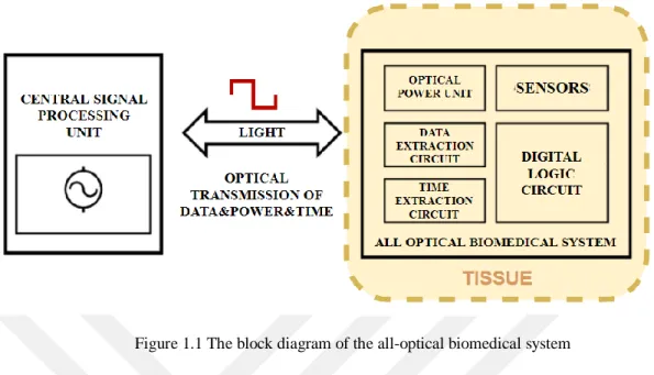
The block diagram of an all-optical biomedical system is shown in Figure 1.1. Power and data values are transmitted optically to this system. Power is transmitted with a laser of 40 mW or more for this type of microsystems to operate consistently. This is why, so that a kind of micro system which functions by this type of optical power works in an efficient way, it should consume low supply voltage and also low power [9]. In addition, the micro size of the presented system is critical for placement and portability. Therefore, it is foreseen that the all system must be implemented by using the same technology. CMOS technology is preferred for most of biomedical systems due its common usage, design conveniences and low cost.
Figure 1.1 The block diagram of the all-optical biomedical system
In this study, low power consuming sensor structures which operate with low voltage for all-optical biomedical system are investigated and these structures are compared. Three structures including LC CMOS cross coupled, relaxation and ring oscillator are investigated. These designs are compared by considering power consumption, supply voltage and output frequency values. Oscillator based sensing circuits are designed and simulated by using 180 nm UMC CMOS technology. Also, the theoretical equations of output frequency depending on the resistance and capacitance value are derived.
The all-optical microsystem incorporates an integrated CMOS phototransistor integrated into analog and digital circuits. Thanks to this receiver, data which comes from the transmitter is detected. The microsystem that operates with optical power and its programming operation carried out optically has been designed.
Moreover, communication protocols which are PWM and PAM are presented to transmit the data with single channel in this study. Thanks to designed circuit, the power consumption is reduced. Arduino Uno is used to represent the microsystem. Raspberry Pi 3B is used as a transmitter. Mutual data transmission is carried out by means of IR LED which is transmitter and phototransistor which is receiver. The different data is sent to the receiver via GUI which is designed on the Raspberry Pi.
3
2.
LOW POWER CMOS OSCILLATOR DESIGNS
Capacitive sensors are commonly used to detect values such as pressure changes and humidity values in biomedical and implant systems. The capacitance is changed when the pressure value on the capacitive sensor changes. The operation of capacitive sensor is based on conversion of measured physical parameter (pressure etc.) into capacitance. Many devices have been developed to convert it to measurable electronic signal.
Capacitance read out circuits are used to measure the capacitance changes. Especially, capacitance to frequency converter acts important role. In this way, capacitance change is translated to frequency value. CMOS oscillator is one of the techniques of capacitance to frequency converter.
Oscillator is an electronic circuit which produces a periodic and vibrating electronic signal. It consists of active and passive circuit element to produce repetitive signal at the output without external input signal. It produces a continuous and repeated waveform. Therefore, each different frequency value from oscillator is corresponds to different capacitance value.
In this study, the design and results of oscillator based capacitive and resistive sensing circuits with low supply voltage and low power consumption for an optically powered biomedical microsystem are presented. Three structures including LC CMOS cross coupled, relaxation and ring oscillator have been examined and compared in terms of their suitability for the optical system completely. The oscillator based sensing circuits are designed and simulated using 180 nm UMC CMOS Technology. In addition, the theoretical relationships of output frequency depending on sensor resistance and capacitance are derived. Moreover, it is also shown that the designed ring oscillator can work at 0.5 V supply voltage and it can be operated with a single integrated CMOS phototransistor without utilizing a voltage doubler circuit.
2.1. LC CMOS Cross Coupled Oscillator
LC CMOS cross coupled oscillator operates based on negative resistance. The MOSFET cross coupled pair generate a negative resistance.
(a) (b)
Figure 2.1 (a) MOSFET cross coupled pair, (b) Equivalent circuit of the cross coupled pair [10]
For the circuit which is in the Figure 2.1,
𝐺𝑥 = ix Vx = −gm 2R 2.1 so, 𝑅 = 1 Gx = −2 gm 2.2
The LC CMOS cross coupled oscillator behaves as an electrical resonator, storing energy oscillating at the circuit’s resonant frequency. The obtained angular oscillation frequency value is dependent on the inductance (L) and the capacitance (C) values with √𝐿𝐶 equation. The capacitance or inductance value can be found by measuring the output frequency. The circuit diagram of the designed LC CMOS cross coupled oscillator is shown in Figure 2.2.
5
Figure 2.2 The circuit diagram of the designed LC CMOS cross coupled oscillator
The LC CMOS cross coupled oscillator simulations are performed in Advanced Design System (ADS) simulation program. Simulation drawing of the designed oscillator is shown in Figure 2.3. The parameter values of the designed circuit are given in Table 2.1. The capacitor called C3 represents the capacitive sensor. The Ceq value with the transistor parasitic capacitance is calculated as 7.09 pF in Equation 2.3.
Table 2.1 The parameter values of the designed LC CMOS cross coupled oscillator
Parameter Value PMOS (W) 190 µm PMOS (L) 0.18 µm NMOS (W) 96 µm NMOS (L) 0.18 µm Inductor 4 nH Capacitor 4 pF
Figure 2.3 The circuit diagram of the designed LC CMOS cross coupled oscillator in ADS simulation program
Since the voltage value from the optical power unit can be in the 0.4 V-2 V range, various supply voltages which are in this range have been applied to the oscillator during the simulation. When 1.2 V voltage is applied to the LC CMOS cross coupled oscillator, the output frequency of the oscillator is 936 MHz, the average current is 1.643 mA and the power consumption is 1.972 mW. When 1 V voltage is applied to the LC CMOS cross coupled oscillator, the output frequency of the oscillator is 950.785 MHz, the average current is 649.9 µA and the power consumption is 649.9 µW. Simulation results of the designed LC CMOS cross coupled oscillator for 1 V is shown in Figure 2.4 and Figure 2.5. LC CMOS cross coupled oscillator has not oscillation under 1 V.
7
Figure 2.4 Simulation result of the designed LC CMOS cross coupled oscillator, VDD = 1 V
Figure 2.5 Power dissipation vs supply voltage graph of the designed LC CMOS cross coupled oscillator, VDD=1 V
An equation showing the relationship between frequency and capacitance is derived. The analytic equation of the oscillation frequency of the designed LC CMOS cross coupled oscillator is defined in Equation 2.3.
𝑓 = 1
When the capacitive sensor is used instead of the conjugate capacitance, the capacitance-frequency equation of the designed LC CMOS cross coupled oscillator can be expressed as in Equation 2.4.
𝑓 = 10751.97
𝐶0.433 2.4
The convergence parameters for the simulation results are calculated as R2 = 0.9946, aR2 = 0.9928, P = 1.57710-7, SE = 759.2, F = 552.3.
2.2. Relaxation Oscillator
Relaxation oscillator is a nonlinear oscillator circuit which produces a triangle wave or square wave. The circuit can consist of comparator, op amp or negative resistance device. The period of the relaxation oscillator depends on the time constant of the capacitor circuit. The active device regulates between charging and discharging modes. In other words, this oscillator alternates between two states at with a period that depends on the charging of a capacitor and so the oscillator creates discontinuously changing repetitive waveform. The capacitor voltage may change when charged or discharged from a constant voltage or current source.
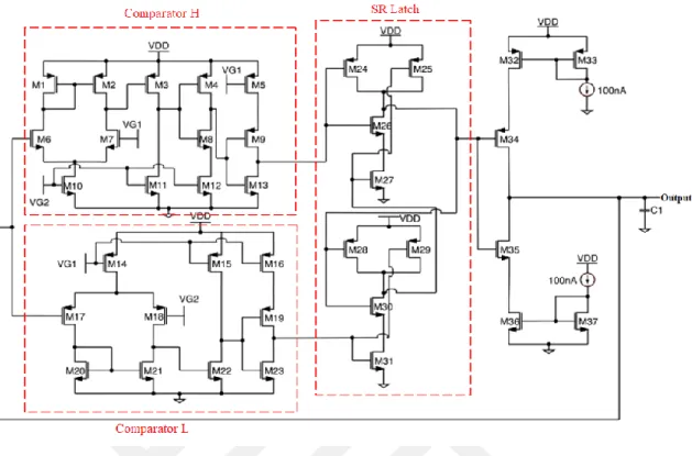
A relaxation oscillator can be built with a 555 timer integrated circuit. The 555 timer is an integrated circuit which be used in oscillator applications. When a chosen capacitor is charged to a value, comparators that are in the 555 timer flip a transistor switch that discharges that capacitor through a RC time constant to ground. When the capacitor falls to low value, the switch flips to let the capacitor charge up again.
The relaxation oscillator with the 555 timer is designed. This oscillator consists of two comparators, SR latch and a current source. The capacitor is charged with the 100 nA current source. When the voltage on the capacitor reaches the upper threshold, detected by the comparator H, RB goes low and resets the SR latch. Then, the capacitor is discharged. The discharging continues until the voltage on the capacitor reaches the lower threshold, detected by the comparator L. SB goes low and sets the SR latch. This begins again and so an oscillation occurs. The circuit diagram of the designed relaxation oscillator is shown in Figure 2.6.
9
Figure 2.6 The circuit diagram of the designed relaxation oscillator
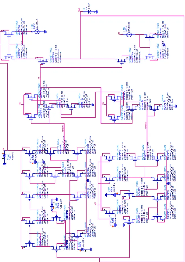
The relaxation oscillator simulations are performed in ADS simulation program. Simulation drawing of the designed oscillator is shown in Figure 2.7. The parameter values of the designed circuit are given in Table 2.2. The capacitor called C1 represents the capacitive sensor.
Table 2.2 The parameter values of the designed relaxation oscillator
Parameter Value PMOS (W) 1 µm PMOS (L) 0.24 µm NMOS (W) 1 µm NMOS (L) 0.24 µm Current Source 100 nA Capacitor 10 pF VG1 0.9 V VG2 0.2 V
11
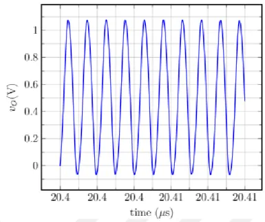
1.2 V and 1 V supply voltages are given to the relaxation oscillator for simulations. When 1.2 V voltage is applied to the relaxation oscillator, the output frequency of the oscillator is 93.220 kHz, the average current is 13.22 µA and the power consumption is 15.864 µW. When 1 V voltage is applied to the relaxation oscillator, the output frequency of the oscillator is 90.222 kHz, the average current is 6.172 µA and the power consumption is 6.172 µW. Simulation results of the designed relaxation oscillator for 1 V is shown in Figure 2.8 and Figure 2.9. Relaxation oscillator has not oscillation under 1 V.
Figure 2.8 Simulation result of the designed relaxation oscillator, VDD = 1 V
An equation showing the relationship between frequency and capacitance is derived. The analytic equation of the oscillation frequency of the designed relaxation oscillator is defined in Equation 2.5. Current coefficient is calculated as α = 10.23 x 10⁻².
𝑓 = αI
C (VG1 − VG2) 2.5
2.3. Ring Oscillator
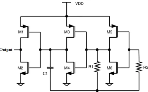
Ring oscillator is an electronic device which consists of an odd number of NOT gates in a close loop chain which provides an unstable negative feedback circuit. The NOT gates or inverters are arranged in a chain. The output of the last inverter is feedback into the first inverter. The output of the ring oscillator oscillates two voltage levels. These voltage levels are the voltage value and zero. The ring oscillator must have odd number of inverters because if this oscillator consists of even number of inverters, the last output is same as the input. The natural oscillation frequency of this structure varies with the additional resistance and capacitance values to be added. Thanks to this feature, ring oscillators can be used to determine capacitance and resistance values. The circuit diagram of the designed ring oscillator is shown in Figure 2.10.
13
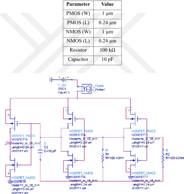
The ring oscillator simulations are performed in ADS simulation program. Simulation drawing of the designed oscillator is shown in Figure 2.11. The parameter values of the designed circuit are given in Table 2.3. In order to adjust the oscillation frequency, two resistors which are 100 kΩ values are added to the circuit. As the oscillation frequency is intended to be less than 1 MHz, a capacitor which is 10 pF value are added to represent the capacitive sensor.
Table 2.3 The parameter values of the designed ring oscillator
Parameter Value PMOS (W) 1 µm PMOS (L) 0.24 µm NMOS (W) 1 µm NMOS (L) 0.24 µm Resistor 100 kΩ Capacitor 10 pF
1.2 V, 1 V, 0.8 V and 0.5 V supply voltages are given to the ring oscillator for simulations. When 1.2 V voltage is applied to the ring oscillator, the output frequency of the oscillator is 452.514 kHz, the average current is 32.35 µA and the power consumption is 38.82 µW. When 1 V voltage is applied to the ring oscillator, the output frequency of the oscillator is 444.873 kHz, the average current is 20.75 µA and the power consumption is 20.75 µW. When 0.8 V voltage is applied to the ring oscillator, the output frequency of the oscillator is 437.698 kHz, the average current is 12.08 µA and the power consumption is 9.664 µW.
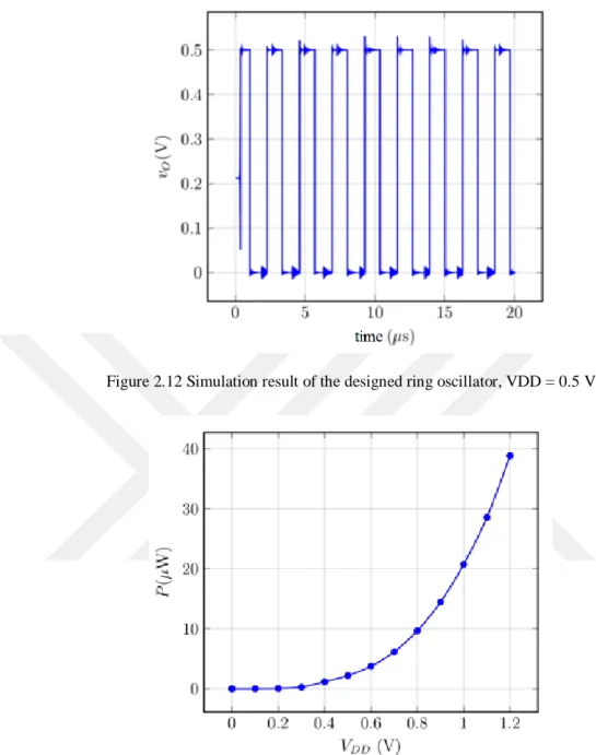
In the next step, Metal Oxide Semiconductor Field Effect Transistor (MOSFET) models with low threshold voltage are used to reduce the power consumption of the ring oscillator. 0.5 V are applied to the ring oscillator. The output frequency is measured as 428.295 kHz. The average current output is 4.382 µA while the power consumption is 2.191 µW. Simulation results of the designed ring oscillator using MOSFET models with low threshold voltage is shown in Figure 2.12 and Figure 2.13.
15
Figure 2.12 Simulation result of the designed ring oscillator, VDD = 0.5 V
Figure 2.13 Power dissipation vs supply voltage graph of the designed ring oscillator VDD=0.5 V
An equation showing the relationship between frequency and capacitance is derived. The analytic equation of the oscillation frequency of the designed ring oscillator is defined in Equation 2.6.
𝑓 = 1
The theoretical capacitance value-frequency change equation given in Equation 2.6 and the simulation results are shown on the same graph in Figure 2.14. It is understood that the equation obtained by theoretical equates with the simulation result. By using this equation, it is possible to calculate the capacitive sensor value and thus reach the humidity, temperature or pressure values expressed by the sensor.
Figure 2.14 Comparison of the theoretical and the simulation results for the designed ring oscillator in terms of oscillation frequency value
2.4. Comparison of The Designed Low Power CMOS Oscillator
The designed oscillators need between 0.5 and 0.7 V due to the circuit which is used. The LC CMOS cross coupled and the relaxation oscillator have not oscillation under 1 V. Hence, following results are obtained by providing 1 V with the LC CMOS cross coupled oscillator and the relaxation oscillator and also 0.5 V with the ring oscillator in the Table 2.4. These results are calculated as the best result for each oscillator.
17
Table 2.4 Comparison of the designed low power CMOS oscillator
LC CMOS Cross Coupled Oscillator Relaxation Oscillator Ring Oscillator The Output Frequency 950.785 MHz 90.222 kHz 428.295 kHz The Current Consumption
649.9 µA 6.172 µA 4.382 µA
The Power Consumption
649.9 µW 6.172 µW 2.191 µW
Minimum power consumption and minimum supply voltage conditions have been taken into consideration due to the system to be used in the designed oscillators. According to the results, the LC CMOS cross coupled oscillator has both high output frequency and high power consumption. The relaxation oscillator has no oscillations for desired voltage range were found in the system. When all these conditions are taken into consideration, the ring oscillator is suitable for this system. Also, the ring oscillator requires fewer transistor, so it is also advantageous in terms of the need for less circuit area requirements. Considering that the frequency value of the capacitance will be measured, setting the frequency value in the desired range is also expected from the sensor circuits. Since the LC CMOS cross coupled oscillator is oscillated depending on the L and C values, the frequency range can be determined by appropriate selection of these values. On the other hand, a high level of silicon is needed to increase the inductance value and it is practically impossible to obtain an integrated inductance value higher than nH [11]. Therefore, for sensor capacitance values in the pF range, the LC CMOS cross coupled oscillator output frequency values are in the 500 MHz-1 GHz range and also the power consumption is high. Since the oscillation frequency of the relaxation oscillator is related to the applied voltage values and the current source value, the oscillation frequency is easier to control. However, the studies show that the relaxation oscillator structure does not give a result at a level of 0.5 V - 0.7 V which is a single photodiode voltage. On the other hand, the ring oscillator works with a supply voltage of 0.5 V without the need for any voltage amplifying structure, so that the ring oscillator based sensing circuit can be operated with a single integrated photodiode.
According to the results in Table 2.4, it is considered appropriate to use ring oscillator as a sensing circuit in the designed CMOS chip. The sensing circuit has a ring oscillator structure with 3 inverters. On the other hand, it has a feedback system including capacitance and resistance values. According to these impedance values, the frequency of the ring oscillator has changed. The general structure of the sensing circuit is shown in Figure 2.15. The ring oscillator has met the requirement of low power consumption and small footprint for the microsystem.
19
3.
WIRELESS OPTICAL EMBEDDED SYSTEM REALIZATION
This chapter discusses wireless optical data transfer used within embedded systems.
Nowadays, many of the various embedded systems are required to use a kind of communication interface to data exchange with the environment or each other. In recent years, wireless technologies have become widespread due to their ease of use. Although wireless technologies dominate radio frequency devices, such as network or Bluetooth, some applications are taken advantage of an optical data connectivity.
A new serial communication protocol must be introduced for data transmission. Thus, the system should be arranged according to this protocol. There are some serial communication protocols such as RS-232, RS-485, I2C, SPI etc. and these techniques are widely used. In addition, power and data transmission in different channels have been realized in these protocols. In addition, these protocols result in high power consumption when the requirements of biomedical applications are considered. Therefore, instead of the existing protocols, a new serial communication protocol has been created which provides simplicity for low energy consumption.
Today, optical communication has been possible with the development of light emitting diodes having very low switching times and thus providing a way for high-speed data transmission. Optical communication uses LEDs to transmit pattern of data which is then received and decided by a receiver. The wavelengths of light sources used are generally around 900 nm.
The use of wireless communication in biomedical systems is provided. The aim is to provide this with wireless optical communication. Thus, low power consumption and small footprint designs required for biomedical systems can be provided. These designs can be microsystems produced with CMOS technology as described in the previous section. Since the microsystem is optically programmable, this feature of the project makes it different from the other applications.
In this project, a control panel is designed to control the biomedical system. Wireless optical embedded system realization is shown in Figure 3.1.
Raspberry Pi is used as control panel. Arduino Uno represents CMOS chip. Optical data transmission between the Raspberry Pi and the Arduino Uno is achieved thanks to optical communication protocol.
Figure 3.1 Wireless optical embedded system realization
3.1. Transmitter Design
The design is based on the Raspberry Pi single board computer.
The transmitter side is shown in Figure 3.2 and consists of the following parts: • Raspberry Pi 3B
• Raspberry Pi 3B DAC board • IR LED
21
Figure 3.2 (a) The block diagram of the system, (b) Designed transmitter circuit, (c) IR LED
The parts are described in detail in the following sections.
Thanks to the serial data which sends from the Raspberry Pi, the IR LED blinks. Both analog signal and digital signal are sent to the IR LED. The Raspberry Pi 3B has not DAC, so the DAC board is used to obtain analog signal at this point.
The analog signal which is shown in Figure 3.3 has 3 main characteristics: • Amplitude
• Frequency • Phase
Figure 3.3 Analog signal
Thanks to the analog signal sent with different voltage values and different wavelengths, different data is sent to the receiver via the IR LED. The IR LED emits different level of lights at these voltage levels and sends different data. Therefore, each voltage level has a different message. The difference in wavelength causes the frequency change of the signal. The relationship between wavelength and frequency is given in Equation 3.1.
𝜆 =c
f 3.1
An interface is designed to send different signals at different frequencies and this part is described in detail in the following sections.
The short and long pulse are interpreted as 0 and 1 by the receiver, when the data is sent as digital signal. This situation is shown in Figure 3.4. The duration of the pulse is calculated by the timers and the receiver detects different message sequences as 0 or 1. Therefore, each sequence is interpreted as the different message.
23
Figure 3.4 Digital signal
3.1.1. Raspberry Pi 3B
The Raspberry Pi which is credit card sized single board computer is designed by Raspberry Pi Foundation in England. The purpose of foundation is to teach programming to young children. It is a talented little device that enables people of all ages to explore computing and to learn how programming.
The Raspberry Pi is starting with a Secure Digital (SD) card containing operating system. Raspbian which is based on Debian is free and official operating system for all models of the Raspberry Pi. The Raspbian operating system is usually used by user, but there are third-party operating system images like Ubuntu MATE, Windows 10 Internet of Things (IoT) Core too.
The Raspberry Pi is widely used in embedded system domain. It is powerful device and it can be used to make various application like IoT applications, robotics, industrial/home automation and environmental sensing/monitoring. There are several types such as Raspberry Pi 1A+, 1B+, 2B, Zero, Zero W, 3B, 3B+ and 3A+. In this study, the Raspberry Pi 3B which is shown in Figure 3.5. is used.
Figure 3.5 Raspberry Pi 3B model [12]
The Raspberry Pi is transmitter part for this study. It acts a role as control panel in the wireless optical embedded system design as described in the Figure 3.1. Different messages are sent to receiver part via IR LED. The receiver part detects these messages and returns a different reply to each different message. The Raspberry Pi detects these messages via phototransistor.
3.1.2. Raspberry Pi 3B DAC board
Digital to analog converter (DAC) is a device which transforms digital signal into an analog signal. The DAC device converts digital signal like 0 and 1 into various current and voltage values.
The Raspberry Pi 3B has not DAC, so analog signal output is not taken from the Raspberry Pi 3B. Hence, DAC is necessary to convert digital signal to analog signal. Raspberry Pi high precision Analog to Digital / Digital to Analog (AD/DA) expansion board which is shown in Figure 3.6. is used for this reason. The analog signal is obtained by means of the DAC8532 on the board.
25
Figure 3.6 Raspberry Pi high precision AD/DA expansion board [13]
The DAC8532 has dual channel and 16-bit resolution. Thanks to these features, it is possible to get analog signal from 2 different channels for voltage values between 0 V and 5 V up to 216 digits. According to Equation 3.2, each digit corresponds to 0.0000763 V / digit.
Each Digit ( V Digit) =
5 V
65536= 0.0000763
Sinusoidal and triangle signal are obtained by using the AD/DA board and the DAC8532 library. Software is developed to obtain sinusoidal and triangle signal at different frequency. Also, GUI is designed to select type of signal and frequency value. Qt Creator Integrated Development Environment (IDE) is used for the software development and GUI design. Designed GUI is shown in Figure 3.7. Two buttons as sinusoidal and triangle are added to select type of signal. Thanks to dial, frequency value is selected. When the frequency value is changed via dial, it is written on the screen.
Figure 3.7 Designed GUI for DAC part
3.1.3. IR LED
Infrared is the region of the electromagnetic spectrum between microwaves and visible light. IR light and visible light have different the frequency and wavelength. IR has a longer wavelength. Infrared lies outside the range of visible light, so people can’t see it.
IR LED is a solid state lighting device that emits light in the infrared range which is between 700 nm and 1 mm wavelength of the electromagnetic radiation spectrum. Infrared communication is one of the widely used wireless communication technology because of common, cheap and easy to use. Also, IR needs low voltage. Because of the low power requirement of the micro system is taken into consideration, IR range is selected. The relationship between current and voltage for the LEDs is shown in Figure 3.8.
27
Figure 3.8 I – V curve of LEDs [14]
When voltage is applied, it emits lights and converts the electrical energy into light energy. The IR LED is a type of diode. Electrical characteristics of the IR LED is like PN junction diode. The diode allows to flow electric current in one direction. When the current flows, electrons fall from one part of the diode into holes on another part. In order to fall into these holes, the electrons must shed energy in the form of photons which produce light. Working structure of IR LED is shown in Figure 3.9.
The IR LED which is located on Raspberry Pi 3B and Arduino Uno plays transmitter role. Thanks to the short and long pulses sent, different messages are sent via the IR LED.
3.2. Receiver Design
The design is based on Arduino Uno microcontroller.
The receiver side is shown in Figure 3.10 and consists of the following parts: • Arduino Uno
• Phototransistor • 220 kΩ resistor
Figure 3.10 (a) The block diagram of the system, (b) Phototransistor, (c) Designed receiver circuit
The parts are described in detail in the following sections.
The serial data coming from the Raspberry Pi is detected by the phototransistor on the Arduino Uno. The light emitted from the IR LED falls on the phototransistor. The
29
phototransistor reads this light during a certain period of time. This light falling on the phototransistor is defined as 0 or 1. Hence, the message is detected. As described in the transmitter part, the data sequence sent as 0 and 1 is detected without any data loss.
3.2.1. Arduino Uno
The Arduino Uno is a microcontroller board based on the ATmega328. It is programmed with the Arduino software. The Arduino Uno is widely used in embedded system domain. It can be used to make various application like IoT applications, robotics, industrial/home automation and environmental sensing/monitoring. In this study, the Arduino Uno which is shown in Figure 3.11. is used.
Figure 3.11 Arduino Uno model [16]
The Arduino Uno is receiver part for this study. It acts a role as CMOS chip which has sensor, sensing circuit and digital logic circuit in the wireless optical embedded system design as described in Figure 3.1. The designed CMOS chip detects messages from the transmitter by the photodiode which is on it. These perceived messages are interpreted by the digital logic circuit on the CMOS chip. Thus, different data is sent according to different incoming messages. The designed CMOS chip is shown in Figure 3.12.
Figure 3.12 The layout of the CMOS integrated circuit
Different messages that comes from transmitter part are detected via phototransistor. The Arduino Uno sends different replies to each different message. The transmitter part detects these messages via phototransistor.
3.2.2. Phototransistor & Photodiode
Phototransistor is a type of transistor which converts the light energy into an electrical energy. Light sensitive substances such as Gallium Arsenide is used to increase the light sensitivity for phototransistors. The phototransistor can sense light levels and change the current flowing between emitter and collector according to the level of light it receives. The phototransistor has generally an exposed base that amplifies the light coming in contact with. Thanks to this base a relatively high current passes through the phototransistor. As the current spreads from the base to the emitter, the current is concentrated and converted into voltage. The structure of the phototransistor is shown in Figure 3.13.
31
Figure 3.13 Structure of phototransistor [17]
Photodiode is a type of PN junction diode which generates electric current when light its surface. The working of the photodiode depends on the intensity of light in contact with. The light incident on the diode reduces the width of their depletion region. Hence, the electrons and hole start moving across the region. While the electron moves towards the cathode, the hole moves toward the anode. Therefore, the current is induced in it. The working structure of the photodiode is shown in Figure 3.14.
Figure 3.14 Working structure of photodiode [18]
Both the phototransistor and the photodiode can be used to sense light. However, the phototransistor is more sensitive in view of the gain provided by the transistor. Unlike the
photodiodes, the phototransistor increases the current produced by light. Hence, the phototransistor is more suitable in applications.
In this study, the phototransistor is used. The phototransistor which is located on Raspberry Pi 3B and Arduino Uno plays receiver role. Different messages are detected via the phototransistor.
3.3. IR Transmission Between Raspberry Pi 3B and Arduino Uno
Infrared transmission refers to energy in the electromagnetic radiation spectrum region at wavelengths longer than visible light. It is used to send data at high speed. The IR transmission is a wireless communication which has IR transmitter and receiver.
The Raspberry Pi which is transmitter and the Arduino Uno which is receiver is described in separate sections. The data is sent via the IR LED and detected by the phototransistor on the opposite side. Moreover, the IR LED and the phototransistor have been added to both parts for data exchange. Optical communication protocol is developed to transmit and receive the data. Thanks to the optical communication protocol, the data is transmitted at high speed and the system consumes very low power.
Firstly, the data is sent optically from the Raspberry Pi via the IR LED and is detected by the phototransistor on the Arduino Uno. The Arduino receives the data. Based on detected data, the phototransistor triggers the IR LED on the Arduino. The data is sent to the Raspberry Pi via the IR LED again. Finally, the data is detected by the phototransistor and monitored on the Raspberry Pi. Hence, the message is received. The algorithm of IR transmission is shown in Figure 3.15.
33
Figure 3.15 The algorithm of IR transmission
The sending data is shown in Figure 3.16. Data has been sent and received successfully. The results of data transmission are described in detail in the following section.
3.4. Experimental Results
As shown in Figure 3.17, an experimental setup is established. In this arrangement, Arduino Uno is used as receiver and Raspberry Pi is used as transmitter. Optical communication is used to communicate each other. A protocol has been developed to provide this communication. Both Raspberry Pi and Arduino Uno have IR led, phototransistor and resistance.
Figure 3.17 (a) The experimental setup of IR transmission, (b) Receiver, (c) Transmitter
Thanks to the serial data which sends from the Raspberry Pi, the IR LED blinks. The phototransistor reads the serial data. Both analog signal and digital signal are sent to the IR LED.
Thanks to the analog signal sent with different voltage values and different wavelengths, different data is sent to the receiver via the IR LED. The IR LED emits different level of lights at these voltage levels and sends different data. Therefore, each voltage level has a different message. The difference in wavelength causes the frequency change of the signal.
Sinusoidal and triangle signal are obtained by means of developing application. As mentioned previous section, GUI is developed for this application. Two buttons as sinusoidal
35
and triangle are added to select type of signal. Thanks to dial, frequency value is selected. When the frequency value is changed via dial, it is written on the screen.
Figure 3.18 Obtained triangle signal
Table 3.1 Comparison of code and measurement value for triangle signal
Code Value Measurement Value
tempFrequency (s) = 10000 5000 1000 T = 1s, f = 1 Hz T = 510 ms, f = 1.96 Hz T = 111.04 ms, f = 9 Hz
In Figure 3.18, the obtained triangular signal and values is shown. Different values are given and analyzed. The obtained data obtained as a result of the studies carried out by giving different values are given in Table 3.1. There is a difference of approximately 10000 times between the frequency given in the code and the measurement taken from the oscilloscope because of the crystal oscillator found in the Raspberry Pi.
Figure 3.19 Obtained sinusoidal signal
Table 3.2 Comparison of code and measurement value for sinusoidal signal
Code Value Measurement Value
tempFrequency (s) = 5000 1000
T = 714.29 ms, f = 1.4 Hz T = 145.45 ms, f = 6.87 Hz
In Figure 3.19, the obtained sinusoidal signal and values is shown. Different values are given and analyzed. The obtained data obtained as a result of the studies carried out by giving different values are given in Table 3.2. There is a difference of approximately 7 times between the frequency given in the code and the measurement taken from the oscilloscope because of the crystal oscillator found in the Raspberry Pi.
The short and long pulse are interpreted as 0 and 1 by the receiver, when the data is sent as digital signal. The duration of the pulse is calculated by the timers and the receiver detects different message sequences as 0 or 1. Therefore, each sequence is interpreted as the different message.
The first stage of communication is the transmission of data from the raspberry via the IR LED. The oscilloscope view of the sending data is given in Figure 3.20. As shown in Figure 3.20, long pulses are taken as 1, short pulses are taken as 0. The y-axis represents the voltage value and the x-axis represents the time.
37
Figure 3.20 Oscilloscope view of the sending data
As described in the previous section, the sending data is "010110111011110". The sending data is detected by the phototransistor on the Arduino Uno. The received data is shown in Figure 3.21. With the value 0 between the data, the information of received data is obtained.
Figure 3.21 The data detected by the receiver
Finally, when the Arduino receives the data, the phototransistor triggers the IR LED on the Arduino based on detected data. If the data is long pulse, the IR LED lights. If the data is short pulse, the IR LED does not light so that the data is sent back to the receiver. The sending data is detected by the phototransistor and monitored on the Raspberry Pi. The data detected by the Raspberry Pi is shown in Figure 3.22. Hence, the optical communication has been completed.
Figure 3.22 The data detected by the transmitter
According to the results of the experiment, the data is sent and received successfully. There is no data loss during this communication. This type of wireless infrared communication systems is useful for systems requiring low cost and low power consumption.
39
4.
RESULTS & CONCLUSION
The research reported in this thesis consists of the design and comparison of oscillator based sensing circuits which have low power consumption and communication protocols which are PWM and PAM to transmit the data for an optically powered biomedical microsystem. The different data is sent to the receiver via GUI which is designed on the Raspberry Pi.
Three structures including LC CMOS cross coupled, relaxation and ring oscillator are investigated. In consequence of research and simulations, the ring oscillator is appropriate for the designed system because the ring oscillator consumes ultra low power than other designed oscillators. The designed optically powered biomedical microsystem needs between 0.5 and 0.7 V. The ring oscillator can work with a 0.5 V supply voltage. Also, the ring oscillator requires fewer transistor, so it needs less circuit area. Because of these reasons, the layout of the ring oscillator is design for optically powered biomedical microsystem.
The theoretical equations of output frequency depending on the resistance and capacitance value are derived. In this way, a frequency value can be calculated according to the capacitance value coming from the capacitive sensor in the microsystem.
Finally, embedded system is designed. The optical communication protocols which PWM and PAM are developed to transmit the data. Thanks to designed circuit, the power consumption is reduced. Arduino Uno is used to represent the microsystem. Raspberry Pi 3B is used as a transmitter. Mutual data transmission is carried out by means of the IR LED which is transmitter and phototransistor which is receiver. Different data is sent to the receiver and serves as a control panel with the GUI designed on the Raspberry Pi.
5.
REFERENCES
[1] K. Agarwal, R. Jegadeesan, Y. Guo and N. Thakor, "Wireless Power Transfer
Strategies for Implantable Bioelectronics," EEE Reviews in Biomedical Engineering, vol. 10, pp. 136-161, 2017.
[2] F. Ali, W. Raza, X. Li, H. Gul and K. Kim, "Piezoelectric Energy Harvesters for Biomedical Applications," Nano Energy, vol. 57, pp. 879-902, 2019.
[3] P. Bose, A. Khaleghi, M. Albatat, J. Bergsland and I. Balasingham, "RF Channel Modeling for Implant-to-Implant Communication and Implant to Subcutaneous Implant Communication for Future Leadless Cardiac Pacemakers," IEEE Transactions on Biomedical Engineering, vol. 65, no. 12, pp. 2798-2807, 2018. [4] H. Lee, B. Choi, K. S, S. Kim, W. Bae and S. Kim, "Sensitivity-Enhanced LC
Pressure Sensor for Wireless Bladder Pressure Monitoring," IEEE Sensors Journal, vol. 16, no. 12, pp. 4715-4724, 2016.
[5] R. Aragonés, P. Álvarez, J. Oliver and C. Ferrer, "Comparison of Readout Circuitry Techniques for Data Acquisition in Raw Sensor Systems," 2010.
[6] J. Drazan, O. Abdoun, M. Wassick, R. Dahle, L. Beardslee, G. Marcus, N. Cady and E. Ledet, "Simple Implantable Wireless Sensor Platform to Measure Pressure and Force," Medical Engineering & Physics, vol. 59, pp. 81-87, 2018.
[7] A. L. T. M. Q. N. H. B. Quadir NA, "Low-Power Implanted Sensor for Orthodontic Bond Failure Diagnosis and Detection," IEEE Sensors Journal, vol. 18, no. 7, pp. 3003-3009, 2018.
[8] C. Chiang, C. Lin ve M. Ju, «An Implantable Capacitive Pressure Sensor for Biomedical Applications”,» Sensors and Actuators A: Physical, cilt 134, no. 2, pp. 382-388, 2007.
[9] B. Sarioglu, M. Tumer, U. Cindemir, B. Camli, G. Dundar, C. Ozturk and A. Yalcinkaya, "An Optically Powered CMOS Tracking System for 3 T Magnetic Resonance Environment," IEEE Transactions on Biomedical Circuits and Systems, vol. 9, no. 1, pp. 12-20, 2015.
[10] A. Arbabian and J. Rabaey. [Online]. Available:
http://bwrcs.eecs.berkeley.edu/Classes/icdesign/ee142_f10/Lectures/Lect25_2up.pdf. [11] E. Ashenafi ve M. Chowdhury, «Noise Voltage Analysis of Spiral Inductor for
On-Chip Buck Converter Design,» IEEE International Symposium on Circuits and Systems (ISCAS), pp. 1-4, 2017.
[12] [Online]. Available: https://www.robotistan.com/raspberry-pi-3.
[13] [Online]. Available: https://www.waveshare.com/High-Precision-AD-DA-Board.htm.
[14] "Dealing with LEDs using an STM32," 2018. [Online]. Available: https://www.playembedded.org/blog/leds-stm32/.
[15] "Light Emitting Diodes Circuit Working Principle and Application," [Online]. Available: https://www.elprocus.com/light-emitting-diode-led-working-application/. [16] [Online]. Available: http://tecnokolik.com/arduino-nedir/.
[17] "Photodiode," [Online]. Available: https://www.physics-and-radio- electronics.com/electronic-devices-and-circuits/semiconductor-diodes/photodiodesymboltypes.html.
41
[18] "Phototransistor Basics, Circuit Diagram, Advantages & Applications," [Online]. Available: https://www.elprocus.com/phototransistor-basics-circuit-diagram-advantages-applications/.
REFERENCES NOT CITED
Yelkenci, A., Optically Powered and Optically Programmable CMOS Based Biomedical Microsystem İstanbul Bilgi University, 2017.
Bashirullah R. “Wireless Implants”. IEEE Microwave Magazine, 11 (7), 14-23, 2010.
Gutruf P, Rogers JA. “Implantable, Wireless Device Platforms for Neuroscience Research”. Current Opinion in Neurobiology, 50, 42-49, 2018.
Jiang L, Yang Y, Chen R, Lu G, Li R, Li D, Humayun MS, Shung KK, Zhu J, Chen Y, Zhou Q. “Flexible Piezoelectric Ultrasonic Energy Harvester Array for Bio-Implantable Wireless Generator”. Nano Energy, 56, 216-224, 2019.
Pavelková R, Vala D, Gecová K. “Energy Harvesting Systems Using Human Body Motion”. IFAC-PapersOnLine, 51 (6), 36-41, 2018.
Wang S, Koickal TJ, Hamilton A, Mastropaolo E, Cheung R, Abel A, Smith LS, Wang L. “A Power-Efficient Capacitive Read-Out Circuit with Parasitic-Cancellation for MEMS Cochlea Sensors”. IEEE Transactions on Biomedical Circuits and Systems, 10 (1), 25-37, 2016.
Brandon C, Elliott D, Moez K. “An Ultra Low-Voltage Low-Power Capacitance-to-Digital Converter for Wirelessly Powered Intraocular Pressure Sensor”. IEEE Journal of Radio Frequency Identification, 1 (3), 208-218, 2017.
Wang Y, Goh WL, Lee JH, Chai KTC, Je M. “Resonant-Based Capacitive Pressure Sensor Read-Out Oscillating at 1.67 GHz in 0.18μm CMOS”. World Academy of Science, Engineering and Technology International Journal of Electrical, Computer, Energetic, Electronic and Communication Engineering, 7 (7), 375-378, 2013.
Shih YC, Shen T, Otis BP. “A 2.3μW Wireless Intraocular Pressure/Temperature Monitor”. 2010 IEEE Journal of Solid-State Circuits Conference, 46 (11), 2592-2601, 2011.
43
Karipott SS, Veetil PM, Nelson BD, Guldberg RE, Ong KG. “An Embedded Wireless Temperature Sensor for Orthopedic Implants”. IEEE Sensors Journal, 18 (3), 1265-1272, 2018.
Cirmirakis D, Demosthenous A, Saeidi N, Donaldson N. “Humidity-to-Frequency Sensor in CMOS Technology with Wireless Readout”. IEEE Sensors Journal, 13 (3), 900-908, 2013.
Camli B, Sarioglu B, Yalcinkaya AD. “Photodiodes for Monolithic CMOS Circuit Applications”. IEEE Journal of Selected Topics in Quantum Electronics, 20 (6), 336-343, 2014.
“Teach, Learn, and Make with Raspberry Pi – Raspberry Pi” [online], www.raspberrypi.org/. [retrieved Sep 1, 2019]
Cetin, A.B.. “Raspberry Pi Nedir?” Mekatronik Mühendisliği Platformu & Blog I Forum, [online], 27 Sept. 2018, www.mekatronikmuhendisligi.com/raspberry-pi-nedir.html.
“DAC Ve ADC.” Diyot.net, [online], 7 Dec. 2015, diyot.net/dac-ve-adc/.
“ArduinoTürkiye.” Blogify, [online], arduinoturkiye.com/arduino-uno/ [retrieved Sep 1,2019]
“Introduction.” Arduino, [online] www.arduino.cc/en/guide/introduction, [retrieved Sep 1,2019]
“Buy Infrared LED with Cheap Price” [online]
Https://Www.robotistan.com/,www.robotistan.com/infrared-ledkizil-otesi-led, [retrieved Sep 1,2019]
“IR LED: Infrared Sensors: Pin Diagram & Working.” Electronics For You, [online], 12 Mar. 2019, electronicsforu.com/resources/learn-electronics/ir-led-infrared-sensor-basics.
“Light-Emitting Diodes Circuit, Working Principle and Application.” ElProCus, [online], 16 May 2018, www.elprocus.com/light-emitting-diode-led-working-application/.
Designed by www.1234.info / Modified: Your Name. RazorConcepts, [online], www.razorconcepts.net/phototransistor.html, [retrieved Sep 1,2019]
Olgun, E.. “Foto Transistör Nedir?” Teknoloji Projeleri, [online], 9 Feb. 2019, teknolojiprojeleri.com/elektronik/foto-transistor-nedir.
“What Is a Phototransistor?” Tech, [online], www.tech-faq.com/what-is-a-phototransistor.html. [retrieved Sep 1,2019]
Notes, Electronics. “What Is a Phototransistor: Tutorial & Primer.” Electronics Notes, [online],www.electronics-notes.com/articles/electronic_components/transistor/what-is-a-phototransistor-tutorial.php.[ retrieved Sep 1,2019]
“Difference Between Photodiode & Phototransistor (with Comparison Chart ).” Circuit Globe, 23 Dec. 2017, [online] circuitglobe.com/difference-between-photodiode-and-phototransistor.html.
“720-SFH309FA-5 Osram Opto Semiconductor Phototransistors.” Mouser Electronics
Turkey - Electronic Components Distributor, [online]
www.mouser.com.tr/Search/Refine?Keyword=720-SFH309FA-5. [ retrieved Sep 1,2019]
BASIC PHOTOPHYSICS, [online], photobiology.info/Visser-Rolinski.html. [ retrieved Sep 1,2019]
Editor, Author: Technical. “Light Emitting Diode(LED).” Polytechnic Hub, [online] 30 Mar. 2017, www.polytechnichub.com/l-e-d/.
McCormack, G. “1d: Principles of Data Communications: Analogue Modulation
Techniques” [online], Analogue
Signals,www.sqa.org.uk/learning/NetTechDC01DCD/page_04.htm.
IR Communication, [online], learn.sparkfun.com/tutorials/ir-communication/all. [ retrieved Sep 1,2019]
45
“How to Set Up an IR Remote and Receiver on an Arduino.” Circuit Basics, [online], 13 Aug. 2018, www.circuitbasics.com/arduino-ir-remote-receiver-tutorial/.
APPENDIX A: RASPBERRY PI 3B DAC CODE
dac8532_test.h #ifndef DAC8532_TEST_H #define DAC8532_TEST_H #include <bcm2835.h> #include <stdio.h> #include <unistd.h> #include <string.h> #include <math.h> #include <errno.h>#define SPICS RPI_GPIO_P1_16 //P4 #define CS_1() bcm2835_gpio_write(SPICS,HIGH) #define CS_0() bcm2835_gpio_write(SPICS,LOW) #define uint8_t unsigned char
#define uint16_t unsigned short #define channel_A 0x30
#define channel_B 0x34 void callSinFlag(); void callTriangleFlag(); void getFreq(int a);
void bsp_DelayUS(uint64_t micros);
void Write_DAC8532(uint8_t channel, uint16_t Data); uint16_t Voltage_Convert(float Vref, float voltage); int test_DAC(); #endif mainwindow.h #ifndef MAINWINDOW_H #define MAINWINDOW_H #include <QMainWindow> namespace Ui {
47
class MainWindow; }
class MainWindow : public QMainWindow {
Q_OBJECT public:
explicit MainWindow(QWidget *parent = 0); ~MainWindow();
private slots:
void on_dial_valueChanged(int value); void on_pushButton_clicked(); void on_pushButton_2_clicked(); private: Ui::MainWindow *ui; }; #endif // MAINWINDOW_H mythread.h #ifndef MYTHREAD_H #define MYTHREAD_H #include <QObject> #include <QThread>
class MyThread:public QThread { Q_OBJECT public: explicit MyThread(); void run(); signals: public slots: }; #endif
dac8532_test.cpp #include "dac8532_test.h" #include <qdebug.h> #include <qthread.h> #include "mainwindow.h" int tempFrequency = 0; int sinFlag = 0; int triangleFlag = 0; void callSinFlag() { sinFlag = 1; triangleFlag = 0; } void callTriangleFlag() { triangleFlag = 1; sinFlag = 0; } void getFreq(int a) { tempFrequency = a; }
void bsp_DelayUS(uint64_t micros) {
bcm2835_delayMicroseconds (micros); }
void Write_DAC8532(uint8_t channel, uint16_t Data) { uint8_t i; CS_1() ; CS_0() ; bcm2835_spi_transfer(channel); bcm2835_spi_transfer((Data>>8));
49
bcm2835_spi_transfer((Data&0xff)); CS_1() ;
}
uint16_t Voltage_Convert(float Vref, float voltage) {
uint16_t _D_;
_D_ = (uint16_t)(65536 * voltage / Vref); return _D_; } int test_DAC() { uint16_t i; uint16_t tmp; if (!bcm2835_init()) return 1; bcm2835_spi_begin(); bcm2835_spi_setBitOrder(BCM2835_SPI_BIT_ORDER_LSBFIRST ); bcm2835_spi_setDataMode(BCM2835_SPI_MODE1); bcm2835_spi_setClockDivider(BCM2835_SPI_CLOCK_DIVIDER_1024); bcm2835_gpio_fsel(SPICS, BCM2835_GPIO_FSEL_OUTP); bcm2835_gpio_write(SPICS, HIGH); i = 0; tmp=0; float pi = 3.14; while(1) {
if(sinFlag && !triangleFlag) {
qDebug()<< "freq value: " << tempFrequency;
Write_DAC8532(0x30, Voltage_Convert(5.0, 2.5 + sin(2 * pi * i / tempFrequency))); i++;
if(i==tempFrequency) {
i=0; } } if(triangleFlag == 1) { uint16_t i; uint16_t tmp; if (!bcm2835_init()) return 1; bcm2835_spi_begin(); bcm2835_spi_setBitOrder(BCM2835_SPI_BIT_ORDER_LSBFIRST ); bcm2835_spi_setDataMode(BCM2835_SPI_MODE1); bcm2835_spi_setClockDivider(BCM2835_SPI_CLOCK_DIVIDER_1024); bcm2835_gpio_fsel(SPICS, BCM2835_GPIO_FSEL_OUTP); bcm2835_gpio_write(SPICS, HIGH); i = 0; tmp=0;
while(triangleFlag && !sinFlag) { if(tmp==0) { Write_DAC8532(0x30, Voltage_Convert(5.0,0.00+(float)i/10)); i++; if(i==50) { i=0; tmp=1; } bsp_DelayUS(tempFrequency); } else if(tmp==1) { Write_DAC8532(0x30,Voltage_Convert(5.0,5.000-(float)i/10));
51 i++; if(i==50) { i=0; tmp=0; } bsp_DelayUS(tempFrequency); } }
qDebug()<< "time value: " << tempFrequency; } } bcm2835_spi_end(); bcm2835_close(); return 0; } main.cpp #include "mainwindow.h" #include <QApplication> #include "dac8532_test.h" #include <QHBoxLayout> #include <QSlider> #include <QSpinBox>
int main(int argc, char *argv[]) {
QApplication a(argc, argv); MainWindow w;
w.show(); return a.exec(); }
mainwindow.cpp #include "ui_mainwindow.h" #include "dac8532_test.h" #include "mythread.h" #include <QDebug> int frequency = 0; MainWindow::MainWindow(QWidget *parent) : QMainWindow(parent), ui(new Ui::MainWindow) { ui->setupUi(this);
MyThread *thread = new MyThread(); thread->start(); } MainWindow::~MainWindow() { delete ui; }
void MainWindow::on_dial_valueChanged(int value) {
qDebug() << "on dial: " << value; getFreq(value);
frequency = value;
ui->lcdNumber->display(frequency); qDebug() << "change freq: " << frequency; }
void MainWindow::on_pushButton_clicked() //sin {
callSinFlag();
on_dial_valueChanged(frequency); }
void MainWindow::on_pushButton_2_clicked() //triangle {
53 callTriangleFlag(); on_dial_valueChanged(frequency); } mythread.cpp #include "mythread.h" #include <QDebug> #include "dac8532_test.h" #include "mainwindow.h" MyThread::MyThread() { } void MyThread::run() { while(1) test_DAC(); }
APPENDIX B: TRANSMITTER CODE
mainwindow.h #ifndef MAINWINDOW_H #define MAINWINDOW_H #include <QMainWindow> namespace Ui { class MainWindow; }class MainWindow : public QMainWindow {
Q_OBJECT public:
explicit MainWindow(QWidget *parent = 0); ~MainWindow(); void sendData(); void receiveData(); private: Ui::MainWindow *ui; }; #endif // MAINWINDOW_H main.cpp #include "mainwindow.h" #include <QApplication> int main(int argc, char *argv[]) {
QApplication a(argc, argv); MainWindow w;
w.show(); return a.exec(); }
55 mainwindow.cpp #include "mainwindow.h" #include "ui_mainwindow.h" #include <wiringPi.h> #include <softPwm.h> #include <stdlib.h> #include <QDebug> #define IRLed 25 #define photoTransistor 22 #define PWMRange 100 int read; short sendingData[15] = {0, 1, 0, 1, 1, 0, 1, 1, 1, 0, 1, 1, 1, 1, 0}; int i; MainWindow::MainWindow(QWidget *parent) : QMainWindow(parent), ui(new Ui::MainWindow) { ui->setupUi(this); wiringPiSetup(); pinMode(IRLed, OUTPUT); pinMode(photoTransistor, INPUT); while (1) { sendData(); receiveData(); } } MainWindow::~MainWindow() { delete ui; }
void MainWindow::sendData() { for (i = 0; i <= 15; i++) { if(sendingData[i] == 1) { digitalWrite(IRLed,HIGH); delay(8); digitalWrite(IRLed,LOW); delay(2); } else { digitalWrite(IRLed,HIGH); delay(2); digitalWrite(IRLed,LOW); delay(8); } } } void MainWindow::receiveData() { read = digitalRead(photoTransistor); qDebug() << "value " << read; }
57
APPENDIX C: RECEIVER CODE
#include <SoftwareSerial.h> #define photoTransistor A1 #define IRLed 6
int reading = 0;
unsigned long duration; void setup() { pinMode(photoTransistor,INPUT); pinMode(IRLed,OUTPUT); Serial.begin(9600); } void loop() {
duration = pulseIn(photoTransistor, LOW); if (duration > 500) { if (duration <= 3000) { Serial.print("0"); digitalWrite(IRLed,LOW); } else { Serial.print("1"); digitalWrite(IRLed,HIGH); } } }