© TÜBİTAK
doi:10.3906/elk-1809-46 h t t p : / / j o u r n a l s . t u b i t a k . g o v . t r / e l e k t r i k /
Research Article
THD minimization for Z-source-based inverters with a novel sinusoidal PWM
switching method
Davood GHADERI∗,
Department of Electrical and Electronics Engineering, Faculty of Engineering, Bursa Technical University, Bursa, Turkey
Received: 07.09.2018 • Accepted/Published Online: 17.03.2019 • Final Version: 26.07.2019
Abstract: This paper presents a modified sinusoidal pulse width modulation (SPWM) switching method for one-phase and investigated two-phase impedance-source inverter structures. The proposed structure generates pulses for a quasi-Z-source converter and this block produces a unilateral voltage sine wave in the block’s output. This signal is applied to the inverter as its input wave. For this purpose, the novel SPWM method is proposed for power switches while being switched complementarily. Two power switches are used in the structure to generate the pure sinusoidal output voltage and to minimize total harmonic distortion (THD), which is an essential parameter in inverter design. The results show that the proposed method generates the pure sinusoidal voltage and current signals for resistive and inductive loads and pure voltage and improved current waves for capacitive loads in comparison with existing techniques, since the THD of the output voltage and current signals is strongly affected by the dynamic loads. This method leads to final cost improvement and reduction of the size of the system with fewer number of components, which are essential parameters for renewable energy resource applications. A mathematical model is validated with the 2017a version of MATLAB/Simulink and 1.51% and 1.33% THD values are reported for low and high power loads, respectively, in the one-phase structure and 0.95% and 0.87% in the two-phase system. Finally, a 120 W prototype has been implemented and tested. A sine-wave with 620 Vac peak to peak amplitude and 50 Hz frequency has been gained in the inverter’s output and the quality of the voltage and current waveforms has been evaluated for different two 1.8 k Ω and 600 Ω resistive loads in the one-phase structure. Experimental results confirm all mathematical and simulation results. Key words: Impedance source inverter, H bridge inverter, total harmonic distortion, Fourier analysis
1. Introduction
Considering the reduction in the amount of fossil fuel reserves and their damage to nature, renewable energy sources (RESs) as alternative energy resources are emerging to ensure sustainable energy production. For example, photovoltaic panels generate a DC voltage and need to be equipped with a boost or buck-boost converter to enhance the level of DC voltage and an inverter block to convert the DC signal to an AC one for household or industrial applications. Traditional voltage source inverters (VSIs) and current source inverters (CSIs) have several common problems such as the inability to use buck-boost converters in the structure and the necessity of applying one buck or boost converter. The VSI main circuit cannot be used for the CSI, and vice versa, and other main circuits are not interchangeable and their reliability is affected by EMI noise. Various studies have been done in analyzing inverter structures in order to connect to microgrid applications [1–3]. Inverters can be divided into two categories: isolated and nonisolated structures. Isolated inverters not ∗Correspondence: davood.ghaderi@btu.edu.tr
only are expensive and heavy and have larger size in comparison with nonisolated inverters, but also, because of the existence of transformers in their circuits, normally they are not efficient [4–6]. Considering the weight, size, and cost, isolated inverters include a high-frequency transformer that is called a fly-back inverter [7–10], a serial connection of a DC-DC converter and a full bridge inverter [11, 12], and a serial connection of a DC-DC converter, a transformer, and an AC-AC converter [12]. The fly-back type of inverter has several advantages like wide input voltage range and lower voltage rating on secondary components, but it has a higher EMI value because of the gap in the transformer and higher current ripples, and it needs a larger amount of input and output capacitors. The efficiency of a fly-back inverter is between 75% and 80% and it is not very suitable for RES applications [7, 8]. The application of transformerless inverters requires accurate calculation for the connection between the input DC voltage source and the grid side, which is a well-known safety issue. For example, if the photovoltaic panel the and grid side’s ground is not the same, a variable common mode voltage signal will be produced and will create a leakage current that will pass through the parasitic capacitor between the PV panel and the ground, and so the grid side’s current quality will be affected and it will increase the EMI of the structure directly [13]. For overcoming this leakage current, usually half or full bridge converters are applied. These converters use bipolar sinusoidal pulse width modulation or SPWM techniques. Not generating the common mode voltage is another advantage of these inverters. The main problem of the half bridge converter is that it needs a high DC voltage in input pins to generate a 220 Vac signal at the output; for that, application of a serial connection between PV panels or use of DC-DC boost converters is inevitable. Full bridge inverters need smaller DC voltages and approximately half of the DC voltage that should be used for the half bridge converter [14, 15]. Schmidt et al. [16] presented a highly efficient and reliable inverter concept (HERIC) structure containing from a full-bridge inverter and an AC bypass or FB-ACBP. Although in this topology a minimized and acceptable leakage current can be obtained, the common mode oscillation for the voltage can be addressed by considering the not-clamped potential for the freewheeling path. In [17] a topology was presented to eliminate the common mode current, but it needs an additional power switch. A group of transformerless inverters with flying capacitor was presented in [18] in order to evaluate and minimize this leakage current. In several references, doubled grounded topologies are suggested to minimize the leakage current problem. These converters have higher safety standards and are cheap and simple to investigate [19]. These topologies can produce a high voltage gain and have safety advantages, but all have complicated control structures. Recently, especially for photovoltaic applications, the Z-source inverter type has been considered and analyzed. The main advantage of this inverter is that leakage current and ground features are not considered in this topology. For transformerless applications, for obtaining a qualified power factor, several important issues like total harmonic distortion, DC current injection, and output voltage and current regulation should be considered. In order to limit the total harmonic distortion (THD) in output current or voltage signals, various PWM methods are intensively studied in pure sinusoidal inverters [20, 21]. For a pulse width modulation (PWM) technique, the voltage gain is determining by calculating the ratio of the fundamental components of the AC side’s voltage to the DC voltage of the input side. Classic sinusoidal PWM techniques normally use a reference sinusoidal wave and a carrier rectangular wave. A comparison was done between specific harmonic elimination (SHE-PWM) and single carrier sinusoidal PWM (PWM-SC) in [14]. The main drawback of specific harmonic elimination pulse width modulation techniques is obtaining an analytical resolution of the system of nonlinear equations that finally includes the trigonometric terms that ensure multiple sets of resolutions. A voltage injection method into the reference signal was investigated in [15]. This vector includes two tuning vectors, one for assuring the measurement time and another for maintaining the average value of the reference
voltage vector as the countervailing vector. In the first and later periods of PWM and at the frequency of the carrier, two least injection voltage vectors are interpolated to the reference vector and the sequence of these vectors is directly connected to the magnitude of the harmonic terms of the voltage. This technique is complex for the implementation affairs. A precalculated PWM method was presented in [21]. In implementations, the existent harmonics of the DC source can introduce more noncharacteristic harmonics because of the finite DC bus capacitance and other realistic applicable conditions. A multicell cascade inverter structure was introduced in [22] and a repetitive control structure was illustrated in [23–25]. In all of these structures, the THD value is around 2.23%–8.8% for voltage and especially current signals. Furthermore, cascade topologies utilize more power switches so they have more complexity, larger size, higher price, and lower efficiency. This study presents a novel SPWM switching method for Z-source converters connected to H bridge inverters. Based on simulation results, when the second load is switched on, there is no difference in the output voltage signal and the change in the current wave is observed at an acceptable level. This study has significant improvement in the simultaneous switching of the power MOSFETs by SPWM topology. Z-source converters [26] are presented for RES-based applications because of their performance, efficiency, and low cost. This inverter not only does not need doubly grounded problems features and calculations, but also it has suitable power quality without applying any type of THD limiter structures. One of the other benefits of the semi-Z-source inverter structure is that to produce a sinusoidal voltage signal through a load we need to apply only two power switches and this can directly decrease the complexity and total cost of the proposed structure. The facility of the proposed structure has been considered not only for resistive and inductive loads, but also for the capacitive and combination loads. Our other reason to work on the quasi-Z-source inverter structure is that the Z-source topology requires LC network placement at the DC source side, so input and output are connected to the common ground point that prevents the generation of dispersion current in the structure, which is an essential parameter in RES applications. This study presents a novel, cheap, and small switching structure for semi-Z-source inverters that are suitable to use in the aforementioned grid-connected applications. In the full bridge inverter structure, normally the voltage curve is linear, so the reference waveform can be a sinusoidal signal. The proposed switching circuit implies a modified sine wave to power switches in such a way that at the same time one switch will be in ‘on’ mode and another switch will be in ‘off’ mode simultaneously. The mathematical side of this study is simple and novel and a wide group of simulations for both one-phase and two-phase structures has been done. A laboratory-scaled prototype has also been investigated for the one-phase system and confirms all mathematical and simulation results.
2. Proposed topology derivation and analysis
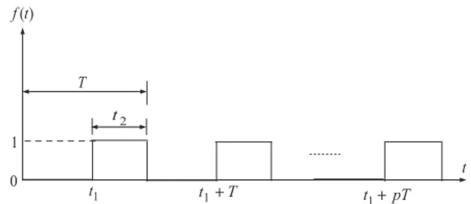
Figure 1 presents the PWM waveforms applied to power switches in conventional converters, in which [0, t1] and [ t1,T] are time intervals for Q2 and Q1 conduction. While the [0, t1] interval is DT, the [ t1,T] interval will be (1–D) T. f (t) is the PWM signal.
Figure 2 illustrates the conventional Z-source converter structure and equivalent circuits for switching period T. In the time interval in which Q1 is conducting, Q2 is the opened circuit and vice versa. This means that only one control circuit topology will be applied to power switches at the same time. In the first interval, while Q1 is closed, the input power supply and C2 will charge the inductors, and for the next interval, (1-D)T, inductors will play the role of sources and they will discharge. The inductor current and capacitor voltage reference directions are determined by considering the stable station relations.
1 t T 2 t T t1+ t1+pT ) (t f t 1 0
Figure 1. Pulse width modulation (PWM) applied to power switches. Per period (T), contains two (0,t1) and (t1,T) intervals.
(a) (b) (c)
Figure 2. (a) A quasi-Z-source converter structure; (b) when Q1 is conducting and (c) when Q2 is conducting.
According to these states, we can calculate the voltage gain of the structure [27] as in Eq. (1):
G = Vo Vin
= 1− 2D
1− D . (1)
The voltage value across C1 and also the ripple amplitude can be found as [27]: { VC1= 1−DD Vin= (1− M sin ωt)Vin ∆VC1=(1−D)TC sIL1 1 = − sin ωt+M(sin ωt)2T sIo (2−M sin ωt)C1 , (2)
and the following can be seen: IL1=−1−DD Io=−(sin ωt − M(sin ωt)2)Io, IL2=−IO, ∆IL1= ∆IL2= VinLT1sD = VinTs(1−M sin ωt) L1(2−M sin ωt) . (3)
In this condition, the output voltage value can be calculated as follows [1]:
ω = 2πf⇒ V o = V sin ωt. (4)
In Eq. (4), V, ω , and f are the inverter output voltage, angular velocity, and frequency, respectively. By considering duty cycle D, the output and input voltage relations are linear in all full bridge converters, so to get a sinusoidal output voltage, D must also be sinusoidal. However, the duty cycle is nonlinear in semi-Z-source
converters; consequently, it will be necessary to obtain an improved equation including the modulation index. According to Eq. (4), the modulation index can be defined as:
M = V
Vin
. (5)
Since the quasi-Z-source inverter’s voltage waveform is nonlinear, the reference wave can be rewritten as below:
D = 1− |M sin ωt|
2− |M sin ωt|, (6)
D′= 1
2− |M sin ωt|. (7)
D and D’ are the duty cycle values for switches Q1 and Q2, respectively. 1 0 -1 -2 -3 -4 -5 0.5 0.667 1 0 V o lt a ge G ai n Duty Cycle
Figure 3. Voltage gain curve of Z-source converter according to duty cycle [1].
Figure 3 illustrates the voltage gain curve for the quasi-semi-Z-source converter, which shows the duty cycle of Q1 [1]. Q1 and Q2 are working in such a way as to complement each other. With the operating of Q1 in the [0–0.66] interval, the converter can produce full bridge output voltage in [ +VIN, −VIN] limits. Output
voltage has positive values for (0 <D <0.5) and negative values for (0.5 <D<0.667). As can be seen for D = 0.5, the Z-source converter has no ability to produce the output voltage. Figure4presents the switches’ states by the proposed sinusoidal pulse width modulation (SPWM) method.
2.1. One-phase system
Although the gate signal for Q1 can be found by both of Eqs. (6) and (7), in this stage Eq. (7) is selected because of its simplicity. The modulation coefficient for the proposed SPWM can be changed within [0–1]. In the proposed control method, changing the ω t value, the sinusoidal voltage waveform will be obtained in the output. As explained before, duty cycle values will be limited to [0–0.66]. The Z-source converter can be extended to two phases, which will operate as a buck-boost converter. In this condition, duty cycle limits will change within [0–1] and voltage gain can increase double or triple times. Figures 5a–5d illustrate the proposed
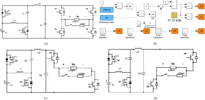
Figure 4. Generated SPWM for both power switches on quasi-Z-source side.
switching SPWM method for the one-phase Z-source converter structure and the states of the inverter side power switches for obtaining a sinusoidal voltage signal with 50 Hz frequency.
(a) (b)
(c) (d)
Figure 5. Combination of (a) quasi-Z-source converter and H bridge inverter and (b) proposed modified SPWM switching method typologies in one-phase system; (c) and (d) are the switching sequences for inverter switches.
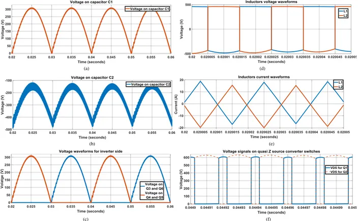
This figure presents the combination of the Z-source converter structure with the H bridge inverter. Simulation has been done in MATLAB/Simulink and the output voltage value has been adjusted to about 320 Vac root-mean-square (RMS) and 50 Hz. For the simulation, L1 and L2 values are selected as 130 mH and C1 = 1 µ F and C2 = 10 µ F. The reference voltage is compared with a carrier triangle wave with 25 kHz frequency. A voltage or current that is periodic but not purely sinusoidal will have higher frequency components in it, contributing to the harmonic distortion of the signal. By application of Fourier analysis in our study, we obtain about 1.51% THD for the one-phase system and a fixed value of load, since 2.23%–8.8% THD was reported in [2,15,24]. Figures5b and 5c illustrate the states of switches on the H bridge side and show that Q3 and Q4 are working in the same time interval while Q4 and Q5 will be active simultaneously in the next time interval to produce a sinusoidal voltage value for the load. Figure 6 shows the different voltages and current waveforms for quasi-Z-source and inverter components. Figures 6a and 6b show the voltage signals across C1
and C2, respectively. This figure illustrates that while a capacitor absorbs a positive voltage another one will absorb a negative value. Figure6c illustrates voltage waves of the inverter side power switches and can prove our claim of a pure sinusoidal voltage wave for the load. Figures 6d and 6e present the voltage and current waveforms for inductors and Figure6f shows the voltages stresses on quasi-Z-source power switches.
(a) (d)
(b) (e)
(c) (f)
Figure 6. Voltage waveform across (a) C1 and (b) C2 capacitors; (c) inverter side power switches; (d) L1 and L2
inductors; and current of (e) inductors and (f) voltage across the quasi-Z-source side power switches.
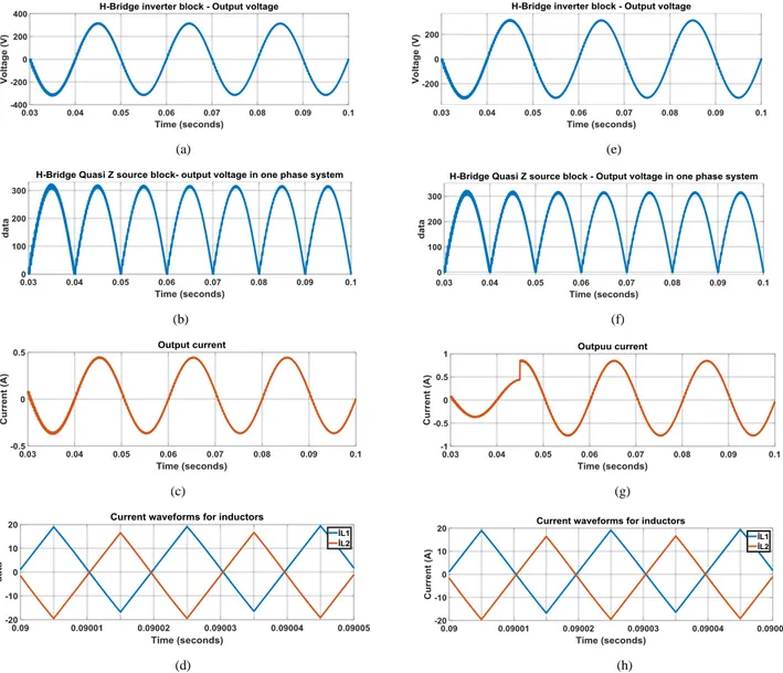
Figure7 comprehensively shows the main parameters of the converter for different types of loads in the one-phase system. At the first step a 0.5 kW resistive, QL = 100 VAR inductive, and QC = 50 VAR capacitive load is connected as the load to the inverter’s output. After 0.045 s the second load with the same value will connect to the output in parallel with the first load. This figure shows that the proposed switching method has a suitable performance and with the same voltage signal the current value will increase two times to supply both loads. Figure7a illustrates the output voltage of the proposed one-phase structure with a load that consists of a serial connection of 0.5 kW resistive, QL = 100 VAR inductive, and QC = 50 VAR capacitive components. Figure 7b presents the output voltage of the quasi-Z-source impedance converter that will be applied to the H bridge inverter as an input voltage signal. Figures 7c and 7d show the load and inductor current waves, respectively. The second column of Figure7illustrates the same values for the one-phase system by considering the second load. As can be seen from Figures 7e–7h, voltage signals are seen without a difference at a similar value and the current value has doubled in order to supply the total loads current.
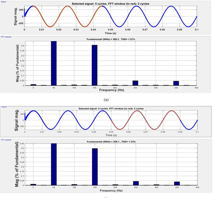
Figure8presents the THD analysis results for the one-phase system with the load value described above. Under the proposed modulation method, the output voltage has an acceptable THD value as shown in the figure with 1.51% THD for the first load (heavy load) and 1.33% for the next step (lighter load) and with the existence of both loads obtained.
(a) (e)
(b) (f)
(c) (g)
(d) (h)
Figure 7. One-phase system results: (a) output voltage waveform, (b) output voltage signal of quasi-Z-source converter, (c) output current waveform, and (d) inductor current signals considering the first load. (e) Output voltage waveform, (f) output voltage signal of quasi-Z-source converter, (g) output current waveform, and (h) inductor current signals when second load acts in parallel with the first load. Second load is applied at t = 0.045 s.
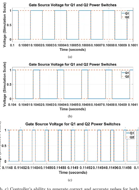
Figure9 illustrates the performance of the projected controller circuit; as can be seen, in different times of a switching period, the controller generates different pulses to switch on and off the power MOSFETs.
Figure 10shows a comparison between this approach and the proposed methods in [1], [20], and [26] for resistive loads. As can be seen, significantly better results are reported in the sinusoidal state. The method in [1] presents a controller that can trace the frequency deviations, but it seems that because of derivative operations it is slow. The method of [1] needs high DC voltages in the input block, and efficiency is higher for higher values of DC input voltages and lower for small DC voltages. The work in [26] presents an optimization of a buck-boost converter by applying a capacitor at the output of the converter and control of the switch is done by sampling the capacitor’s voltage, but in this study, by considering a fixed DC voltage at the input of the converter that can obtained by a boost converter, the switching method has been improved, and as the result,
(a)
(b)
Figure 8. Fourier analysis for one-phase approach at (a) 0.5 kW, QL =100 VAR, and QC = 50 VAR and (b) when the second load with the same value acts in parallel with the first load. Second load is applied at t = 0.045 s.
better THD values of output voltage and current signals for resistive and dynamic loads have been obtained. While the voltage waveform of capacitive loads can be the same as for the inductive loads, the current waveforms of capacitive loads completely depend on load conditions and values in any converter.
2.2. Two-phase system
In Eq. (8) and Eq. (9), V1 and V2 are the output voltage of the first and second blocks, respectively, and V12 is the output voltage. By considering the proposed two-phase Z-source topology and adjusting the modulation index per phase, by changing the input voltage VIN, output voltage magnitude will be fixed.
(a)
(b)
(c)
Figure 9. (a, b, c) Controller’s ability to generate correct and accurate pulses for both power switches.
(a) (b)
Figure 10. Comparison between proposed structure and methods presented in [1], [20], and [26] for quality tests for
the output voltage and current signals.
V1=|V sin(ωt)| , (8)
V12= Vac= V (|sin(ωt)| − |sin(ωt + 180)|) = 2V |sin(ωt)| . (10)
Figure 11. Extended two-phase structure with H-bridge inverter block for proposed method.
Figure 12. Combination of proposed controller, quasi-Z-source converter, and H-bridge inverter structures in two-phase mode.
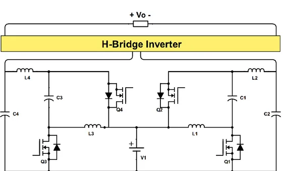
The next step of the simulation has been done for the two-phase topology with H bridge inverter. Figure11
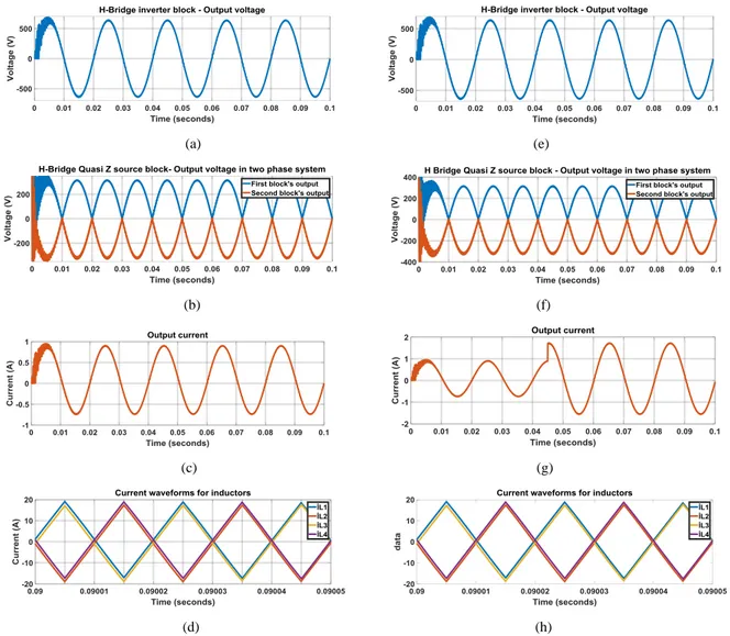
illustrates the connection between the extended two-phase system with the H bridge inverter block and output load. Figure 12shows the extended two-phase inverter structure with the controller diagrams. As can be seen, by considering the input voltage as 469 VDC, the output value will gain 625 Vac. Figures13a–13h illustrate the simulation results for the output voltage and current waveforms and output voltage and inductor currents of quasi-Z-source side waves of the extended two-phase topology for the first and second loads; as can be seen, when the second load is applied after 45 ms from the initial point, no considerable change appears in voltage waveforms but the load current signal will be about once greater. Also, for both quasi-Z-source blocks, generated voltage waveforms are shown, and it can be seen that the structure creates two symmetric and inverted waveforms at
the entrance of the H bridge inverter block. Figures13a and 13e illustrate the output voltage of the proposed two-phase structure with the same load used in the one-phase system, respectively. Figures13b and 13f show the output voltage of the dual quasi-Z-source impedance converter blocks that will be applied to the H bridge inverter as input voltage signal in the presence of the first and second loads, respectively. Figures 13c and 13g show the load current waves for these two different load values and it can be seen that the load current value has been doubled by the second load. Figures13d and 13h show the inductor current waveforms for both quasi-Z-source converter blocks.
(a) (e)
(b) (f)
(c) (g)
(d) (h)
Figure 13. Two phase system results: (a) output voltage waveform, (b) output voltage signals of quasi-Z-source converter blocks, (c) output current waveform, and (d) the inductor current signals for 0.5 kW, QL = 100 VAR, and QC = 50 VAR). (e) Output Voltage waveform, (f) output voltage signals of quasi-Z-source converter blocks, (g) output current waveform, and (h) inductor current signals when second load acts in parallel with the first load. Second load value is the same as the first load and is applied at t = 0.045 s.
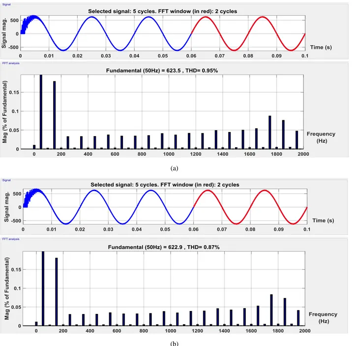
Figures 14a and 14b present the THD values for the output voltage in the two-phase system with the load values described above. For the first load 0.95% THD has been gained and for heavier loads and when the second load acts in parallel with the first load, the structure gives 0.87% THD.
(a)
(b)
Figure 14. Fourier analysis for two-phase approach at (a) 0.5 kW, QL = 100 VAR, and QC = 50 VAR and (b) when the second load with the same value acts in parallel with the first load. Second load is applied at t = 0.045 s.
3. Experimental results
To verify the theoretical and simulation results, a 120 W laboratory prototype has been implemented. Figure15
illustrates the proposed structure and controller circuit in the one-phase system. For this purpose, IXTQ460P2 power MOSFETs, two 130 µ H iron toroid core type inductors compatible with working to a maximum of 200 kHz, and two 1 µ F and 10 µ F capacitors respectively for C1 and C2 are applied. Converter components are selected to work at 120 W with about 660 V peak to peak AC output. The controller structure uses a
PIC12F629, 8 pin microcontroller, and TLP250 as the power MOSFET driver. As output load, two resistive loads with 1.8 K Ω and 600 Ω have been used for THD evaluation.
(a) (b) (c)
Figure 15. (a) Implemented prototype, (b) THD analysis for heavy loads, and (c) light loads in one-phase topology.
Two different loads have been selected to evaluate the performance of inverter ability to produce sinusoidal voltage and current waveforms. In the first stage, a 1.8 K Ω load has been selected in the structure’s output, and in the second state, a 600 Ω resistive load has been added in parallel with the first load. Figure 13illustrates the results. No change in voltage waveform is reported when the second load is placed in the circuit. Figure16a presents the current waveforms of the inductors. Around 250 mA of ripple has been reported for these currents. Figure16b illustrates the drain-source voltages across the quasi-Z-source power MOSFETs and Figure16c shows the voltage on the inverter side power switches. As can be seen, a waveform with 50 Hz frequency and 310 V peak value has been given across the power MOSFETs and it gives 620 Vac as output voltage across the load as illustrated in Figure 16d.
(a) (b) (c) (d)
Figure 16. (a) Inductor current waveforms, (b) drain-source stresses on power MOSFETs on quasi-Z-source side, (c) voltage signals of inverter side MOSFFETs, and (d) output voltage and current waveforms.
Figure17presents the efficiency diagram for the proposed switching method and the methods introduced in [1], [20], and [26]. Simulations have been done for all presented methods but only [1] has experimental results. 4. Conclusion
In this study, a modified SPWM technique is introduced for a Z-source-based inverter structure in order to get pure sinusoidal voltage and current waveforms for inductive and capacitive loads that can easily solve the nonlinear voltage gain problem with minimum THD. One of the most important advantages of the proposed method is applying the circuit with the optimal number of components for both inverter and controller struc-tures. Especially in RESs, this feature is critical since they produce low amounts of power. As previous studies
(a) (b) 80 85 90 91 81 86 88 90 82 85 89 90 81 86 88 91 50 W 80 W 100 W 120 W E ff ic ie n ce y
Output power value
[2] [15] [24] Proposed method 80 85 87 88 80 85 87 90 50 W 80 W 100 W 120 W E ff ic ie n cy
Output power value
[15] Proposed method
Figure 17. Efficiency comparison between proposed switching method and [1], [20], and [26] (a) according to (q)
simulation and (b) experimental results.
reported a THD rate of about 2.23% to 8.8%, 0.87% to 1.51% THD was obtained in this study for one- and two-phase topologies. One of the novel aspects of the proposed switching method is the absence of harmonic elimination circuits and strategies. In addition, unlike the traditional single-phase impedance source topologies, power switches of this structure are switched complementarily without applying any extra shoot-through state switching. As many of the new energy sources such as photovoltaic panels can produce limited values of input DC voltages and powers, high values of power losses can be reported because of the high amount of current in inductors. The proposed two-phase Z-source topology allows adjustment of the modulation index per phase by changing the input voltage VIN and has presented a switching method that fixes the output voltage at
about 310 Vac for dynamic loads by changing the load current according to load value at the expense of system complexity and cost. A group of simulations has been done in MATLAB/Simulink for both semi-Z-source and proposed switching structures. The 120 W implemented prototype’s test results confirm all the theoretical and simulation results. Where the output voltage and current waveforms present 50 Hz signals, optimized THD and a good level of quality for these waveforms have been gained.
Acknowledgment
Thanks to Assoc Prof Dr Mehmet Çelebi, who was my inspiration in this research. References
[1] Nourollah S, Pirayesh A, Fripp M. Multitier decentralized control scheme using energy storage unit and load management in inverter-based AC microgrids. Turk J Elec Eng & Comp Sci 2017; 25: 735-751.
[2] Shinde U, Kottagattu S, Kadwane S, Gawande S. Grid-connected quasi-z-source inverter with battery. Turk J Elec Eng & Comp Sci 2018; 26: 1847-1859.
[3] Villanueva E, Correa P, Rodriguez J, Pacas M. Control of a single-phase cascaded H-bridge multilevel inverter for grid-connected photovoltaic systems. IEEE T Ind Electron 2009; 56: 4399-4406.
[4] Kim JS, Kwon JM, Kwon BH. High-efficiency two-stage three-level grid-connected photovoltaic inverter. IEEE T Ind Electron 2018; 65: 2368-2377.
[5] Panda AK, Suresh Y. Performance of cascaded multilevel inverter by employing single and three-phase transformers. IET Power Electron 2012; 5: 1694-1705.
[6] Li RTH, Chung SH. Digital boundary controller for single-phase grid-connected CSI. In: IEEE 2008 Power Elec-tronics Specialists Conference; 15–19 June 2008; Rhodes, Greece. New York, NY, USA: IEEE. pp. 4562-4568.
[7] Ansari SA, Skandari A, Milimonfared J, Moghani JS. A new control method for an interleaved fly-back inverter to achieve high efficiency and low output current THD. In: IEEE 2018 Annual Power Electronics, Drives Systems and Technologies Conference; 14–15 February 2018; Tehran, Iran. New York, NY, USA: IEEE. pp. 89-94.
[8] Kim M, Han BL, Son S, Kim S, Kim JS, Kim JS, Pohang HK. Iterative learning controller for fly-back inverter. In: IEEE 2018 Applied Power Electronics Conference and Exposition; 4–8 March 2018; San Antonio, TX, USA. New York, NY, USA: IEEE. p. 2973.
[9] Han B, Ledwich G, Karaday G. Study on resonant fly-back converter for DC distribution system. IEEE T Power Deliver 1999; 3: 1069-1074.
[10] Lydia J, Wimalraj SLS, Aishwariya A. Implementation of photovoltaic inverter for high power agricultural appli-cations using interleaved fly-back topology. In: IEEE 2016 Technological Innovations in ICT for Agriculture and Rural Development; 15–16 July 2016; Chennai, India. New York, NY, USA: IEEE. pp. 51-57.
[11] Chen Y, Xu D, Xi J, Hu G, Du C, Li Y, Chen M. A ZVS grid-connected full-bridge inverter with a novel ZVS SPWM scheme. IEEE T Power Electron 2016; 31: 3626-3638.
[12] Asl ES, Babaei E, Sabahi M, Nozadian MHB, Cecati C. New half-bridge and full-bridge topologies for a switched-boost inverter with continuous input current. IEEE T Ind Electron 2018; 65: 3188-3197.
[13] Yamaguchi D, Fujita H. A new PV converter for a high-leg delta transformer using cooperative control of boost converters and inverters. IEEE T Power Electron 2018; 33: 9542-9550.
[14] Dahidah MSA, Agelidis VG. Single-carrier sinusoidal PWM-equivalent selective harmonic elimination for a five-level voltage source converter. J Electr Power Syst Res 2008; 78: 1826-1836.
[15] Sun RH, Sun YH, Ik HJ. Carrier-based signal injection method for harmonic suppression in PWM inverter using single DC-link current sensor. In: IEEE 2006 IECON 32nd Annual Conference; 6–10 November; Paris, France. New York, NY, USA: IEEE. pp. 2700–2705.
[16] Schmidt H, Siedle C, Kettere J. DC/AC converter to convert direct electric voltage into alternating voltage or into alternating current. US Patent US7 046 534 B2, 2006.
[17] Xiao H, Xie S, Chen Y, Huang R. An optimized transformerless photovoltaic grid-connected inverter. IEEE T Ind Electron 2011; 58: 1887-1895.
[18] Siwakoti YP, Blaabjerg F. Common-ground-type transformerless inverters for single-phase solar photovoltaic sys-tems. IEEE T Ind Electron 2018; 65: 2100-2111.
[19] Filizadeh S, Gole AM. Harmonic performance analysis of an OPWM-controlled STATCOM in network applications. IEEE T Power Deliver 2005; 20: 1001–1008.
[20] Qin L, Hu M, Lu DDC, Feng Z, Wang Y, Kan J. Buck–boost dual-leg-integrated step-up inverter with low THD and single variable control for single-phase high-frequency AC microgrids. IEEE T Power Electron 2018; 33: 6278–6291. [21] Amamra SA, Meghriche K, Cherifi A, Francois B. Multilevel inverter topology for renewable energy grid integration.
IEEE T Ind Electron 2017; 64: 8855–8866.
[22] Khamooshi R, Namadmalan A. Converter utilisation ratio assessment for total harmonic distortion optimisation in cascaded H-bridge multi-level inverters. IET Power Electron 2016; 9: 2103–2110.
[23] Zheng L, Jiang F, Song J, Gao Y, Tian M. A discrete-time repetitive sliding mode control for voltage source inverters. IEEE J Em Sel Top P 2018; 6: 1553–1566.
[24] Liu T, Wang D. Parallel structure fractional repetitive control for PWM inverters. IEEE T Ind Electron 2015; 62: 5045–5054.
[25] Zhao Q, Ye Y. A PIMR-type repetitive control for a grid-tied inverter: structure, analysis, and design. IEEE T Power Electron 2018; 33: 2730–2739.
[26] Celebi M, Alan I. A novel approach for a sinusoidal output inverter. Electr Eng 2010; 92: 239–244.
[27] Ahmed T, Mekhlef S. Semi-Z-source inverter topology for grid-connected photovoltaic system. IET Power Electron 2015; 8: 63-75.
![Figure 3. Voltage gain curve of Z-source converter according to duty cycle [ 1 ].](https://thumb-eu.123doks.com/thumbv2/9libnet/4016528.55386/5.918.287.628.436.701/figure-voltage-gain-curve-source-converter-according-cycle.webp)
