Intimate Monolithic Integration of Chip-Scale
Photonic Circuits
Vijit A. Sabnis, Member, IEEE, Hilmi Volkan Demir, Member, IEEE, Onur Fidaner, Student Member, IEEE,
Jun-Fei Zheng, James S. Harris, Jr., Fellow, IEEE, David A. B. Miller, Fellow, IEEE, Nelson Li, Ta-Chung Wu,
H.-T. Chen, and Yu-Min Houng
Abstract—In this paper, we introduce a robust monolithic in-tegration technique for fabricating photonic integrated circuits comprising optoelectronic devices (e.g., surface-illuminated pho-todetectors, waveguide quantum-well modulators, etc.) that are made of completely separate epitaxial structures and possibly reside at different locations across the wafer as necessary. Our technique is based on the combination of multiple crystal growth steps, judicious placement of epitaxial etch-stop layers, a care-fully designed etch sequence, and self-planarization and passi-vation steps to compactly integrate optoelectronic devices. This multigrowth integration technique is broadly applicable to most III–V materials and can be exploited to fabricate sophisticated, highly integrated, multifunctional photonic integrated circuits on a single substrate. As a successful demonstration of this technique, we describe integrated photonic switches that consume only a 300 × 300 µm footprint and incorporate InGaAs photodetector mesas and InGaAsP/InP quantum-well modulator waveguides sep-arated by 50 µm on an InP substrate. These switches perform electrically-reconfigurable optically-controlled wavelength conver-sion at multi-Gb/s data rates over the entire center telecommuni-cation wavelength band.
Index Terms—Integrated optoelectronic devices, monolithic in-tegration, photonic switches, selective area growth (SAG).
I. INTRODUCTION
C
URRENT optical networks require the use of discrete optical and electronic components for performing optical–electronic–optical (OEO) conversion functions such as sending, receiving, regenerating, processing, and routing data. Chip-level integration of electronic and photonic devices on a single substrate increases the reliability, enhances the chip yield, simplifies the design, and reduces the size, power consumption, and cost of OEO conversion. In general, chip-level integrationManuscript received March 15, 2005; revised October 18, 2005. This work was supported by Intel Corporation.
V. A. Sabnis was with the Department of Electrical Engineering, Stanford University, Stanford, CA 94305 USA. His is now with Translucent, Inc., Palo Alto, CA 94303 USA (e-mail: [email protected]).
H. V. Demir was with the Department of Electrical Engineering, Stanford University, Stanford, CA 94305 USA. He is now with the Department of Physics and the Nanotechnology Research Center, Bilkent University, Ankara 06800, Turkey (e-mail: [email protected]).
O. Fidaner, J. S. Harris, Jr., and D. A. B. Miller are with the Department of Electrical Engineering, Stanford University, Stanford, CA 94305 USA (e-mail: ofi[email protected]; [email protected]; [email protected]).
J.-F. Zheng is with Intel Corporation, Santa Clara, CA 95052 USA (e-mail: [email protected]).
N. Li, T.-C. Wu, H.-T. Chen, and Y.-M. Houng are with OEPIC Corpora-tion, Sunnyvale, CA 94089 USA (e-mail: [email protected]; [email protected]; [email protected]; [email protected]).
Digital Object Identifier 10.1109/JSTQE.2005.860995
can be accomplished through either hybrid or monolithic techniques. Hybrid techniques, such as flip-chip bonding, combine multiple devices fabricated on different substrates into a single package. On the other hand, monolithic integration fabricates all devices simultaneously on a single substrate, akin to the manufacturing of silicon integrated circuits. In this case, external interconnection of individual devices is eliminated, and design and testing are performed for the overall integrated system. Furthermore, for high-speed applications, in contrast to hybrid integration, monolithic integration can offer substantial performance advantages by avoiding the use of solder bumps and long metal posts. Since interdevice distances can be minimized and external wire bonding is not required, parasitic resistance, capacitance, and inductance are minimized, pro-viding significant simplifications and improvements in design flexibility and ultimate circuit performance.
Currently, only group III–V material systems, such as GaAs and InP, along with their compatible ternary or quaternary alloys, can be used to fabricate high-speed, high-performance electronic and photonic devices suitable for data processing. Complex monolithic integration of different group III–V devices on a single substrate, however, is a relatively immature technol-ogy. Most researchers have focused on monolithic integration techniques that allow fabricating multiple optical devices along a single or set of optical waveguide(s) [1]–[3], for example, diode lasers integrated with electroabsorption modulators and semiconductor optical amplifiers. In these demonstrations, the integrated devices have similar device and epitaxial structures with the exception of the inclusion or exclusion of athin active layer located in the core of the shared waveguide. Other researchers have investigated integrating p-i-n photodiodes with electronic amplification and signal processing circuitry in which a single set of epitaxial layers is grown and then processed [4]. In this work, we developed and demonstrated a monolithic process for on-chip intimate integration of a waveguide electroabsorption modulator (EAM) and a surface-illuminated
p-i-n diode mesaphotodetector (PD), both of which consist
of completely different epitaxial layers except for the starting layers, along with other components to make a high-speed optically-controlled optical switch [5], [6]. We report a multi-growth monolithic integration technique [7] that incorporates a special etch sequence and self-planarization and passivation [8], [9] steps to enable chip-scale photonic circuit integration. To the best of our knowledge, few other groups have recently attempted to integrate surface-illuminated and waveguide-coupled opto-electronic devices monolithically on a single chip [10]–[13].
Fig. 1. Circuit diagram and principle of operation of PD-EAM photonic inte-grated circuit [6].
This integration technique forms the basis for application to other complex multifunctional photonic integrated circuits.
In Section II, we outline the device concept briefly and the integration requirements in detail. (More information on the device operation and testing can be found in [5], [6], [14]). In Section III, we describe and illustrate our monolithic integration process, comprising a two-step epitaxial growth sequence, the etch techniques used to define the PD mesas and EAM waveguides, device planarization and passivation, thin film resistor deposition, and metal interconnection. For validation of this integration technique, in Section IV we present proof-of-concept experimental results of high-speed optical switching and wavelength conversion from our devices before concluding in Section V.
II. PHOTODIODE-MODULATORPHOTONIC
INTEGRATEDCIRCUITS
A. Integrated PD-EAM Switch Concept
Fig. 1 shows the circuit diagram of a PD-EAM photonic inte-grated circuit [6]. This circuit, in effect, performs ultra-compact OEO conversion without the use of traditional receiver and trans-mitter electronic circuitry. The surface-normal input control data stream operating at a wavelengthλ1is incident on the
photode-tector. In the presence of the control data stream (i.e., an optical 1 bit), the PD generates a photocurrentIPDthat reduces the net
reverse bias across the EAM. Consequently, the optical trans-mission of a continuous-wave signal beam at a wavelengthλ2
that is edge-coupled into the waveguide EAM increases and the corresponding optical 1 bit is observed at the output. In the ab-sence of the control data stream on the PD (i.e., an optical 0 bit), the optical transmission ofλ2through the EAM remains low, resulting in a corresponding optical 0 bit at the output. The modulation in the EAM is achieved through the quantum confined Stark effect [15].
For switch operation, the PD is reverse-biased to ensure high-speed photocurrent extraction, while the EAM is reverse-biased such that quantum wells located in the core of the waveguide strongly absorb atλ2. The switching bandwidth, neglecting
par-asitics, is controlled by the RC time constant of the internal circuit and is given by (1) [6]:
f3 dBe=
√
3
2πRTF(CPD+ CEAM).
(1)
Both the PD and the EAM are fabricated from p-i-n diode structures and are independently reverse-biased through a pair of voltage supplies,VS-PD andVS-EAM, respectively. Biasing for both devices is provided across two large bypass capaci-tors(CBP), ∼ 500 pF, to ensure that the high-speed electronic
switching is localized to the integrated circuitry between both capacitors. The PD and EAM circuits are coupled through a thin-film resistor(RTF), which is connected between the shared
p-contact of the PD-EAM and ground (GND).
The PD-EAM photonic integrated circuit provides optical switching, wavelength conversion, multi-wavelength broadcast-ing, partial optical regeneration, space switchbroadcast-ing, and packet switching, all possibly provided at the same time for multiple channels on a single integrated chip [5], [6], [14], [16], [17]. It features multi-gigabit per second switching operation over the entire center telecommunication wavelength band (C-band) while requiring only milliwatt-level optical/electrical switching powers. Furthermore, our integration technique enables com-pact circuit integration into an area of only 300× 300 µm. A single packaged chip of the PD-EAM photonic integrated cir-cuit could displace, in certain optical networking applications, multiple discretely-packaged and interconnected electronic and optical components found in traditional OEO conversion modules.
B. PD-EAM Switch Circuit-Integration Requirements
The integration requirements of our PD-EAM photonic grated circuit are typical in that the implementation of any inte-grated, high-speed photonic circuit requires compact integration and low parasitics. For the PD-EAM switch, a monolithic pro-cess must intimately fabricate the entire circuit in a size scale much smaller than the wavelength of any of the electrical fre-quencies involved, enabling the switch to operate as a lumped circuit and precluding the need for incorporating transmission lines or other microwave circuitry inside the device. Electrical parasitics that unnecessarily degrade the device switching band-width and increase the required optical switching power are also minimized by such an intimate integration process. More-over, the integration technique must incorporate PD and EAM structures comprising separately optimizable epitaxial layers for better performance, including bi-directional wavelength con-version. This also eliminates other problems associated with a single diode implementation of such a switch [18]. Finally, the integration technique must also conveniently enable fabricating two-dimensional arrays of devices and possess scalability for high-speed switching operation.
Hybrid integration techniques can be used to construct the PD-EAM photonic integrated circuit and are attractive because they allow each circuit component to be individually designed and processed prior to integration, reducing the overall fab-rication tolerances and risks. The simplest hybrid integration approaches are to wire bond or flip chip bond a separately fab-ricated PD chip, EAM chip, and resistor chip together into the circuit shown in Fig. 1. Such techniques are relatively easy to implement, though they should be considered only as prelimi-nary solutions due to the problems associated with them. Wire
bonding increases the overall circuit size and both techniques introduce unwanted capacitance and inductance, thereby in-creasing the required optical switching power and potentially introducing design complexity through the introduction of un-necessary electrical impedance in the circuit. Indeed, unless the wire bond is very short, such awire bonded switch will not work due to the added capacitance of the wire. Although these concerns may not be problematic for switch operation up to a few Gb/s, they will substantially deteriorate the switching per-formance at speeds of 10 Gb/s and beyond. Furthermore, wire bonding is not practically feasible for constructing large two-dimensional (2-D) matrices of PD-EAM photonic integrated circuits.
Monolithic integration techniques can also be used to fabri-cate the PD-EAM photonic integrated circuit without compro-mising scalability for high-speed and 2-D array operation. The most straightforward monolithic integration technique requires growing the EAM and PD epitaxy on top of each other in a sin-gle growth step, creating, for example, a p-i-n-p-i-n or n-i-p-i-n diode stack. This method introduces amultilevel mesastructure and creates several challenges for lithography, where depth-of-focus limitations may create difficulties in patterning the various circuit components, and electrical interconnection, where multi-level routing of electrical interconnect metal would be required. Furthermore, such an approach introduces parasitics, again de-grading the speed performance of the integrated device, through the introduction of capacitance from unused diode epitaxy that is unnecessarily incorporated into the circuit. To avoid these problems, we developed a monolithic integration technique that we discuss in the next section. The technique employs selective area growth (SAG) [19]–[22] based on metal-organic chemical-vapor deposition (MOCVD) [23]. This approach enables ap-proximately planar, side-by-side integration of separate PD and EAM structures, without compromising individual component design.
III. MONOLITHICINTEGRATIONPROCESS
A. PD-EAM Integration Overview
There are five main features of our integration process: a) the incorporation of buried epitaxial etch stops for proper SAG sur-face preparation and device isolation; b) a selective area growth process that enables compact integration of different epitaxial structures; c) an SAG epitaxy etch technique employing selec-tive wet etches and shallow dry etches for creating device mesas in the SAG area; d) a polymer planarization and passivation pro-cess that ensures device reliability and enables electrical inter-connection of different devices; and e) a planarization-polymer etch process that allows multilevel metal routing as required by the circuit architecture. As an example of these integration techniques, in the following sections, we discuss how the above techniques are used to enable robust monolithic integration of PD-EAM photonic integrated circuits.
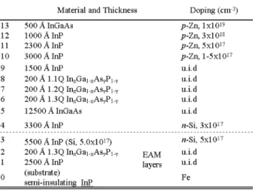
Tables I and II show the EAM and PD epitaxial layer struc-tures, respectively. A detailed discussion of the epitaxial layer design can be found in [6]. The EAM is a p-i-n-diode waveg-uide structure containing ten strained-InGaAsP quantum wells
TABLE I
EAM EPITAXIALLAYERSTRUCTURE
TABLE II
PD EPITAXIALLAYERSTRUCTURE
designed to provide efficient electroabsorption over the C-band. The PD epitaxy starts on top of layer 3 of the EAM epitaxy and comprises a p-i-n-diode surface-illuminated photodetector structure with an InGaAs intrinsic layer that provides broadband photoabsorption for wavelengths smaller than 1650 nm.
Fig. 2 shows a summary of the first several steps of the PD-EAM photonic integrated circuit process. Instead of consecu-tively growing the EAM and PD epitaxial layers in a single step, an epitaxial regrowth step is used to incorporate the PD layers after growth and modest processing of the EAM layers. Af-ter growing the EAM epitaxial layers on a semi-insulating InP wafer [see Fig. 2(a)], the wafer is dry-etched to create a periodic array of EAM ridge waveguides [see Fig. 2(b)] and encapsulated in a dielectric material [see Fig. 2(c)]. The PD epitaxy layers
Fig. 2. Selective area growth process for integrating PD and EAM: (a) EAM epitaxial growth, (b) EAM ridge etch, (c) SAG SiN nitride mask definition, (d) PD SAG, and (e) PD mesa etch. Not drawn to scale.
are then deposited using an SAG process employing MOCVD [see Fig. 2(d)]. The PD mesas are subsequently etched in the area adjacent to the EAM [see Fig. 2(e)], resulting in intimate integration of both components. The advantage of this imple-mentation is that the overall final structure can be designed to be approximately planar and, hence, it is significantly more straightforward to process than a single-step epitaxially grown structure. Subsequent steps complete the device integration by providing dielectric (e.g., polymer) planarization-passivation of the devices, thin film resistor deposition, and appropriate metal interconnection and routing.
B. Buried Etch-Stop Layers for SAG Surface Preparation
A key feature of the PD and EAM structures is the use of buried etch stop layers. These etch stop layers enable robust integration of different epitaxial layers by providing the ability to achieve clean, planar surfaces prior to epitaxial regrowths or after mesa/ridge etching. For the PD-EAM photonic integrated circuit a200- ˚A-thick 1.3Q etch-stop layer (Table I layer #4) is located part way into the bottomn-doped EAM cladding and a second etch-stop layer (Table I layer #2), shared with the PD, is located underneath the bottom waveguide cladding. Fig. 3 shows astain-etched cross section of the EAM ridge waveguide area, clearly showing the buried etch-stop layers.
After the growth of the EAM epitaxial layers, the wafers are masked with SiN and patterned into stripes. The EAM ridge waveguides are then created using an inductively-coupled reactive-ion etch using Cl2 and HBr gases. The etch depth is
chosen so that the ridge height falls into the upper part of the
n-doped InP cladding layer (Table I layer #5), but above the
Fig. 3. Scanning electron microscope (SEM) picture of stain-etched EAM waveguide area. The two dark lines running horizontally within the lower waveg-uide cladding are each 200- ˚A-thick 1.3Q etch-stop layers.
1.3Q etch-stop layer (Table I layer #4). The ridge waveguides and 5–10µm of surrounding area are subsequently masked off with another SiN layer to prepare for SAG. A selective InP wet etch (1 HCl: 3 H3PO4) is used to remove the remaining InP
in layer #5, stopping on the 1.3Q stop layer. The etch-stop layer ensures a clean surface with approximately perfect uniformity over the entire wafer surface, which is critical for achieving reproducible SAG results. Finally, a selective 1.3Q etch (1 H2SO4:8 H2O2:40 H2O) is used to remove the etch-stop layer, exposing a clean InP layer over the entire wafer and allowing the wafer to be regrown on using SAG.
This technique can be generalized for devices requiring mul-tiple SAG steps. For devices sharing a common bottom-doped epitaxial layer, multiple etch-stop layers—one for each SAG step—can be buried within the common doped layer to enable sequential surface preparation for SAG. For devices requiring different doping types or levels for their bottom layers, these different doped layers need to be grown sequentially in the first epitaxial growth step with a buried etch-stop layer located in each appropriate layer. Furthermore, this technique should also be applicable to the GaAs–AlGaAs-based material system. In this case, InGaP lattice matched to GaAs can serve as a selec-tive etch-stop layer since it is not attacked by most wet etch chemistries used to remove GaAs–AlGaAs materials.
C. Selective Area Growth Integration
We performed a series of studies to understand the charac-teristics and capabilities of SAG and to achieve a robust and reproducible SAG process. The MOCVD growths were per-formed using a Thomas Swan close-coupled showerhead reac-tor employing trimethylindium (TMIn) gas as the In source, trimethylgallium (TMGa) as the Ga source, 100 ppm Si2H6/H2 as the Si source, diethylzinc (DZ) as the Zn source, AsH3as the
As source, PH3as the P source, and H2as the carrier gas. The
epitaxy was grown at 650◦ C at a growth pressure of 100 torr. The carrier gas flow was∼20 lpm, the V–III flow rate ratio was
∼100, and the substrate rotation during growth was 100 rpm.
Fig. 4 shows aSEM picture of aportion of aregrown wafer. The thin stripe crossing through the center of the picture is the
Fig. 4. SEM picture showing PD SAG epitaxy adjacent to SiN-masked EAM ridge waveguide area.
EAM ridge waveguide, which runs continuously from one end of atwo inch wafer to the other end. Aw = 15 µm wide SiN mask encapsulates the waveguide, and this masked area repeats laterally every 500µm across the entire width of the wafer. The areas outside the SiN masked area contain selectively grown PD epitaxy.
By examining such wafers, we find that there are three main characteristics of SAG that are necessary to consider for com-pactly integrating the PD and EAM. The composition of the ma-terial grown near the SAG mask edge is different than it is at loca-tions far from the mask edge. For InGaAs and InGaAsP growths, epitaxy near the mask edge incorporates a larger In mole frac-tion, resulting in compressive strain and large shifts in bandgap energy. This compositional variation gradually tapers off with increasing distance from the mask edge. This characteristic can be advantageous for integrating active and passive waveguide devices on chip, but in our case we need to avoid this region to en-sure reliable and high-performance PD operation. The enhanced In incorporation can be explained by the lower decomposition temperature of TMIn gas compared with TMGa gas, resulting in a higher concentration and effective diffusion coefficient of In species. Since deposition does not occur on the SAG mask, there is a larger proportion of In species near the mask edge than further away. An alternative explanation [19] suggests that it is easier to break a methyl–indium bond compared to a methyl– gallium bond at the substrate surface, allowing for the increased incorporation of In compared to Ga near the mask edge.
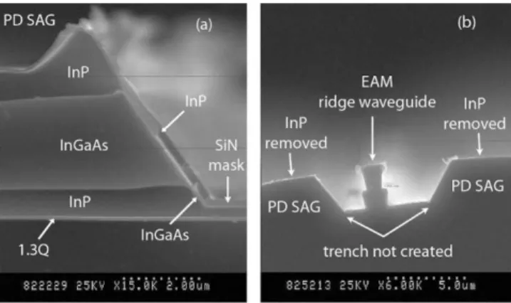
The second major characteristic of SAG is that each epitaxial layer completely encapsulates all underlying SAG layers. This is particularly important at the interface between the SAG area and the masked area; the encapsulation can be seen very clearly in Fig. 5(a), which shows a SEM cross-sectional picture of stain-etched PD SAG epitaxy adjacent to the SiN-masked EAM waveguide area. In this figure the upper InP layer seals the InGaAs absorber layer at locations far from the mask edge where the SAG epitaxy shape is stable and continues to do so all the way to the interface with the SiN mask where the SAG epitaxy exhibits a sloped shape. Similarly, the InGaAs absorber seals the
Fig. 5. (a) SEM picture of stain-etched PD SAG epitaxy where each epitaxial layer encapsulates lower layers and (b) PD SAG epitaxy after removal of upper InP layer using a selective wet etch. The etch does not create a trench at the interface between the SAG and masked-EAM areas, confirming encapsulation of SAG layers.
lower InPn-doped layer. Fig. 5(b) confirms the epitaxial-layer encapsulation by showing the PD SAG area after the sample has been dipped in a selective InP etch. The upper InP layer of the PD epitaxy has been removed without damage to the underlying layers. In particular, a trench has not been created at the SiN mask edge, which would preclude convenient routing and interconnection of the EAMn-metallization. In this case, the trench can not be created since the InGaAs layer grown prior to the upper InP layer is present at the interface with the SiN mask.
As can be seen in Figs. 4 and 5, the third major characteristic of SAG is an increased growth rate near the SAG mask edge. This enhancement is caused by lateral vapor phase diffusion above the SAG mask that supplies additional reactants to the unmasked area. The SAG growth rate is a strong function of the width of the SAG mask and the width of the unmasked area. As the SAG mask width increases, the growth rate near the mask edge increases due to the increase in lateral supply of reactants coming from the masked area. Similarly, as the width of the unmasked region decreases, the SAG growth rate near the mask edge also increases since the lateral supply of reactants from the masked area is consumed over the smaller unmasked area. There is a strong crystallographic dependence on the shape of the regrown epitaxy. In Fig. 4, the EAM waveguides are oriented in the (011) direction. The sloped area near the SAG mask edge corresponds to the (111)B crystal plane. Epitaxy grows slower on this plane than on the (001) plane because the dangling bond density of the (111)B plane is approximately 42% lower than on the (001) plane [19]. During growth, Group III reactants migrate from the lower bonding density (111)B plane to the higher bonding density (001) plane, creating the spiked-shape feature near the mask edge.
We designed our integration process to incorporate the PD epitaxy after the growth of the EAM epitaxy, rather than the opposite order, to avoid complications arising from the thick-ness and composition characteristics of SAG. The EAM epitaxy contains strained-InGaAsP quantum wells with an absorption band edge located approximately at 1480–1490 nm. Integrating
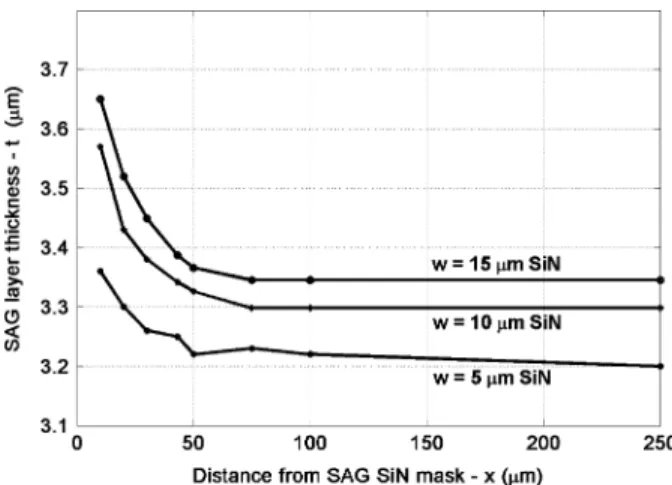
Fig. 6. Thickness of SAG epitaxy(t) versus distance from SiN SAG mask (x) for three SAG masks widths (w).
the EAM using SAG may produce thicker quantum wells with a larger In content, resulting in a displaced absorption band edge and reduced electroabsorption performance. Although these ef-fects could be eliminated or compensated through an extensive set of SAG studies, it is easier and less risky to perform SAG of the PD epitaxy. Furthermore, the PD photodetection charac-teristics are not extremely sensitive to the exact thickness of the absorbing intrinsic region, which is made up of InGaAs lattice-matched to InP. The main requirement is that the PD needs to be fabricated far enough away from the mask edge to ensure that the InGaAs is not highly strained, ensuring reliable PD operation with strong absorption over the C-band.
In order to determine the minimum distance that the PD and EAM can be fabricated from each other, we measured the thick-ness,t, of the SAG epitaxy as a function of distance from the mask edge, x, for 5, 10, and 15 µm SiN SAG mask widths,
w, using scanning electron microscopy (see Fig. 4). Although
this measurement does not provide information about the strain present in the SAG epitaxy, for this particular geometry, it is a reasonable assumption that the epitaxial compositional variation approximately follows the SAG thickness variation. Fig. 6 shows a plot of the SAG epitaxial thicknesst versus x for 5-, 10-, and 15-µm SAG mask widths. As expected, as the mask width in-creases, the SAG thickness enhancement increases. For all three mask widths, the SAG thickness stabilizes after approximately 50µm, although the stabilized thickness is different for each mask width, indicating an overall thickness enhancement com-pared to growth on an unmasked substrate. From these results, we can conservatively estimate a minimum required separation of 50µm between the PD and EAM. This is a relatively small spacing, and the necessary 50-µm-long electrical interconnect between the PD and EAM will not introduce any significant electrical parasitics. If we consider 50µm to be the minimum size-scale limit for integration of the various circuit components, lumped-circuit operation of such integrated optoelectronic cir-cuits up to 40 Gb/s should be achievable since the electrical wavelength at these speeds is approximately 2 mm, which is more than 10 times larger than the minimum device separation. Hence, this selective area growth technique provides for
com-pact integration of the optoelectronic components that should easily accommodate high-speed operation.
For the PD-EAM switch integration we designed the thickness of the PD epitaxy to be approximately 2500 ˚A thinner than the EAM epitaxy to compensate for the thickness enhancement provided by SAG. This allows the uppermost surfaces of the PD and EAM to be approximately planar after SAG, making subsequent polymer planarization and electrical interconnection convenient. Note that in general, epitaxial structures from different growth steps can be de-signed so that they are approximately planar with each other through the incorporation of dummy or sacrificial layers (i.e., doped or undoped InP–GaAs, depending on the material system used).
D. SAG Epitaxy Patterning
In many cases, SAG will result in modified growth features near the SAG mask edge, as shown in Figs. 4 and 5, which can be problematic for device integration. Although fabricating mesa structures in the SAG area does not present any unique challenges by itself, it is often times desirable or necessary to create these mesas while simultaneously creating a planar in-terface between the SAG area and the masked area to allow for convenient interconnection of devices residing in these different growth areas. The modified growth features near the mask edge often complicate this requirement since a simple nonselective mesaetch in the SAG areawill not produce the desired inter-face; for example in the case of Fig. 5(b) a trench would be created at the interface. The encapsulation of the SAG epitaxy, as discussed in the previous section, is critical because it enables one to use a series of selective wet etches [24] and shallow dry etches to fabricate mesas in the SAG area, while creating an approximately smooth, planar surface at the SAG interface. The selective wet etches allow the SAG epitaxial layers to be re-moved sequentially, while the shallow dry etches are used only to remove layers that are difficult to wet etch selectively.
For the PD-EAM switch, once the PD SAG is completed, SiO2 is deposited and patterned as a mask for the PD mesas.
We etch the PD mesas [see Fig. 2(d)] using a five-step sequence of dry and wet etches. A selective InGaAs etch (1 H2SO4:8
H2O2:40 H2O) removes the top InGaAs p-contact layer (Table II
layer #12), followed by a selective InP etch (1 HCl: 3 H3PO4)
that etches down to the graded quaternary layers (Table II layer #8). Next, a short reactive ion etch using a methane-hydrogen-argon gas chemistry [25] removes the graded quaternary layers (Table II layers #6–8), stopping a few hundred angstroms in-side the InGaAs absorber region. A long selective InGaAs(P) etch (1 H2SO4:8 H2O2:40 H2O) removes the InGaAs absorber region (Table II layer #5). During SAG, the interface between the bottomn-doped InP layer and the InGaAs absorber is not abrupt, resulting in a parasitic InGaAsP interfacial layer. The degree of phosphorous incorporation is more severe near the SAG mask edge than further away, resulting in an InGaAsP layer whose thickness tapers off with increasing distance from the mask edge. In order to remove this layer, we significantly overetch on this step, creating a lateral undercut of the InGaAs
Fig. 7. SEM picture of PD mesa after mesa etching, planarization, and p-metal deposition.
absorber region within the PD mesa. This undercut, however, is advantageous because it ensures complete encapsulation of the intrinsic region by the planarization/passivation material (bisbenzocyclobutene—BCB) that is applied and etched back in a later processing step. The undercut additionally reduces the PD capacitance, improving switching performance [8]. Finally, a second shallow reactive ion etch removes any remaining par-asitic InGaAsP and continues approximately 1000 ˚A within the underlyingn-doped InP layer (Table II layer #4). Fig. 7 shows across-sectional SEM picture of afinished PD structure. Most importantly, this process creates a smooth interface between the PD SAG area and the EAM area since primarily selective wet etches are used to create the PD mesas. This technique can be generally applied to devices where the mesa sidewall profile created by selective wet etches is not deleterious. If perfectly straight sidewalls are required, then it is likely that an alternate etching technique must be used.
E. Buried Etch-Stop Layers for Device Isolation
A second use for the buried etch-stop layers is to assist in pro-viding device isolation. Once the various mesas in the different regions of the wafers have been created, it is typically necessary to electrically isolate the individual devices. By burying an etch-stop layer below all the doped device layers, one can easily use selective wet etching to create electrical-isolation mesas around the individual devices which extend into a nominally undoped layer or semi-insulating substrate.
For the PD-EAM switch integration, after the PD mesa def-inition, the surrounding areas of the PD and EAM are masked off with photoresist to define the n-regions of both devices. We employ athree-step wet etch sequence to isolate the PD and EAM devices from each other. First, a selective InP etch (1 HCl: 3 H3PO4) removes the exposedn-doped InP material (Table II layer #4-#3), stopping on the bottom etch-stop layer (Table II layer #2). The presence of the bottom etch-stop layer ensures that a planar, uniform etch depth is achieved over the entire sample area, despite the different starting thicknesses of the n- doped InP in the PD and EAM areas. Second, a selec-tive InGaAsP etch (1 H2SO4:8 H2O2:40 H2O) removes the
bottom etch-stop layer, and finally a subsequent selective InP etch (1 HCl: 1 H2O) removes the unintentionally doped InP
buffer layer (Table II layer #1) and continues a few thousand angstroms within the semi-insulating InP substrate, providing device isolation.
F. BCB Planarization and Passivation
The use of device mesas produces two challenges for complex chip-scale monolithic integration: passivation and planarization. On an InP platform, many electronic and optoelectronic devices are deleteriously affected by conductive native oxides that form on mesa sidewalls and consequently increase device leakage currents, reduce breakdown voltages, and decrease device reliability and lifetime. Passivation of mesa sidewalls with a dielectric material such as SiN or bisbenzo-cyclobutene (BCB) can alleviate this problem by preventing or reducing oxide formation. Complex circuit architectures may also require electrical interconnection between multiple devices that reside at different heights due to the mesa architecture of the devices of interest. In the silicon integrated circuit industry dielectric deposition, chemical-mechanical polishing, via etching, plug metallization, and metal interconnection are mature processes. However, a comparable set of technologies for compound semiconductors does not exist.
Passivation and planarization are critical issues for the PD-EAM switch integration. It is well known that parasitic InxOy forms on the sidewalls of InP-based devices that can sig-nificantly degrade device performance. The oxide formation is particularly severe when the device operation temperature exceeds 40–50◦ C. The PD-EAM switch also requires pla-narization since electrical interconnection of the PD and EAM
p-regions which reside on the uppermost surfaces of each
de-vice is required. This metal line needs to be further routed to make contact to the on-chip integrated resistor, which is at the substrate level.
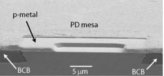
In order to satisfy these requirements, we developed a self-planarization-passivation process using a low-κ dielectric ma-terial called BCB [8]. We spin on and cure a∼10-µm-thick BCB film, creating a glass-like material over the wafer sur-face. The etch-back process, used to planarize the BCB film with the top of the device mesas, is performed using a UHF plasma etcher in two steps. In the steps leading to this etch-back step, the top of the PD mesa was masked with SiO and the EAM waveguides were encapsulated in SiN [see Fig. 8(a)]. The first step in the etch-back process utilizes a specif-ically designed recipe that offers large selectivity between BCB and SiN/SiO. This etch recipe is used to remove the BCB until the first exposure of the top of the SiN-encapsulated EAM ridge waveguides. The second step utilizes a different recipe that pos-sesses only slight selectivity between BCB and SiN/SiO. This step removes BCB and SiN from the top surfaces of the waveg-uides, creating a clean surface forp-metallization of the EAMs. For the EAM, both BCB and the encapsulating SiN layer serve as sidewall passivation materials, while for the PD, only BCB is used. During this step, we focused our attention on properly clearing the BCB-SiN from the EAM waveguides only. Once this step is completed, however, the PD is automatically quasi-planarized with the EAM since we deposited a thick oxide film on top of the mesaareaprior to the PD mesadefinition step. This oxide film is subsequently removed allowing access to the
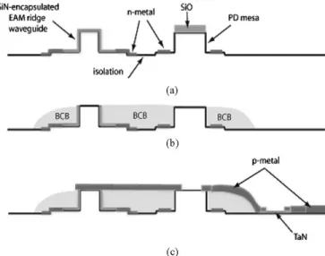
p-region of the PD. Fig. 7 shows a cross section of a planarized
Fig. 8. Illustration of photonic switch cross section after (a) n-contact de-position, (b) BCB planarization, passivation, and patterning, and (c) TaN and p-metal deposition. Note: The features in this illustration are not drawn to scale.
Fig. 9. SEM cross sections of (a) the planarized EAM ridge waveguide and (b) planarized PD-EAM integrated switch.
EAM. Fig. 9(b) is a demagnified cross-sectional picture showing the planarized PD and EAM from one integrated switch along with the interconnectingp-metallization that is deposited in a later step. This technique can be used to planarize and passi-vate a wide variety of semiconductor structures. An extended discussion of this technique can be found in [8].
G. BCB Patterning for Multilevel Interconnect Routing
Once wafer planarization has been achieved, there still ex-ists the additional challenge of routing interconnect metal from one level to another. This could be achieved using vias and plug metallization, however, these techniques are not mature in compound semiconductor processing technology. An alter-native solution is to etch the planarization material such that a slope is created at the interface between two levels where metal interconnection is required. In this way, metal can simply be deposited where needed and travel from one level to another level as required by the circuit architecture.
Fig. 10. SEM cross section showing tapered BCB profile enabling metal in-terconnect to run from topp-contact of PD and EAM to the substrate level.
For the PD-EAM switch integration, in order to have access to then-contact layers of the PD and EAM, to create approxi-mately planar probe contact pads, to provide space for the TaN on-chip resistor, and to clear lines for waveguide cleaving, the BCB must be selectively removed in many places across the sample. We use an SF6/O2-based reactive ion etch (RIE) process
that attacks BCB and photoresist with little selectivity. After the lithography is completed, the photoresist is reflown to provide a tapered thickness near the edges of the photoresist pattern. We perform the RIE step until the substrate is clear of BCB in the unmasked areas. The BCB underneath the tapered photore-sist boundaries also acquires this tapered shape since there is little etch selectivity between the two materials. This creates a sloped BCB region between the top of the BCB and the sub-strate, conveniently allowing smooth multilevel routing of the
p-metalization from the top of the BCB (PD and EAM p-contact
level) to the substrate [see Fig. 8(b)]. Fig. 10 shows a picture of the tapered BCB profile created by the above technique.
H. Other Steps
The other steps in the PD-EAM integration process include standard electron-beam evaporation ofp- a nd n-metals, sputter-ing of TaN [26] for thin film resistor deposition [see Fig. 8(c)], and contact annealing for the formation of ohmic contacts. The wafers are then lapped to a thickness of 120µm, cleaved into 200–300-µm-long bars (along the direction of the EAM waveg-uides), and mounted into a copper fixture.
IV. INTEGRATIONVALIDATION: PROOF-OF-CONCEPT
DEMONSTRATION
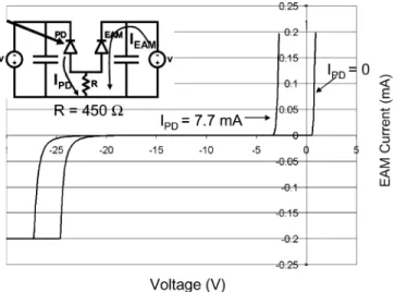
As a successful demonstration of the integration techniques described in the previous section, Fig. 11 demonstrates the fun-damental optoelectronic functionality of the PD-EAM switch shown in Fig. 1. Here we show the EAM current,IEAM ver-sus the EAM supply voltage,VS-EAMin the absence and in the presence of acontinuous-wave beam incident on the PD. By examining the circuit configuration shown in Fig. 1, we find that current from the PD results in a voltage drop across the on-chip integrated TaN resistor. Consequently, the voltage at thep-side of the EAM increases in the presence of photocurrent from the PD, thereby reducing the voltage drop across the EAM. When sweeping the EAM supply voltage in the presence of pho-tocurrent from the PD, a larger reverse bias across the EAM is needed to achieve the same current level than in the absence of
Fig. 11. EAM current as a function of supply voltage forIPD= 0 a nd 5 mA. The shift is 3.6 V.
Fig. 12. 1.25 Gb/s eye diagram of PD-EAM integrated photonic switch op-eration. The data stream incident on the PD has an average power of 5.6 mW at 1552 nm, while the EAM output (shown above) operates at 1556 nm and exhibits greater than 10 dB RF extinction ratio. The PD supply voltage is 15 V, while the EAM supply voltage is 10 V.
photocurrent from the PD. Hence, light shining on the PD, which in turn generates a PD photocurrent, controls the voltage across the EAM. In Fig. 11, we find that in the presence of 7.7 mA of PD current the EAM IV curve is shifted by 3.6 V towards larger reverse biases. This voltage shift is in good agreement with the approximate expected shift of 7.7 mA× 450 Ω, where 450 Ω is the resistance value of the on-chip resistor.
Fig. 12 demonstrates dynamic operation of the PD-EAM in-tegrated photonic switch. In particular, this result shows wave-length conversion from 1552 nm (incident on the PD) to 1556 nm (exiting the EAM) at 1.25 Gb/s. In this case, the PD supply volt-age was 15 V, the EAM supply voltvolt-age was 10 V, and the avervolt-age optical power for the PD was 5.6 mW. The data stream exiting the EAM exhibited an RF extinction ratio greater than 10 dB. The device shown in Fig. 12 was intentionally designed to op-erate at this relatively low switching speed for proof-of-concept purposes and was not limited by any fundamental parasitics introduced by the fabrication techniques discussed in this pa-per. In general, for any PD and EAM wavelengths within the
C-band this switch is capable of high-performance wavelength conversion, data broadcasting, partial optical regeneration, and space switching when operating within a 2-D array of switches. Detailed discussions of the device design and functionality, as well as demonstrations of high-speed operation, can be found elsewhere [5]–[9], [14], [16]–[18].
V. CONCLUSION
In conclusion, we report in this paper a monolithic integration technique that can be utilized to intimately integrate multiple optoelectronic devices in different geometries (waveguide and mesa) with largely different epitaxial layers, all on a single chip. This approach allows for the realization of compact, high-speed integrated photonic circuits on III–V platforms. The important features of this integration method include: 1) the use of multiple selective area regrowths (where completely different epitaxial layers can be grown), 2) the use of selective etch-stop layers (for providing reliable SAG integration and device electrical isolation), 3) the use of a carefully designed sequence of dry and wet etches (which can pattern different geometry devices out of different epitaxial layers), and finally 4) the use of a polymer planarization and passivation process (which provides quasi-planarization in the vicinity of separately grown devices possibly of slightly different height and smooth interconnection surface between them and from their top surfaces to the substrate level).
Here, we demonstrate the use of this multigrowth integration technique for the successful implementation of an integrated photonic switch that incorporates a quantum-well electroab-sorption waveguide modulator and a surface-illuminated mesa photodiode along with electrical components as a part of an on-chip integrated circuit. This integrated device exhibits efficient operation at high speeds due to its compact and low-parasitic implementation using this monolithic integration technique.
REFERENCES
[1] L. A. Coldren, “Widely-tunable chip-scale transmitters and wavelength converters,” Proc. OSA Tech. Dig., Optical Society of America, Integrated
Photonics Research (IPR), Washington, DC, pp. 6–8, 2003.
[2] J. Hutchinson, J.-F. Zheng, J. S. Barton, M. L. Masanovic, M. N. Sysak, J. A. Henness, L. A. Johansson, D. J. Blumenthal, L. A. Coldren, H. V. Demir, V. A. Sabnis, O. Fidaner, J. S. Harris Jr., and D. A. B. Miller, “Indium phosphide based wavelength conversion for high speed optical networks,” Intel Technol. J., vol. 8, no. 2, pp. 161– 171, 2004.
[3] J. W. Raring, E. J. Skogen, L. A. Johansson, M. N. Sysak, S. P. DenBaars, and L. A. Coldren, “Widely tunable negative-chirp SG-DBR laser/EA-modulated transmitter,” J. Lightw. Technol., vol. 23, no. 1, pp. 80–86, Jan. 2005.
[4] K. Takahata, Y. Muramoto, H. Fukano, K. Kato, A. Kozen, O. Nakajima, and Y. Matsuoka, “46.5-GHz-bandwidth monolithic receiver OEIC con-sisting of awaveguide p-i-n photodiode and a HEMT distributed ampli-fier,” IEEE Photon. Technol. Lett., vol. 10, no. 8, pp. 1150–1152, Aug. 1998.
[5] V. A. Sabnis, H. V. Demir, O. Fidaner, J. S. Harris Jr., D. A. B. Miller, J.-F. Zheng, N. Li, T.-C. Wu, H.-T. Chen, and Y.-M. Houng, “Optically-controlled electroabsorption modulators for unconstrained wavelength conversion,” Appl. Phys. Lett., vol. 84, no. 4, pp. 469– 471, 2004.
[6] H. V. Demir, V. A. Sabnis, O. Fidaner, J.-F. Zheng, J. S. Harris Jr., and D. A. B. Miller, “Multifunctional integrated photonic switches,” IEEE Sel.
[7] V. A. Sabnis, H. V. Demir, O. Fidaner, J. S. Harris Jr., D. A. B. Miller, J.-F. Zheng, N. Li, T.-C. Wu, and Y.-M. Houng, “Optically-switched dual-diode electroabsorption modulators,” in Proc. OSA Conf. Integrated
Pho-tonics Research (IPR), OSA Tech. Dig. Opt. Soc. of America, Paper IMB3,
Washington, DC, 2003, pp. 12–14.
[8] H. V. Demir, J.-F. Zheng, V. A. Sabnis, O. Fidaner, J. P. Hanberg, J. S. Harris, Jr., and D. A. B. Miller, “Self-aligning planarization and pas-sivation in the integration of III–V semiconductor devices,” IEEE Trans.
Semicond. Manuf., vol. 18, no. 1, pp. 182–189, Feb. 2005.
[9] J.-F. Zheng, J. P. Hanberg, H. V. Demir, V. A. Sabnis, O. Fidaner, J. S. Harris Jr., and D. A. B. Miller, “Novel passivation and pla-narization in the integration of III–V semiconductor devices,” in Proc.
SPIE Photonics West Conference, Paper 5356-9, San Jose, CA, Jan.
24–29, 2004.
[10] H. Yasaka, M. Okuno, and H. Sugahara, “Device technologies for photonic networks,” NTT Tech. Rev., vol. 1, no. 8, pp. 49–59, 2003.
[11] S. Kodama, T. Ito, N. Watanabe, S. Kondo, H. Takeuchi, H. Ito, and T. Ishibashi, “200 Gbit/s monolithic photodiode-electroabsorption modu-lator optical gate,” in Proc. Device Research Conf. (DRC), Notre Dame, IN, 2001, pp. 151–52.
[12] H. Kitabayashi, Y. Umeda, T. Furuta, N. Watanabe, T. Akeyoshi, Y. Yamane, K. Murata, N. Shimizu, and Y. Ishii, “Monolithic integra-tion technology using InP-based HEMT’s and a uni-traveling-carrier-photodiode for over 40 Gb/s digital OEIC,” in Proc. Int. Conf. Indium
Phosphide Related Materials, Williamsburg, VA, USA, 2000, pp. 329–
332.
[13] U. Eriksson, P. Evaldsson, and K. Streubel, “Fabrication of a 1.55-µm VCSEL and an InGaAsP-InP HBT from a common epitaxial struc-ture,” IEEE Photon. Technol. Lett., vol. 11, no. 4, pp. 403–405, Apr. 1999.
[14] H. V. Demir, V. A. Sabnis, O. Fidaner, J. S. Harris, Jr., D. A. B. Miller, and J.-F. Zheng, “Dual-diode quantum-well modulator for C-band wavelength conversion and broadcasting,” OSA Opt. Express, vol. 12, no. 2, pp. 310– 316, 2004.
[15] D. A. B. Miller, D. S. Chemla, T. C. Damen, A. C. Gossard, W. Wiegmann, T. H. Wood, and C. A. Burrus, “Bandedge electro-absorption in quantum well structures: The quantum confined Stark effect,” Phys. Rev. Lett., vol. 53, pp. 2173–2177, 1984.
[16] H. V. Demir, V. A. Sabnis, J.-F. Zheng, O. Fidaner, J. S. Harris, Jr., and D. A. B. Miller, “Scalable wavelength-converting crossbar switches,” IEEE
Photon. Technol. Lett., vol. 16, no. 10, pp. 2305–2307, Oct. 2004.
[17] O. Fidaner, H. V. Demir, V. A. Sabnis, J. S. Harris, Jr., D. A. B. Miller, and J.-F. Zheng, “Electrically-reconfigurable multifunctional integrated phonic switches,” in Proc. 17th Annu. Meeting IEEE LEOS, Rio Grande, Puerto Rico, vol. 2, Nov. 2004, pp. 455–456.
[18] V. A. Sabnis, H. V. Demir, M. B. Yairi, J. S. Harris, Jr., and D. A. B. Miller, “High-speed, optical switching based on diffusive conduction in an optical waveguide with surface-normal optical control,” J. Appl. Phys., vol. 95, no. 5, pp. 2258–2263, 2004.
[19] T. Van Caenegem, I. Moerman, and P. Demeester, “Selective area growth on planar masked InP substrates by metal organic vapour phase epitaxy (MOVPE),” Progr. Cryst. Growth Characterization, vol. 35, no. 2–4, pp. 263–288, 1997.
[20] M. Ida, N. Shigekawa, T. Furuta, H. Ito, and T. Kobayashi, “Compositional change near the mask edge in selective InGaAs growth by low temperature MOCVD,” J. Cryst. Growth, vol. 158, pp. 437–442, 1996.
[21] L. Silvestre, A. Ougazzaden, D. Delprat, A. Ramdane, C. Daguet, and G. Patriarche, “Study of growth rate and composition variations in met-alorganic vapour phase selective area epitaxy at atmospheric pressure and application to the growth of strained layer DBR lasers,” J. Cryst. Growth, vol. 170, pp. 639–644, 1997.
[22] T. Itagaki, M. Takemi, T. Takiguchi, T. Kimura, Y. Mihashi, and S. Takamiya, “Effects of the mask geometry on the selective-area growth by metalorganic chemical vapor deposition,” in Proc. 22nd Int. Symp.
Compound Semiconductors, 1995, pp. 127–132.
[23] G. B. Stringfellow, Organometallic Vapor-Phase Epitaxy. New York: Academic, 1989.
[24] A. R. Clawson, “Guide to references on III–V semiconductor chemical etching,” Mater. Sci. Eng. R-Rep., vol. 31, pp. 1–438, 2001.
[25] J. Schramm, “Reactive Ion Etching of Indium-Based Compounds Using Methane-Hydrogen-Argon,” Ph.D. dissertation, Univ. Calif., Santa Bar-bara, 1995.
[26] M. L. Lovejoy, G. A. Patrizi, D. J. Rieger, and J. C. Barbour, “Thin-film tantalum-nitride resistor technology for phosphide-based optoelectron-ics,” Thin Solid Films, vol. 290–291, pp. 513–517, 1996.
Vijit A. Sabnis (S’96–M’04) received the B.S. de-gree (highest honors, honors program) in electrical engineering and computer sciences from the Univer-sity of California, Berkeley, in 1995. He received the M.S. and Ph.D. degrees in electrical engineering from Stanford University, Stanford, CA, in 1997 and 2003, respectively. At Stanford University, he studied under Professors James S. Harris, Jr., and David A. B. Miller. His doctoral research was in the areas of epitaxial growth, fabrication, simulation, and char-acterization of optically controlled electroabsorption modulators.
Since 2003, he has been employed at Translucent Incorporated, Palo Alto, CA, where he is investigating new materials for electronic and photonic appli-cations. He has published over 15 journal and conference papers and holds three patents.
Dr. Sabnis is a Member of the Optical Society of America. He received the National Science Foundation Graduate Fellowship from 1996 to 1999.
Hilmi Volkan Demir (S’98–M’04) received the B.Sc. degree in electrical and electronics engineering from Bilkent University, Ankara, Turkey, in 1998. He received the M.S. and Ph.D. degrees in electri-cal engineering from Stanford University, Stanford, CA, in 2000 and 2004, respectively. At Stanford Uni-versity, his doctoral research under Professors David A. B. Miller and James S. Harris, Jr., focused on invention, design, fabrication, testing, and modeling of multifunctional integrated photonic switches; his Ph.D. dissertation led to the world’s first wavelength-converting crossbar switches.
In September 2004, he joined Bilkent University, where he is currently As-sistant Professor of Physics. He is also Associate Director of Bilkent Nanotech-nology Research Center and a Faculty Member of Bilkent Advanced Research Laboratory. He has published more than 20 journal and conference papers, pre-sented more than ten invited talks, co-translated two books, and disclosed four U.S. patents (two granted, one filed, one in continuation).
Dr. Demir is a recipient of the Stanford Intel Research Assistantship (2000– 2004), the Edward L. Ginzton Fellowship (1998–1999), and the Bilkent Board of Trustees Scholarship (1994–1998). He was one of the Stanford–Berkeley Innovator’s Challenge Finalists, in 2003, and an invited participant of London International Youth Science Forum, London, U.K., in 1994.
Onur Fidaner (S’00) received the B.Sc. degree in electrical and electronics engineering from Middle East Technical University (METU), Ankara, Turkey, in 2001 and the M.S. degree in electrical engineering from Stanford University, Stanford, CA, in 2003. He is a Lucent Technologies Stanford Graduate Fellow-ship Student at Stanford University and he is currently working toward the Ph.D. degree in electrical engi-neering under Prof. David A. B. Miller.
His research involves investigating new integrated multifunctional photonic devices with quantum well structures on both III–V semiconductors and silicon.
Jun-Fei Zheng received the Ph.D. degree in materi-als science from University of California, Berkeley, in 1994.
Since then, he has been with Intel Corporation working on silicon process technology development, advanced MOS transistors, and photonic and opto-electronic devices. He was with Intel Strategic Tech-nology Group and an Intel Researcher-in-Residence at Stanford University from 2001 to 2004. Currently, he is a Senior Staff Scientist at Intel Strategic Tech-nology Group and an Intel Visiting Fellow at Yale University, New Haven, CT.
James S. Harris (F’88) received the B.S., M.S., and Ph.D. degrees in electrical engineering from Stanford University, Stanford, CA, in 1964, 1965, and 1969, respectively.
He is the James and Ellenor Chesebrough Profes-sor of Engineering at Stanford University. In 1969, he joined the Rockwell International Science Center, Thousand Oaks, CA, where he was one of the key contributors in developing their preeminent position in GaAs device technology. In 1982, he joined the Solid State Electronics Laboratory, Stanford Univer-sity, as Professor of Electrical Engineering. He served as the Director of the Solid State Electronics Laboratory at Stanford University from 1981 to 1988. His cur-rent research interests are in the physics and application of ultrasmall structures to new electronic and optoelectronic devices and high-speed integrated circuits and MBE growth coupled with a scanning-probed-induced oxidation for fabri-cation of nano three-dimensional structures. He has more than 500 publifabri-cations in these areas.
Dr. Harris, Jr., is a Fellow of the American Physical Society and he received the Heinrich Walker Medal, IEEE Third Millenium Medal, and the 2000 IEEE Morris N. Liebmann Memorial Award for his contributions to GaAs devices and technology.
David A. B. Miller (M’84–SM’89–F’95) received the B.Sc. degree from St. Andrews University, St. Andrews, U.K., and the Ph.D. degree from Heriot-Watt University, Edinburgh, U.K., in 1979.
From 1981 to 1996, he was with Bell Laborato-ries, and from 1987, as a department head, formerly of the Advanced Photonics Research Department. Cur-rently, he is the W. M. Keck Professor of Electrical Engineering at Stanford University, Stanford, CA, and the Director of the Ginzton and Solid State and Photonics Laboratories, Stanford, CA. His research interests include quantum-well optoelectronic and nanophotonic physics and devices, and fundamental and applications of optics in information, sensing, switching, and processing. He has published more than 200 scientific papers, and holds over 55 patents.
Dr. Miller has served as a Board member for both the Optical Society of America (OSA) and IEEE Lasers and Electro-Optics Society (LEOS), and in various other society and conference committees. He was President of the IEEE Lasers and Electro-Optics Society in 1995. He was awarded the Adolph Lomb Medal and the R. W. Wood Prize from the OSA, the International Prize in Optics from the International Commission for Optics, and the IEEE Third Millennium Medal. He is a Fellow of the Royal Societies of London and Edinburgh, OSA, and the American Physics Society (APS), and holds honorary degree from the Vrije Universiteit Brussel and Heriot-Watt University.
Nelson Li, photograph and biography not available at the time of publication.
Ta-Chung Wu, photograph and biography not available at the time of publication.
H.-T.Chen, photograph and biography not available at the time of publication.
Yu-Min Houng, photograph and biography not available at the time of publication.
![Fig. 1. Circuit diagram and principle of operation of PD-EAM photonic inte- inte-grated circuit [6].](https://thumb-eu.123doks.com/thumbv2/9libnet/5838357.119636/2.918.102.429.101.276/fig-circuit-diagram-principle-operation-photonic-grated-circuit.webp)