1Abstract—In this paper a high-performance low-voltage
low-power CMOS second-generation current conveyor (CCII) is presented. The proposed CCII is based on super transistor (ST) and enables low input impedance at X terminal and high output impedance at Z terminal. It also utilizes a novel power saving strategy in which a single NMOS cascode current mirror conveys X terminal current to Z terminal, provides high impedance at Z terminal and reduces the X terminal impedance all together resulting in a low-power and compact structure. As another advantage, only NMOS transistors are used in processing voltage and current signals granting the proposed CCII high frequency operation. PMOS transistors are used only for biasing. However, the proposed CCII cannot provide infinite impedance at Y terminal. HSPICE simulations using 0.18 µm parameters and supply voltage of ±0.9 V confirms that the proposed CCII exhibits impedances of 0.155 Ω, 1.6 MΩ and 47 kΩ at X, Z and Y terminals, respectively. Voltage and current bandwidths are also 377 MHz and 159 MHz, respectively. Some of the applications of the proposed CCII are given.
Index Terms—Current-mode circuits; Analog integrated circuits.
I. INTRODUCTION
In the last decade, current-mode (CM) signal processing has become very popular [1]–[20]. It provides innovative solutions to solve the problems of analog circuits in modern technologies and shows many advantages compared to conventional voltage-mode (VM) approach. Especially, current-mode technique allows realizing low-voltage, wide dynamic range and large bandwidth analog circuits and alleviates the problems of constant gain bandwidth product [1]–[20].
One of the most important current-mode building blocks is second-generation current conveyor (CCII) (Fig. 1) which finds many applications in implementing filters, instrumentation amplifiers, voltage and current amplifiers, oscillators etc. [3]–[14]. Moreover, having one high impedance input, one low impedance input and one high impedance output, it can operate in both current and voltage modes, which provides flexibility and enables variety of circuit designs.
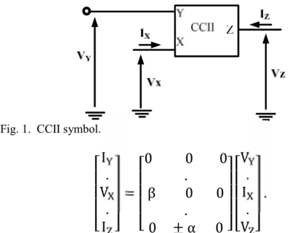
The voltage applied to terminal Y of CCII is replicated to its X terminal. The current supplied to X terminal is conveyed to the high impedance output terminal Z with
Manuscript received 3 September, 2017; accepted 22 January, 2018.
either positive (CCII+) or negative polarities (CCII-). Therefore, X and Y terminals exhibit very low (ideally zero) and very high (ideally infinite) impedances, respectively. However non-ideal impedances at X and Z terminals and other parasitic elements limit the performance of CCII [19]. Furthermore, CCII’s frequency performance directly determines the frequency performance of all circuits implemented with CCIIs. Consequently, a high-performance CCII (with high bandwidth, very low impedance at X terminal and very high impedance at Z terminal) are needed to improve the performance of CCII based circuits. However, the demand for low-voltage low-power operation [21] makes the design of such a high performance CCII very challenging.
Fig. 1. CCII symbol.
⎣ ⎢ ⎢ ⎢ ⎡I. V . I ⎦⎥ ⎥ ⎥ ⎤ = ⎣ ⎢ ⎢ ⎢ ⎡0 .0 0 β 0 0 . 0 ± α 0 ⎦⎥ ⎥ ⎥ ⎤ ⎣ ⎢ ⎢ ⎢ ⎡V. I . V ⎦⎥ ⎥ ⎥ ⎤ . (1)
Literature survey shows that the previously reported CCIIs are mainly based on differential pair/transconductance and translinear topologies [3]–[4], [14], [15], [18], [22], [23]. In CCIIs made of differential pairs, a high gain negative feedback loop is used to reduce impedance at X terminal. In this approach, low impedance at X terminal, infinite impedance at Y terminal and wide frequency bandwidths (for both voltage and current signals) are achieved. However most of the CCIIs made of differential pair (or transconductance amplifier) topologies suffer from low impedance at Z terminal [3], [4], [12], [22]. Most importantly the impedance at X terminal starts to increase at frequencies much lower than voltage and current bandwidths. On the other hand, CCIIs based on translinear topology are not suitable for low voltage designs because they require large supply voltage of at least 2V + 2V (with usual meaning of symbols) [15] and low impedance at
A Novel Super Transistor-Based
High-Performance CCII and Its Applications
Leila Safari
1, Shahram Minaei
21
Independent Researcher,
Tehran, Iran
2
Department of Electronics and Communications Engineering, Dogus University,
Acibadem, Istanbul, Turkey
X terminal is achievable at the cost of high power consumption. In addition, they suffer from low impedance at Z terminal and poor frequency performance because both P-type and N-P-type current mirrors are present in the signal path.
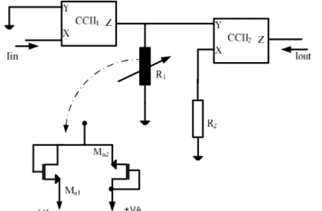
In this paper, a new topology to design high-performance CCII is proposed. The proposed topology is based on super transistor (ST) and enables very low input impedance and very low offset voltage at X terminal and high output impedance at Z terminal. Unlike differential pair topology, impedance at X terminal remains low even at high frequencies. The proposed topology includes an interesting power saving strategy in which a single NMOS cascode current mirror serves three functions simultaneously; it conveys X terminal current to Z output, provides high impedance at Z terminal and helps further reducing the X terminal impedance by establishing a negative feedback loop. Consequently, the proposed CCII enjoys a compact structure. As another advantage, only NMOS transistors are used in processing voltage and current signals granting the proposed CCII high frequency operation. However, similar to translinear based CCIIs, its impedance at Y terminal is not infinite. As application examples, the proposed CCII, is used in implementing a current-mode instrumentation amplifier, an electronically variable voltage amplifier and an electronically variable current amplifier. This paper is organized as follows: In Section II the proposed CCII circuit and its HSPICE simulation results using 0.18 µm TSMC CMOS technology are presented. Thereafter, CCII applications are discussed in Section III. The paper is concluded in Section IV.
II. THEPROPOSEDCCII A. Circuit Description
The proposed topology is based on STs which have been used in voltage-mode signal processing to improve the output resistance and linearity of source-degenerated differential CMOS transconductors [24]. In current-mode signal processing, they have been used to design a high-performance voltage feedback current amplifier [2].
The implementation and symbol of a ST is shown in Fig. 2. It has three interesting characteristics making them highly suitable to design other current-mode building blocks especially CCIIs:
First, they exhibit very low input impedance at source terminal expressed as [24]
r ≈ ( ‖ )( ‖ ). (2)
Second, they show high voltage tracking accuracy between gate and source terminals. Voltage gain between source and gate terminals is expressed as [24]
A = ≈ [ ( ‖ ) ( ‖ )] ≈ 1. (3)
Third, the output impedance seen from their drain is very high and is described by [24]
r g g g (R)(r ‖r )(r ‖r )(r ), (4)
where R is the equivalent resistance connected to the source node. In (2)–(4) gmand rodenote the transconductance and output impedance of the related transistor or current source, respectively.
Fig 2. Implementation and symbol of Super Transistor [24].
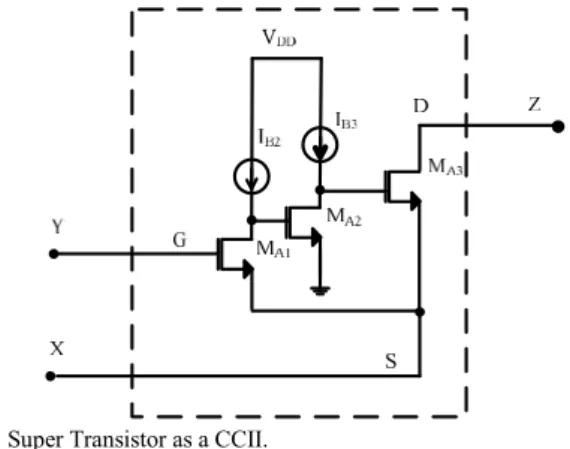
For typical parameter values; rs, Avand rdare in Ω, unity and GΩ ranges, respectively. These interesting features lead us to consider a single super transistor as a high performance CCII as is shown in Fig. 3 which has very low impedance at X terminal, close to unity gain between Y and X terminals and very high output impedance at Z terminal. Despite the intrinsic capacity of STs to operate as a CCII, up to now, they have not been employed in the structure of current conveyors. Here for the first time, we employ ST as the core part of a high performance CCII.
Fig 3. Super Transistor as a CCII.
As it is seen from Fig. 3, there is a DC level shift equal to VGSMA1 between Y and X terminals. Transistor MA3 also requires DC bias current. Therefore, some modifications in Fig. 3 are needed to make it a high performance CCII. Fig. 4 shows the simplified schematic of the proposed CCII which is made up of only 8 NMOS transistors (excluding bias circuitry). Transistor M1which is identical to MA1is used to reduce DC offset voltage between Y and X terminals. For DC input, a simple analysis shows that gate voltage of M1 and VXcan be expressed as:
V = V + V , (5)
V = V − V = V + V − V . (6)
Therefore, for VY= 0, offset voltage can be found as
V = V − V = V = V − V , (7)
V ≈ × ( V − V ). (8) Evidently, low offset voltage can be achieved by making VDSMA1as close as possible to VDSM1.
In Fig. 4 current sources IB2 and IB3 should be equal to provide matching between M1and MA1. In addition, current sources IB1 and IB2 should also be equal because any difference between IB1 and IB2 will appear as an offset current at Y terminal.
Fig. 4. Simplified schematic of the proposed CCII.
By performing a simple small-signal analysis and using (3), voltage transfer between Y and X terminals can be expressed as (Appendix-B)
≈ m1 oIB2
m1 oIB2≈1, (9)
where gmi and roIBi are transconductance and output resistance of related transistor and current source, respectively.
If we neglect the effect of negative feedback established by M2–M5and only consider the effect of super transistor, the impedance at X terminal can be expressed as (2) (by replacing r and r with r and r , respectively). However, if a single transistor (gmA1) is used instead of super-transistor, the impedance at X terminal will be
r′ ≈ . (10)
Considering (9) and comparing (2) and (10), shows that innovative use of super transistor not only increases the voltage transfer accuracy between X and Y terminals, but it results in a significant reduction in X terminal impedance.
Cascode current mirror formed by transistors M2–M5 serves three vital functions:
First; it duplicates the current in the X terminal to the Z output (assuming that IB3+ IB5= IB6).
Second; it provides high impedance at Z terminal. Third; it forms a negative feedback loop that further reduces the impedance at X terminal.
As it can be seen, several important features are provided by only 4 transistors resulting in low power consumption, compact and easy to design structure.
By considering the effect of negative feedback formed by M2–M5transistors and using (2), the overall impedance at X terminal is found as:
r′ ≈ ( ‖ )( ‖ ) . (11)
From (11), it is evident that the proposed CCII enjoys very low impedance at X terminal.
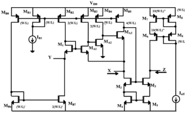
Complete schematic of the proposed CCII is shown in Fig. 5 in which ideal current sources are implemented by simple current mirrors made of transistors MB0–MB7. Besides, transistors M6–M9and current source Ioffare used to provide DC current for M2-M5 transistors. Cascode structures made of transistors M2–M5 and M6–M9 at the output branch are used to increase impedance at Z terminal. Analysing circuit of Fig. 5, the impedance at Z terminal is found as
R (g r r )‖(g r r ). (12)
The impedance at Y terminal is also found as
R r ‖(g + r ). (13)
As it is seen from (13), the impedance at Y terminal is not infinite. Limited impedance at Y terminal can only cause a negligible reduction in β value of CCII. By considering RY, the amount of reduction will be
= , (14)
where RS is the internal impedance of voltage source connected to Y terminal. As RSis in ohm range, and RYis in kohm range, therefore, K ≈ 1 and the limited impedance will not have a serious effect on CCII’s performance. However, if larger impedances at Y terminal is required, simple current mirrors used for biasing, can be replaced with high output impedance cascode type current mirrors.
Fig. 5. Complete schematic of the proposed CCII. B. Simulation Results
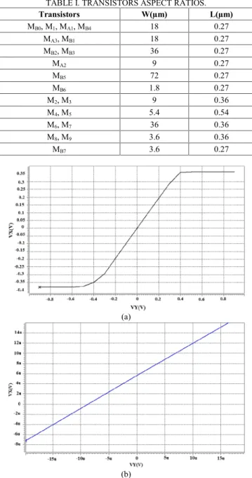
Performance of the proposed circuit of Fig. 5 is verified by HSPICE simulations using 0.18 µm TSMC CMOS process parameters under supply voltage of ±0.9 V. Transistors aspect ratios are reported in TABLE I. According to the transistors aspect ratios shown in Fig. 5, to satisfy IZ= IXwe should have 10 Ioff= 6 IB1. The values of IB1 and Ioff are set at 15 µA and 9 µA respectively. A compensation capacitor of 0.4 pF is also added between gate and drain of MA3for frequency compensation.
DC transfer characteristic of X terminal voltage (VX) against input voltage at terminal Y (VY) (shown in Fig. 6) is achieved while Z terminal is connected to ground. Figure 6(a) shows that maximum and minimum voltage limits at terminal X are 350 mV and −350 mV, respectively. Figure 6(b) shows that DC offset voltage at X terminal for VY=0 is also negligible value of 5.6 µV.
Figure 7 shows error voltage between X and Y terminals for different values of VY. Favourably, error voltage between X and Y voltage remains below 25 mV. In Fig. 8 an input sinusoidal voltage having amplitude of 100 mV and frequency of 100 kHz, is applied to Y node, and the resulting signal on X-terminal is observed. THD is only 0.31 %. By increasing frequency, the value of THD reaches to 0.23 % and 0.21 % at 1 MHz and 10 MHz, respectively.
TABLE I. TRANSISTORS ASPECT RATIOS.
Transistors W(µm) L(µm) MB0, M1, MA1, MB4 18 0.27 MA3, MB1 18 0.27 MB2, MB3 36 0.27 MA2 9 0.27 MB5 72 0.27 MB6 1.8 0.27 M2, M3 9 0.36 M4, M5 5.4 0.54 M6, M7 36 0.36 M8, M9 3.6 0.36 MB7 3.6 0.27 (a) (b)
Fig. 6. VXversus VYchanging from a) -0.9 V to +0.9 V b) around 0 V.
The change in the Z terminal output current against the X terminal input current is also shown in Fig. 9 in which IXis changed from −85 µA to +85 µA. Favourably, the input impedance at X terminal is 0.155 Ω which is very close to the ideal value of zero. Such low input impedance at X terminal is a direct result of using super transistor according
to (11). The impedance at Z and Y terminals are 1.6 MΩ and 47 kΩ, respectively. Total power dissipation is also 0.451 mW.
Fig. 7. Voltage Error between VXand VY.
Fig. 8. VXand VYin time domain.
Fig. 9. IZversus IX.
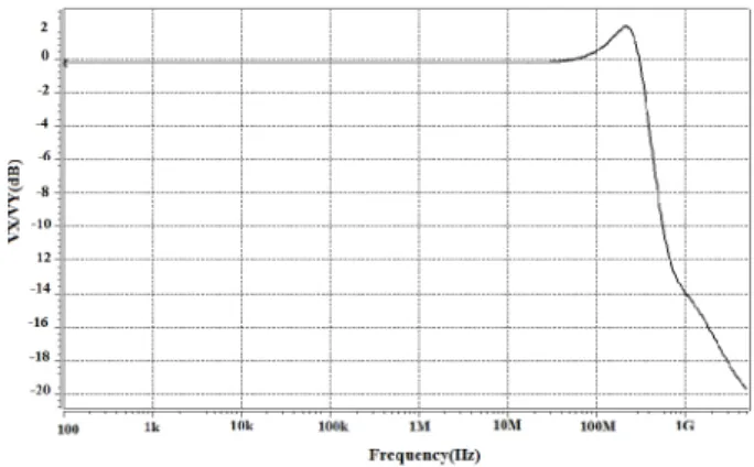
The frequency response of (VX/VY) is shown in Fig. 10 where, VYis the AC signal, X terminal is open circuited and Z terminal is grounded. The proposed CCII has a wide voltage gain -3 dB bandwidth of 377 MHz with a gain of 0.969. As it is seen, the voltage transfer response shows a peak of 2 dB. If a flat response is required, the value of compensation capacitor should be increased to 1 pF, however it will result in degradation in frequency performance. Figure 11 shows the frequency response of Iz versus IXwhere, Y and Z terminals are connected to ground and AC current signal is applied to X terminal. The proposed CCII exhibits a current gain -3 dB bandwidth of 195 MHz and current transfer gain of 0.965. The resulted high frequency performance is due to the fact that only NMOS transistors are used in processing voltage and current signals. In addition, they are all included in negative feedback loop which further improves frequency performance.
Fig. 10. Frequency response of voltage transfer gain.
Fig. 11. Frequency response of current transfer gain.
Overall characteristic of the proposed CCII is compared with previously reported works in Table II. As it is seen, although CCII of [3] exhibits impedance of less than 7 Ω at X terminal, but it suffers from low voltage and current bandwidths of 10.5 MHz and 6.2 MHz, respectively. The CCII of [4] enjoys high voltage and current bandwidths but it exhibits low impedance of 147 kΩ at Z terminal and consumes 1.3 mW. The low power CCII of [12] exhibits wide voltage bandwidth of 10 GHz, but its current bandwidth is only 32 MHz. The CCII of [15], exhibits moderate frequency performance, consumes high power consumption and exhibits high impedance of 47 Ω at X terminal. The CCII of [18] also exhibits Rx value of 11.4 Ω, poor frequency performance of 16 MHz and requires high supply voltage of ±1.5 V. The proposed CCII exhibits very low impedance at X terminal which is at least 45 times smaller than that of [3], [4], [12], [15], [18], [22], [23]. Its offset voltage at X terminal is only 5.6 µV which is the smallest one in Table II. Its output impedance is 1.6 MΩ and comparable to [15] but much larger than [4]. The output impedance is high enough to enable easy cascading, however it can further be improved by utilizing another ST at output branch. The proposed CCII’s power consumption is two times larger than those of [3], [12], [18] but much smaller than [4], [15]. Compared to [22], [23], the proposed CCII has better frequency performance and lower input (X terminal) impedance. As it is seen in Table II, the proposed CCII has not very high impedance at Y terminal but as it will be shown, this property will not cause any problem in most of the applications.
III. APPLICATIONS OF THEPROPOSEDCCII
In this section, applications of the proposed CCII as an instrumentation amplifier, a variable-gain voltage amplifier
and a variable gain current amplifier are given. In all of these applications the advantage of using high performance CCII is obvious.
A. Instrumentation Amplifier
Figure 12 shows the application of the proposed CCII to implement instrumentation amplifier of [9]. If both CCIIs are well matched and have precise voltage tracking between their Y and X terminals, high common-mode rejection ratio (CMRR) is provided. Unlike conventional voltage-mode instrumentation amplifiers, this circuit does not rely on any external resistor matching to achieve high CMRR, however ultimate limit on CMRR is determined by the mismatch between CCII1 and CCII2. The differential-mode voltage gain and output impedance can be described as:
= ( − ) ‖ ,(15)
R = R , (16)
where Rx3 is the x-terminal impedance of CCII3, RY1, RY2 and RY3are impedances at Y terminal of CCII1, CCII2and CCII3, respectively, and RS1 and RS2 are the internal impedances of voltage sources Vin+and Vin-, respectively. As RY3>> R2, RY1>> RS1, RY2>> RS2, Rx1and Rx2<< R1, and α, β ≈ 1, (15) can be expressed as
≅ . (17)
In order to verify the performance of the instrumentation amplifier of Fig. 12, R1is set to 0.1 kΩ, while R2is varied from 0.1 kΩ to 5 kΩ. Figure 13 shows that while DC differential gain varies from 0 dB to 33 dB, -3 dB bandwidth varies only from 67 MHz (for gain of 0 dB) to 53 MHz (for gain of 33 dB). The -3 dB bandwidth proves to be approximately constant at high frequency for different gain values.
CMRR frequency performance is also shown in Fig. 14. As it can be seen, the instrumentation amplifier of Fig. 12 exhibits CMRR of 83 dB with -3 dB bandwidth of 613 kHz for different values of R2.
Y XCCII1 Vin+ Z X YCCII2 Vin-Z R1 R2 Y XCCII3 Z Vout
Fig. 12. Application of the proposed CCII as instrumentation amplifier [9]. For instrumentation amplifier application, using the proposed CCII results in three major improvements:
1. High CMRR because of the proposed CCII's high accuracy in transferring input signals from Y terminal to X terminal which is achieved because of the used super transistor.
2. Very low output impedance of 0.155 Ω because of very low impedance at X terminal which is achieved because of the used super transistor and negative feedback loop. 3. High frequency performance due to the high frequency performance of the proposed CCII.
TABLE II. COMPARISON BETWEEN PROPOSED CCII AND OTHER RECENT WORKS. Parameters [3] [4] [12]* [15] [18] [21] [22] Proposed Rx(Ω) <7 9.6 15 42 11.4 200 27 0.155 Rz (MΩ) NA 0.147 NA 2.24 7.2 0.560 0.89 1.6 RY ∞ ∞ ∞ 147 kΩ ∞ ∞ ∞ 47 kΩ Vx/Vy BW(MHz) 10.5 810 10000 87 16 99 14 377 Iz/Iy BW(MHz) 6.2 915 32 70 NA 94 13 195 Offset voltage at X(mV) <2.5 0.8 NA 0.2 NA NA NA 0.0056 PD(mW) 0.213 1.3 0.234 2.24 0.210 1.5 0.064 0.451 Technology (µm) 0.35 0.35 0.5 0.8 0.35 0.13 0.18 0.18
Input Voltage dynamic range (mV) ±650 (-1.43)-(+1.1) (-0.63)-(+0.34) NA (-1)-(+0.9) 1.5 ±380 ±350
Input current dynamic range (µA) ±1000 ±3000 ±100 NA NA** NA ±7 ±80
No. of transistors 22 20 14 28 21 25 36 21
Supply Voltage (V) ±0.75 ±1.65 ±1.5 3.3 ±1.5 1.5 ±0.4 ±0.9
Note: *low power wide band version, ** Not Available.
Fig. 13. Frequency response of Differential-Gain of Fig. 12 for R1 = 0.1 kΩ and different values of R2.
Fig. 14. Frequency response of CMRR for R1= 0.1 kΩ and different values of R2.
B. Variable Gain Voltage Amplifier
Figure 15 shows a variable-gain voltage amplifier implemented by the proposed CCII. The input voltage applied to Y1terminal is transferred to X1terminal, where it is translated to current by R1. The output voltage and output impedance can be simply derived as:
A = = ∝ ‖ ≈ , (18)
R = R , (19)
where Rx2is the X terminal impedance of CCII2. To have electronic control, a variable resistor [17] is used as R1. Therefore, the value of voltage gain can be set by control voltages VA and –VA resulting in a high-performance electronically tunable voltage amplifier.
Figure 16 shows the frequency performance of the proposed voltage amplifier. As it can be seen from Fig. 16,
3 dB bandwidth of the proposed voltage amplifier varies between 97 MHz to 85 MHz for different voltage gains from 10 dB to 28 dB respectively. It also exhibits very low output impedance of only 0.155 Ω.
Fig. 15. Application of the proposed CCII as a high-performance variable-gain wide-bandwidth voltage amplifier.
Fig. 16. Gain frequency response of the voltage amplifier of Fig. 15. Using the proposed CCII in voltage amplifier application results in two major improvements:
1. Low output impedance equal to the X terminal impedance of the proposed CCII.
2. Very wide bandwidth as a result of the proposed CCII's high-frequency performance.
C. Variable Gain Current Amplifier
A CCII based variable-gain current amplifier is shown in Fig. 17. In current amplifier of Fig. 17, the input current applied to the low impedance X1 terminal is transferred to the Z1terminal, where it is translated to voltage by R1. The voltage produced at Z1terminal is copied to the X2terminal where it is converted again to current by R2. The current
produced at R2is copied to output terminal (Z2). The current gain, output and input impedances can be simply derived as:
A = =∝ ∝ ‖ ≈ , (18)
R = R , (19)
R = R , (20)
where Rz2is the Z terminal impedance of CCII2. A variable resistor [17] is used as R1 to provide electronic tuning capability for the proposed CCII-based current amplifier. In Fig. 17, current gain can be tuned by control voltages VA and –VA.
Fig. 17. Application of the proposed CCII as a high-performance variable-gain wide bandwidth current amplifier.
Figure 18 shows the frequency performance of the current amplifier of Fig. 17. Interestingly, for R2 = 100 Ω and different values of VA, 3 dB bandwidth of the proposed current amplifier varies between 81.1 MHz to 90 MHz for different current gains ranging from 10.6 dB to 19 dB, respectively. The input and output impedances are also 0.155 Ω and 1.6 MΩ respectively.
Fig. 18. Gain frequency performance of the current amplifier of Fig. 17. Using the proposed CCII in current amplifier application results in two major improvements:
1. Low input impedance equal to the X terminal impedance of the proposed CCII and high output impedance equal to Z terminal impedance of the proposed CCII.
2. Very wide bandwidth as a result of the proposed CCII's high frequency performance.
IV. CONCLUSIONS
A new super transistor-based CCII for low-voltage high frequency applications, has been designed. The proposed
CCII can operate at low supply voltage and exhibits very low impedance at its X terminal. It also exhibits wide frequency performance for both voltage and current transferring. As other merit, the proposed topology exhibits an extremely low offset voltage at X node, therefore, the need for any offset voltage cancellation circuit is alleviated resulting in a very simple structure. The performance of the proposed CCII in applications such as instrumentation amplifier, variable-gain voltage amplifier and variable-gain current amplifier has been tested. The achieved results prove that the proposed CCII is highly suitable for wideband low-voltage low-power applications.
REFERENCES
[1] A. S. Sedra, K. C. Smith, “A second-generation current-conveyor and its applications”, IEEE Trans. Circuit Theory, vol. 17, no. 1, pp. 132– 134, 1970. DOI: 10.1109/TCT. 1970.1083067.
[2] L. Safari, J. Azhari, “A novel wide band super transistor based voltage feedback current amplifier”, International Journal of
Electronics and Communications, vol. 67, no. 7, pp. 624–631, 2013. DOI: 10.1016/j.aeue.2013.01.005.
[3] A. H. Madian, M. Soliman, A. M. Soliman, “New 1.5-V CMOS second generation current conveyor based on wide range transconductor”, Analog Integrated Circuits and Signal Processing, vol. 49, pp. 267–279, 2006. DOI: 10.1007/s10470-006-9703-3. [4] E. Arslan, S. Minaei, A. Morgul, “On the realization of high
performance current conveyors and their applications”, Journal of
Circuits, Systems and Computers, vol. 22, 2013. DOI: 10.1142/S0218126613500151.
[5] K. Gosh, B. N. Ray, “CCII based nth order current mode filter with grounded R and C”, International Journal of Electronics Letters, vol. 3, pp. 105–121, 2013. DOI: 10.1080/21681724.2014.911366. [6] T. Ettaghzouti, N. Hassan, K. Besbes, “Transformation of voltage
mode filter circuit based on op-amp circuit based on CCII”, Journal of
Electronic Science and Technology, vol. 13, pp. 60–67, 2015. [7] E. Yuce, S. Minaei, “New CCII-based versatile structure for realizing
PID controller and instrumentation amplifier”, Microelectronics
Journal, vol. 41, pp. 311–316, 2010. DOI: 10.1016/j.mejo.2010.03. 008.
[8] A. A. Khan, M. A. Al-Turaigi, M. A. El-Ela, “An improved current-mode instrumentation amplifier with bandwidth independent of gain”,
IEEE Trans. Instrumentation Measurement, vol. 44, no. 4, pp. 887– 891, 1995. DOI: 10.1109/19.392876.
[9] C. Toumazou, F. G. Lidgey, “Novel current mode instrumentation amplifier”, Electronics Letters, vol. 25, no. 3, pp. 228–230, 1989. DOI: 10.1049/el:19890163.
[10] T. Kaulberg, “A CMOS current-mode operational amplifier”,
Eighteenth European Solid-State Circuits Conference (ESSCIRC 1992),1992. DOI: 10.1109/ESSCIRC. 1992.5468207.
[11] A. M. Soliman, “Current Mode Oscillators using single output current conveyors”, Microelectronics Journal, vol. 29, no. 11, pp. 907–912, 1998. DOI: 10.1016/S0026-2692(98)00053-6.
[12] W. S. Hassanein, I. A. Awad, A. M. Soliman, “New wide band low power CMOS current conveyors”, Analog Integrated Circuits and
Signal Processing, vol. 40, no. 1, pp. 91–97, 2004. DOI: 10.1023/B:ALOG.0000031439.62496.f9.
[13] L. Grigorescu, “Amplifiers built with current-conveyors”, Journal of
Applied Physics-Instruments, vol. 53, pp. 109–113, 2008.
[14] S. S. Rajput, S. S. Jamuar, “Low voltage low power and high performance current conveyors for low voltage analog and mixed mode signal processing applications”, Analog integrated Circuits and
Signal Processing, vol. 41, no. 1, pp. 21–34, 2004. DOI: 10.1023/B:ALOG.0000038280.45676.e0.
[15] B. Calvo, S. Celma, P. A. Martinez, M. T. Sanz, “High-speed high-precision CMOS current conveyor”, Analog Integrated Circuits and
Signal Processing, vol. 36, no. 3, pp. 235–238, 2003. DOI: 10.1023/A:1024770405352.
[16] A. Naik, N. M. Devashrayee, “Two novel long-tail pair based second generation current conveyors (CCII)”, Information Technology and
Mobile Communication, vol. 147, pp. 95–99, 2011. DOI: 0.1007/978-3-642-20573-6_15.
[17] L. Safari, S. Minaei, E. Yuce, “A new transresistance mode instrumentation amplifier with low number of MOS transistors and Electronic tuning opportunity”, Journal of Circuits systems and
computers, vol. 25, no. 4, 2016. DOI: 10.1142/S0218126616500225. [18] G. Ferri, V. Stornelli, M. Fragnoli, “An integrated improved CCII
topology for resistive sensor application”, Analog Integrated Circuits
and Signal Processing, vol. 48, pp. 247–250, 2006. DOI: 10.1007/s10470-006-7415-3.
[19] A. Fabre, O. Saaid, H. Barthelemy, “On the frequency limitations of the circuits based on second generation current conveyors”, Analog
Integrated Circuits and Signal Processing, vol. 7, pp. 113–129, 1995. DOI: 10.1007/BF01239166.
[20] H. Jia, Y. L, “Design of a novel wideband op amp with CCII structure”, Analog Integrated Circuits and Signal Processing, vol. 85, pp. 445–449, 2015. DOI: 10.1007/s10470-015-0611-2.
[21] X. Zhao, H. Fang, J. Xu, “DC gain Enhancement method for recycling folded cascode amplifiers in deep submicron technology”,
IEICE Electronics Express, vol. 8, no. 17, pp. 1450–1454, 2011. DOI: 10.1587/elex.8.1450.
[22] A. Redan, M. Ibrahim, F. Farag, “Input–output Rail-to-Rail CMOS CCII for low voltage–low power applications”, Microelectronics
Journal, vol. 48, pp. 60–75, 2016. DOI: 10.1016/j.mejo.2015.12.001. [23] M. Kumngern, F. Khateb, “0.5-VBulk-driven second generation
current conveyor”, in Proc. IEEE Symposium on Computer
Applications and Industrial Electronics (ISCAIE 2014), Penang, Malaysia, 2014, pp. 1–2. DOI: 10.1109/ISCAIE.2014.7010233. [24] J. M. Martinez-Heredia, A. Torralba, “Enhanced source-degenerated
CMOS differential transconductor”, Microelectronics Journal, vol. 42, no. 2, pp. 396–402, 2011. DOI: 10.1016/j.mejo.2010.10.011.
APPENDIXA For VGSM1and VGSMA1we have:
V = 1 I 2 μ C WL (1 + λV ) + V ≈ ≈ K 1 − + V , (A.1) ≈ K 1 − + V . (A.2) In which: K = , (A.3) K = . (A.4)
For K1=K2 = K and VthM1 = VthMA1 (assuming identical transistors), by inserting (A.1) and (A.2) into (7), offset voltage is found as V ≈ ( V − V ). (A.5) APPENDIXB V V = g r 1 + g r × × 1 1 + [g (r ‖r )g (r ‖r )] ≈
≈
≈
1, (B.1)where gmi and roIBi are transconductance and output resistance of related transistor and current source, respectively.