www.advmat.de
Near-Unity Emitting Copper-Doped Colloidal Semiconductor
Quantum Wells for Luminescent Solar Concentrators
Manoj Sharma, Kivanc Gungor, Aydan Yeltik, Murat Olutas, Burak Guzelturk,
Yusuf Kelestemur, Talha Erdem, Savas Delikanli, James R. McBride,
and Hilmi Volkan Demir*
DOI: 10.1002/adma.201700821
illumination, the fluorophore's emission is guided and concentrated toward the edge of the slab waveguide through total internal reflection. This emission is then collected and converted to electricity by photovoltaic (PV) cells placed at the thin edges of the waveguide, thus allowing for large-area solar light harvesting with small-area PVs.[3,4] Therefore, LSCs are promising candidates for lowering the solar energy costs by increasing the inci-dent radiation flux with large area of the LSCs exposed to the sunlight, which in turn can augment photogenerated power output in PVs.[2,3] Additional increase in the power output of a PV cell has recently been targeted further by matching the emission wavelength of LSC emitters to that of the spectral efficiency peak of a given device.[6,7]
Colloidal luminescent NCs have been shown to be highly promising materials for their utilization as LSC emitters.[2,8] Effective usage of these NCs in LSCs, however, requires a number of important properties including high photolumines-cence (PL) quantum efficiency (QE), tun-able solar absorption, and good photostability.[8,9] Apart from these fundamental necessities for the phosphor material, it is essential to avoid the suffering of the captured photons in the waveguide from various scattering and reabsorption losses.[2,8] Amid various loss mechanisms affecting the LSC performance, the most crucial limiting factor for the practical implemen-tation of the LSCs is the losses due to reabsorption in the system.[2,8,10] To overcome this problem, different approaches offering the utilization of NCs have been recently proposed
Doping of bulk semiconductors has revealed widespread success in opto-electronic applications. In the past few decades, substantial effort has been engaged for doping at the nanoscale. Recently, doped colloidal quantum dots (CQDs) have been demonstrated to be promising materials for luminescent solar concentrators (LSCs) as they can be engineered for providing highly tunable and Stokes-shifted emission in the solar spectrum. However, existing doped CQDs that are aimed for full solar spectrum LSCs suffer from mod-erately low quantum efficiency, intrinsically small absorption cross-section, and gradually increasing absorption profiles coinciding with the emission spectrum, which together fundamentally limit their effective usage. Here, the authors show the first account of copper doping into atomically flat colloidal quantum wells (CQWs). In addition to Stokes-shifted and tunable dopant-induced photoluminescence emission, the copper doping into CQWs enables near-unity quantum efficiencies (up to ≈97%), accompanied by substantially high absorption cross-section and inherently step-like absorption profile, compared to those of the doped CQDs. Based on these exceptional prop-erties, the authors have demonstrated by both experimental analysis and numerical modeling that these newly synthesized doped CQWs are excellent candidates for LSCs. These findings may open new directions for deployment of doped CQWs in LSCs for advanced solar light harvesting technologies. Semiconductors
Dr. M. Sharma, K. Gungor, Dr. A. Yeltik, Dr. M. Olutas, Dr. B. Guzelturk, Y. Kelestemur, Dr. T. Erdem, Dr. S. Delikanli, Prof. H. V. Demir
Department of Electrical and Electronics Engineering and Department of Physics
UNAM – Institute of Materials Science and Nanotechnology Bilkent University
Ankara 06800, Turkey
E-mail: [email protected], [email protected]
Dr. S. Delikanli, Prof. H. V. Demir
Luminous! Center of Excellence for Semiconductor Lighting and Displays School of Electrical and Electronic Engineering
School of Physical and Materials Sciences School of Materials Science and Nanotechnology Nanyang Technological University
Singapore 639798, Singapore Dr. J. R. McBride
Department of Chemistry and Vanderbilt Institute for Nanoscale Science and Engineering
Vanderbilt University Nashville, TN 37235, USA
Luminescent solar concentrators (LSCs) are light-harvesting devices that are expected to be a cost-effective alternative to optics-based solar concentrator systems.[1–3] In contrast to expensive optics based concentrators, LSCs offer the capability to absorb both direct and diffused sunlight by its embedded fluorophores that exhibit reemission at longer wavelengths. Generally, LSCs are composed of plastic optical waveguides containing highly luminescent fluorophores or glass slabs coated with active layers of emissive materials.[3–5] Under solar
owing to their Stokes-shifted emission together with other required physical properties.[2,10] Among the studied materials addressing this problem are colloidal NC heterostructures (e.g., CdSe/CdS core/shell, CdSe/CdSe dot-in-rod),[2,11,12] ternary I-III-VI2 colloidal quantum dots (CQDs) (e.g., CuInS2/ZnS, CuInSexS2-x/ZnS),[6,7] and doped semiconductor NCs (e.g., ZnSe:Mn, CdSe:Cu).[8,10]
In the last decade, based on the widespread success of Cu-doped phosphors, a lot of effort has been put on the devel-opment of Cu-doped 0D and 1D colloidal semiconductor NCs,[13–19] which have unique advantages including size- and composition-dependent tunable PL emission, almost zero self-absorption, and p-type conductivity.[20] These nanostructures, which can emit in the spectral range of visible to near-infrared (NIR), have been extensively studied to be applied in the fields of color conversion, optical amplifiers, biomarkers, lasers, and secure information displays.[13,14,21,22] Recently, Gamelin and co-workers[7,8] have shown that the Cu-doped CdSe and CuInS2/CdS CQDs studied under identical conditions have exhibited significantly higher performance as compared to other colloidal NC heterostructures. However, in literature CdSe CQDs have been found to be difficult for doping and, therefore, have been less explored in terms of doping as com-pared to other wide-bandgap II-VI NCs including ZnSe, CdS, ZnS, and InAs.[14,15,23–27] In the last two decades, partial cation exchange[25] and cluster-seeded heat-up methods[13,28,29] have shown success for doping of Cu into CdSe CQDs with PL QEs reaching to respectable values as high as ≈40%. Thus, further increase in PL QE of these Stokes-shifted and tunable visible-NIR emitting Cu-doped CdSe NCs will help to pave the way for integrating them into practical LSCs.[19]
Recently, CQWs, also commonly referred to as nanoplatelets (NPLs), have attracted great interest owing to their strong 1D confinement.[30,31] This new class of NCs have shown supe-rior optical properties as compared to the CQDs including narrow spontaneous emission spectra, suppressed inhomo-geneous emission broadening, extremely large linear and nonlinear absorption cross-sections,[32,33] and giant oscillator strengths.[34,35] Due to finite vertical thicknesses of these col-loidal NPLs, they possess distinctly sharp step-like absorption features. In this regard, ideal LSCs are targeted with fluoro-phores that feature very weak absorption (e.g., Stokes-shifted plus step-like absorption) in the emission region.[36] Recently, the detrimental effect of reabsorption in doped CQDs and CdSe/CdS heterostructures due to partial optical absorption/ emission overlap has been observed to limit their applicability for large-scaled LSCs.[8] Thus, the step-like optical absorption feature of NPLs is potentially a key to superior LSCs, pro-vided that their other required parameters are engineered for the realization of the ideal LSCs. To date, doping of Cu ions has not been shown in the category of 2D colloidal NPLs. The widespread success of Cu+ doping in 0D NCs motivates us to explore its potential and applicability in these optically superior and strongly confined 2D NPLs.
In this study, we propose and demonstrate Cu-doping in CdSe NPLs having an efficient dopant-induced PL emission synthesized using nucleation doping strategy. In addition to doping in different thicknesses, by the deposition of CdS shell on these doped NPLs, we also achieved tunable dopant-induced
emission covering a wide range of electromagnetic spectrum from visible-to-NIR. Here detailed optical and morphological studies have been systematically conducted to understand the effect of doping in varying amounts of Cu into the NPLs. The Cu-doping has been confirmed independently via different techniques including inductively coupled plasma mass spec-troscopy (ICP-MS), high-angle annular dark-field (HAADF) scanning transmission electron microscopy (STEM) combined with energy-dispersive X-ray spectroscopy (EDS) mapping, and X-ray photoelectron spectroscopy (XPS). Furthermore, the dopant-induced PL emission in the Cu-doped CdSe NPLs has been corroborated with time-resolved fluorescence (TRF) spectroscopy. Using an 1D liquid waveguide setup,[8] these Cu-doped NPLs possessing high absorption cross-section and near-unity PL QEs are shown to be the efficient materials for their deployment in practical LSCs.
Herein, we used a hot injection-based nucleation doping method to successfully dope Cu+ ions in the CdSe NPLs having discrete vertical thicknesses (3 and 4 MLs). For the control samples having various thicknesses, existing optimized recipes were used for 3 and 4 ML CdSe NPLs syntheses.[31,37] For effec-tive doping of Cu (in terms of varied Cu concentration and the resulting dopant induced emission efficiency) in these thick-nesses, the existing synthesis recipes were modified. Different types of Cu precursors and their time of injection during the synthesis have been optimized for having highly efficient and reproducible synthesis of the doped NPLs. Details of different NPL synthesis procedures, Cu precursor preparations and opti-mization parameters are discussed in the Experimental Section and Section S1 (Supporting Information).
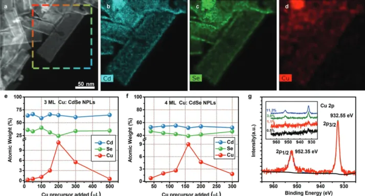
To investigate the Cu doping of the NPLs, HAADF STEM image of Cu-doped 3 ML CdSe NPLs (for the exemplary case of 1.1 atomic weight (at. wt.)% of Cu-doping) presented in Figure 1a, together with the EDS elemental map of Cd, Se, and Cu given in Figure 1b–d clearly shows the homogenous doping of Cu atoms within the core NPLs. Both Cd and Se maps are well matched with the HAADF-STEM image. At small doping levels, Cu maps also match the HAADF-STEM image. To differ-entiate the background, we recorded the EDS spectra for Cu on and off the NPL surface and shown in Figure S2 (Supporting Information). There is a clear difference in Cu K-alpha peak for maps on and off the particle, suggesting that these NPLs are doped with Cu. Additional EDS, TEM, and high-resolution TEM analysis for 3 and 4 ML Cu-doped and undoped NPLs are depicted in Figures S1–S8 (Supporting Information). The XRD patterns acquired from the undoped and doped NPLs show their characteristic peaks arising from the zinc-blende struc-ture (Figure S9, Supporting Information). Detailed selected area electron diffraction (SAED) analysis for the Cu (0%–9.0%) doped NPLs suggests consistent decrease in lattice d-spacing with constant increase in Cu doping levels in the host matrix of CdSe NPLs (Figure S10 and Table S1, Supporting Informa-tion). Similar results exist in the previous literature showing a constant decrease of (111) lattice planes d-spacing with increase of Cu doping amounts in CdSe QDs.[13]
To determine the exact doping amounts, ICP-MS measure-ments were carried out for the samples thoroughly cleaned with ethanol. Figure 1e,f shows the change of the Cd, Se, and Cu atomic percentages in the 3 and 4 ML doped NPLs as a
function of the added Cu precursor during the synthesis. From this set of analyses, we observed that there is a monotonic increase in the incorporated Cu dopant with the increase in Cu precursor up to a certain level. With the further increase in Cu precursor, the amount of Cu doping in the NPLs is found to decrease. Thus, the dopant concentration can be fine-controlled up to 11.3% for 3 ML and 9.0% for 4 ML NPLs by tuning the amount of Cu precursor solution used during synthesis.
Besides the EDS elemental maps and ICP measurements, XPS measurements independently show the presence of Cu in the NPLs, additionally providing further insight to understand its possible oxidation states. The high-resolution XPS spectra of 11.3% Cu-doped 3 ML CdSe NPLs shown in Figure 1g at 932.55 and 955.35 eV specific to Cu 2p orbitals suggesting the exist-ence of Cu+ ions as the dopant.[15,38,39] High-resolution XPS spectra at the Cu 2p peak are presented in the inset of Figure 1g as a function of the increasing Cu-dopant amount. Additional XPS analysis, survey-spectrum and high-resolution XPS for Cd and Se are given in Figure S11 (Supporting Information).
Figure 2a depicts the UV–visible absorption and steady-state PL spectroscopy results obtained from the samples of undoped and Cu-doped 3 and 4 ML CdSe NPLs. UV–visible absorption spectra of the undoped and doped samples show that both elec-tron heavy-hole (e-hh) and elecelec-tron light-hole (e-lh) transitions of the CdSe NPLs stay unchanged after doping, which pinpoints that the doping level studied here does not change the essential excitonic absorbance of the NPLs.[31] In addition, for all of the doped samples, there exists a very weak and broad absorption tail at lower energies beyond the first excitonic absorption peak (Figure S12, Supporting Information). This may arise due to metal-to-ligand (conduction band) charge transfer (MLCBCT)
absorption state, which has been previously observed for the Cu-doped CdSe CQDs.[40–42]
The PL emission spectrum of the undoped 3 ML CdSe NPLs in solution at room temperature (along with their normalized absorption spectrum) shown in Figure 2a exhibits a spectrally narrow band-edge (BE) emission peak at ≈465 nm having a full-width at half-maximum (FWHM) of ≈10 nm, which is a characteristic of the CdSe NPLs having 3 ML vertical thick-ness.[31] Along with the narrow BE emission, these NPLs also exhibit weak trap emission bands having a broad emission, which was reported earlier for these 3 ML NPLs.[30,35] On the contrary, for the doped 3 ML NPLs, a strong and broad emis-sion in the longer wavelength region (peaking at ≈650 nm) was observed in addition to the weak BE emission at ≈465 nm. This broad Stokes-shifted emission was previously assigned to Cu-related emission (MLCBCT) in CdSe CQDs.[13,41] UV–visible and PL emission spectra of undoped and Cu-doped 4 ML CdSe in Figure 2a show similar behavior with the doping of Cu ions, which has resulted in strong and efficient Stokes-shifted emis-sion (≈700 nm) for Cu-doped 4 ML NPLs. Thus, with the relaxa-tion of the confinement from 3 to 4 ML NPLs, we found con-sistent behavior in the shift of Cu-related emission spectrum (650–700 nm). The real-color photographs of both the undoped and Cu-doped 3 and 4 ML CdSe NPLs illuminated under UV lamp are given next to the corresponding emission spectra. Figure 2b shows energy band diagram for the undoped and Cu-doped NPLs. Therefore, as seen from emission spectrum in Figure 2a and its corresponding band diagram in Figure 2b, the recombination mechanism for this Cu+ related midgap emis-sion in these doped NPLs is very similar to 0D Cu-doped CdSe CQDs.[19,40,41,43]
Figure 1. a) HAADF-STEM images of 1.1% of Cu-doped 3 ML CdSe NPLs. b–d) EDS maps of cadmium, selenium and copper. e,f) ICP:MS analysis of
3 and 4 ML Cu-doped NPLs having different Cu precursors used during synthesis. g) High-resolution XPS spectra of Cu 2p region in 3 ML Cu (11.3%) doped CdSe NPLs (inset: high-resolution spectra for different Cu concentrations in CdSe NPLs).
Furthermore, as shown in Figure 2c, the Cu-related emis-sion contributions in the total emisemis-sion spectrum and absolute PL QE vary as a function of the increasing Cu precursors in the 3 and 4 ML doped NPLs. With increasing Cu precursor values up to certain levels (200 µL for 3 ML doped NPLs and 160 µL for 4 ML doped NPLs), the fraction of total integrated PL intensity associated with Cu+ emission (I
CT/ITOT) increases and the intensity of the excitonic PL decreases to nearly zero. Above these levels of dopant precursors, the integrated dopant related emission contributions decrease in consistency with the recovery of the BE emission. Additionally, as estimated by ICP:MS analysis, there is a monotonic increase in the doping percentage with respect to the added Cu precursors (e.g., up to 11.3% and 9.0% for 200 and 160 µL of the used precursors for 3 and 4 ML NPLs, respectively (Figure 1e,f)). Above these limits, further increasing amounts of the added Cu precursors during synthesis result in decreased doping percentages in the syn-thesized NPLs. Recently, for Cu-doped CdSe CQDs, a similar decrease in the Cu+ doping amounts at higher added amounts of the precursors has been observed, which further leads to the recovery of BE emission in their studies.[44] Detailed steady-state
PL emission and UV–visible absorption spectroscopy results for different Cu-doped 3 and 4 ML NPLs are presented in Figures S12 and S13 (Supporting Information).
To this end, we measured the absolute PL QEs of all doped and undoped NPLs using an integrating sphere based on de Mello method (Figure 2c).[45] Apart from the increase in dopant emission contributions (Cu+ PL fraction), the absolute PL QE also increases with the increase of Cu feed up to 100 and 120 µL for 3 and 4 ML doped NPLs, respectively. At these dopant feed values, the highest achieved PL QEs are 80% and 97% for 3 and 4 ML doped CdSe NPLs, respectively. With further increase in the Cu feed values, although the integrated Cu+ PL fraction increases slightly, the absolute PL QE decreases. These high PL QEs (≈80%–97%) for these Cu-doped 3 and 4 ML CdSe NPLs are found to be highly reproducible and stable at the ambient conditions for several months. Furthermore, these high PL QEs are nearly constant even at higher optical densities (from ≈0.01 to 2.00 at the e-hh peak measured in 1 mm path length) of the dispersions thanks to their large Stokes shift (Figure S14, Supporting Information). Recently, doped NCs (e.g., Cu-doped CdSe CQDs) possessing Stokes-shifted emission have been
Figure 2. a) UV–visible absorption and PL spectra of 3 and 4 ML Cu-doped and undoped CdSe NPLs. Color pictures of the 3 ML and 4 ML undoped
and Cu-doped CdSe NPLs illuminated by 365 nm UV lamp are shown next to the corresponding PL spectra. b) Energy band diagram for the undoped and Cu-doped NPLs. Herein, solid arrows show processes involving photons, and dashed arrows show nonradiative processes. c) ICT/ITOT and absolute
PL QE measured from the 3 and 4 ML Cu-doped NPLs plotted versus added Cu precursor values used in the reaction. d) Electronic absorption (solid, blue, and red), and PLE (dotted, blue and red, monitored at 650 and 700 nm for 3 and 4 ML NPLs, respectively) spectra of Cu-doped CdSe NPLs. e) TRF decays of the trap- and Cu-related emission at room temperature for undoped and Cu-doped 3 and 4 ML CdSe NPLs, respectively. f) UV–visible absorption and PL spectra of undoped 3 + 1 (i.e., CdSe/CdS), doped 3 + 1 ML (i.e., CdSe:Cu/CdS), undoped 4 + 1 (i.e., CdSe/CdS), and doped 4 + 1 (i.e., CdSe:Cu/CdS) core–shell NPLs.
shown to be the best in class luminophores for full spectrum LSCs, although they only reach the PL QE as high as 40%.[8] Thus, near-unity PL QE for our core only doped CdSe NPLs offers the potential to show significant improvement in the LSC applications.
To further understand the origin of this highly efficient and large Stokes-shifted emission in the doped NPLs, we performed PL excitation (PLE) spectroscopy (Figure 2d), collected while monitoring at the long-wavelength emission peak (650, 700 nm for 3 and 4 ML Cu-doped NPLs). These exhibit the midgap and both e-hh and e-lh transitions of the CdSe NPLs at the same relative intensity as in the electronic absorption spectrum (Figure 2d). Furthermore, excitation spectra of the Cu-doped 3 and 4 ML CdSe NPLs measured at spectral positions of the long-wavelength emission peak (i.e., at the peak, red-, and blue-tails), do not show any discernible spectral difference with respect to the electronic absorption spectrum (Figure S15, Supporting Information). This suggests that there is no inhomogeneous broadening in the doped NPLs owing to their magic-sized ver-tical thicknesses. Thus, unlike colloidal CQDs there is a near step-like optical absorption profile in these NPLs. Moreover, the PLE intensity for dopant related emission is much higher than BE-related emission for both 3 and 4 ML Cu-doped NPLs. Thus, it is clear from both the PL and PLE measurements that Cu doping has resulted in strong and efficient dopant-related Stokes-shifted emission in both 3 and 4 ML NPLs. Apart from the doping concentration, the type of NPL (thickness, lateral area), addition timing of the dopant precursor during synthesis, and different ligands used to prepare the dopant precursors are also important factors that are responsible for dominant and efficient Cu-related emission from NPLs (Figures S13 and S16, Supporting Information).
Furthermore, TRF spectroscopy using the time-correlated single-photon counting system was performed to understand this efficient dopant related emission in doped NPLs (Figure 2e). To investigate the exciton dynamics of this Stokes-shifted and highly efficient Cu+-related emission in the doped NPLs, we compared the PL decay curves in the doped and undoped NPLs at the long wavelength (trap emission for the undoped NPL and Cu emission in the doped NPL). In the pure 3 ML undoped NPLs, a very broad but weak defect emission is observed. The fluorescence decay curve of this defect emission is shown in Figure 2e (upper panel), where we also compared this decay to the decay of the dopant emission in the doped NPLs. There is a stark contrast between the decay curves, which implies that this large Stokes-shifted emission in the doped NPLs is not due to the surface trap states. This supports that this emission originates from the recombination of excited states between the conduction band of the CdSe NPL and the localized hole state of the Cu+ dopant.[40] Similar observations for the trap and Cu-related PL emission are also made for 4 ML doped and undoped CdSe NPLs (Figure 2e, lower panel). Cu-doped CdSe CQDs were previously shown to have an average lifetime between 300 and 500 ns.[19] The decay curves for both dopant and trap related emissions were fitted well with three expo-nentials for 3 ML and two expoexpo-nentials for 4 ML doped NPLs. The average lifetime for Cu+ and trap-related emissions in 3 and 4 ML doped and undoped NPLs were calculated as 278.3, 42.5 ns and 465.2, 211.2 ns, respectively (Tables S2 and S3,
Supporting Information). Briefly, absence and less fractional contribution of fast decay component in 4 and 3 ML Cu-doped NPLs, respectively, and positive correlation of Cu-related life-time component with absolute PL QEs explain the origin of high PL QE in these doped NPLs. Moreover, detailed analyses of different decay channels and their relative contributions for dopant related emission help to understand near-unity PL QEs for these newly synthesized NPLs (Figures S17 and S18, Tables S2 and S3, Supporting Information).
There have been several reports for the origin and photo-physics of Cu-related emission in CdSe NCs.[13,21,41] Although emergence of dopant related emission in these newly synthe-sized CdSe NPLs appears to be similar to the CQDs, further investigations were performed to understand its behavior. Moreover, unlike 4 ML undoped CdSe NPLs, 3 ML undoped NPLs possess a weak and broad trap-related emission, which can be confused with dopant related emission in these newly synthesized doped NPLs.
Even though we verified the presence of variable amount of Cu in these doped NPLs by different elemental techniques, the origin of this highly efficient and Stokes-shifted emission in these NPLs needs to be further investigated. To this end, we selected two different, 3 and 4 ML Cu-doped and undoped CdSe NPLs. Using these four NPLs separately as seeds we grew 1 ML shell of CdS via colloidal atomic layer deposition (c-ALD) technique.[46] Figure 2f shows the absorption and PL emission of the Cu-doped and undoped, 3 and 4 ML core/shell NPLs, respectively. In both the cases for 3 and 4 ML Cu-doped CdSe NPLs, the deposition of 1 ML of CdS shell redshifts the dopant emission further toward NIR region, which results from the relaxation of the confinement in the system. On the other hand, in the case of undoped NPLs with the deposition of 1 ML CdS shell, only excitonic emission is shifted to red regions and is in well agreement with previously reported undoped core/shell NPLs.[46] Due to the effective passivation of surface-related trap states with the CdS shell, trap-related emission in undoped 3 ML CdSe NPLs is completely suppressed. Therefore, appear-ance of this dopant-related redshifted-emission in the case of Cu-doped 3 ML core–shell NPLs supports that this broad Stokes-shifted emission in doped NPLs has not been originated from the surface-related trap sites. Furthermore, all excitonic features are well preserved in the doped samples as compared to undoped NPLs after growing the shell. However, with the deposition of 1 ML of shell there is a significant decrease in the measured absolute PL QEs (e.g., 70% to 12% and 90% to 18% for 3 and 4 ML samples, respectively). Furthermore, with the deposition of CdS shell, the Cu-related emission contributions are observed to decrease with the consistent recovery of BE emissions for both 3 and 4 ML Cu-doped NPLs. Recently, near complete elimination of Cu dopant ions and its related emis-sion has been observed for Cu-doped CdSe CQDs after over-coating these doped CQDs with CdS shell.[44] The authors have accounted this extraction of Cu ions to the ability of different amines to access NC surface, which are used in the shell growth procedures. In our case for doped NPLs, rigorous cleaning steps and use of oleylamine during the shell growth with c-ALD approach suggest similar behavior for the extraction of Cu ions during shell growth. Overall, these initial results are supportive to show that these highly efficient and Stokes-shifted emissions
in 3 and 4 ML doped NPLs are originated from the MLCBCT PL emission like the previously studied 0D Cu-doped CdSe CQDs.
Successful Cu+ doping leading to highly efficient dopant-related emission in our doped NPLs, creates a material platform as possible luminophores for LSC applications. The Cu-doped CQDs have been recently shown to be the best phosphors for short- and long-scaled LSCs.[8] Although PL QE of these Cu+-doped CQDs has been shown to be moderately low (in the range of 40%)[8,19] in comparison to other NC heterostruc-tures,[2,8] their tunable solar absorption and lower reabsorption losses increased their performance as LSC luminophores. In our work, Cu+ doping in 2D CdSe NCs has shown near-unity PL QE with similar Stokes-shifted emission. To characterize the performance of our doped 3 and 4 ML NPLs as LSC lumino-phores, we compared them with benchmarked Cu-doped CdSe CQDs (having PL QE of 44%) in terms of reabsorption losses in the solution. Details of the synthesis, elemental characteriza-tion, steady-state spectroscopy and lifetime spectroscopy results for the doped CdSe CQDs are presented Figures S19 and S20, Table S4 (Supporting Information).
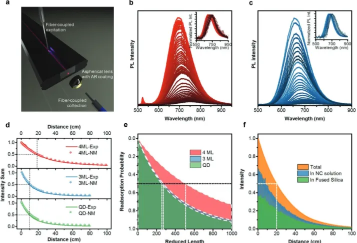
We measured the reabsorption losses in the NPLs using a recently reported 1D liquid waveguide with an excitation source placed on a movable stage[8] (Figure 3a). The experimental setup
that is adapted with some modifications is given in Figure S21 (Supporting Information). The movable excitation source simu-lates the optical path distance to the stationary emission detec-tion spectrometer coupled via a multimode optical fiber and a lens system. Reabsorption losses are quantified by measuring the PL spectra as a function of the optical path distance, L, up to 1.2 m. To make a fair comparison in terms of the reabsorp-tion losses, we prepared 3 and 4 ML Cu+ doped NPL solutions having unity optical densities (OD = 1) over t = 1 mm (which is the thickness of the quartz cuvette) at their e-hh absorption peaks. The solutions were carefully injected into the hollow fused silica waveguide without creating any air bubble in the optical path (since air bubbles can create unwanted artificial scattering centers). The PL emission spectra were collected by sliding the excitation source to systematically varied values of
L, where L is the optical path distance between the excitation
source and the collection end of the waveguide. Figure 3b,c shows the PL spectra of 3 and 4 ML doped NPLs with changing
L. The PL intensity decreases with a redshift in the spectrum
with the increasing L for all luminophores. This decrease in the PL emission intensity and the accompanying redshift in the PL emission spectra of these highly concentrated solutions of the doped NPLs are accounted for the reabsorption losses on the
Figure 3. a) Illustration for 1D LSC measurement. b,c) 4 ML, 3 ML NPL PL intensities at different optical distances. Insets show the normalized PL
emission of the same data to visualize redshift in the PL emission clearly. d) Spectrally integrated PL intensities for different luminophores as a func-tion of excitafunc-tion distance by both experimental and numerical modeling. e) Reabsorpfunc-tion probability, plotted versus reduced length. f) Monte Carlo ray tracing simulation for the intensity decay using 4 ML NPL absorbance at the dopant emission and PL QE values. The dashed lines in (d–f) indicate half-lengths, which for a given sample represent the value of length corresponding to 50% probability of reabsorption.
higher energy side of the PL emission spectrum. The normal-ized PL emission spectra for the doped 3 and 4 ML NPLs are shown in the insets of Figure 3b,c. The PL peak emission wave-length and half-maximum wavewave-length values of the measured PL spectra are given in Figure S22 (Supporting Information). While 3 and 4 ML NPLs exhibit a redshift, CQDs show a nar-rowing in the PL emission spectra from the both sides causing the PL intensity to decrease significantly.
To understand the redshift and decrease in the PL spectrum, a numerical modeling using Beer–Lambert law is performed. For all samples, the change in the PL spectra with optical path distance obeys Beer–Lambert law perfectly, making the theoret-ical analysis possible on the LSC luminophores. In Figure S23 (Supporting Information), we compared the experimental and modeled PL spectra for all optical distances, which are in good agreement. Hence, using only the absorption and PL emission spectra of the emitters, it is possible to completely simulate the PL emission spectrum at any optical distance devising a useful method to characterize the performance of the lumino-phores to be used as LSC materials. Figure 3d shows the inte-grated PL emission intensities as a function of L for all of the luminophores shown in Figure S23 (Supporting Information) (normalized at the collection end of the 1D waveguide, i.e.,
L = 0). Unlike previously reported studies,[2,8] these integrated PL emission data were not corrected for any waveguide or scattering related losses. Although the scattering losses in the solutions are expected to be negligible due to the size of the luminophores, they have been already included in the absorb-ance spectra. Excellent agreement of the numerical model per-formed using Beer–Lambert law with experimental measure-ments also suggests that the only significant loss mechanism is the reabsorption loss in the solution.
To reduce the effect of the reabsorption losses in the wave-guide, we prepared dilute solutions of the 4 ML NPLs. 50 and 100 times diluted solutions of 4 ML doped NPLs do not show any noticeable PL emission intensity decrease that can be attrib-uted to scattering or waveguide related losses in Figure S24 (Supporting Information). Agreement between experimen-tally measured and numerically modeled integrated PL emis-sion intensities in Figure 3d indicates that at such high optical densities (OD = 1) the dominating loss mechanism in the 1D waveguide stems from the reabsorption. In the numerical mod-eling, we used an effective confinement factor, Γ (<1), which quantifies how much of the emitted light is confined in the luminophore solution (i.e., the core region) of our waveguide. The best matching Γ factor is 0.3 for all luminophores in our setup. The LSC half length (L1/2) values[47] calculated from Figure 3d, for 3 ML and CQDs are nearly similar (≈10.0 cm), whereas 4 ML doped NPLs are shown to possess significantly longer L1/2 (≈18.5 cm). In Figure 3e, we calculated the reabsorp-tion probability to compare the LSC performances of the lumi-nophores by considering their absorbance and PL emission profiles.[8] Details of the calculations can be found in Section SII (Supporting Information). Reabsorption probability also provides a similar performance metric for the luminophores; 3 ML NPLs perform slightly better than the benchmarked CQDs and the performance of 4 ML NPLs substantially exceeds those of the other two. Ray-tracing Monte Carlo simulation using the absorbance and PL QE values of 4 ML NPLs predicts the
half-length as ≈19.5 cm, which is close to the experimentally measured 18.5 cm (Figure 3f).
In the light of experimental analyses and numerical model of the reabsorption losses, it is possible to project the flux gain (FG) performance of these doped NPLs. Previously, Gamelin and co-workers have reported the projected FG for 1D LSCs using the experimentally derived reabsorption data for different LSC emitters, e.g., doped NCs and different heterostructures.[8] In their work, despite low PL QEs, Cu-doped CdSe CQDs have shown the highest FGs for short- and long-range LSCs. In our case, 3 ML NPLs have a small spectral overlap with the solar spectrum; however, thanks to their higher PL QEs, 3 ML NPL FG performance is close to CQDs (Figure 4a). In addition to its low reabsorption loss performance, the absorption profile of 4 ML doped NPLs is redshifted with respect to 3 ML doped NPLs. This redshift in the absorption increases the overlap of the absorbance spectrum of the 4 ML NPLs with the solar emission. Having near-unity PL QE and increased spectral overlap with the solar spectrum compared to 3 ML NPLs, 4 ML NPLs sig-nificantly outperform CQDs as expected from the integrated PL intensity measurements in Figure 3d. Although the absorption profile of Cu-doped NPLs have limited spectral overlap with the solar emission in comparison to Cu-doped CQDs, their near-unity PL QEs and step-like optical absorption have resulted in higher FGs for these newly synthesized LSC emitters.
After characterization of our luminophores in solution form, LSC prototypes have been prepared by embedding our Cu-doped luminophores in polymer matrix as a proof-of-concept demonstration. Poly(lauryl methacrylate) (PLMA) has been used as the polymer host material since its long side chains prevent agglomeration of colloidal NCs and low optical absorption in the visible spectrum allows for the fabrication of high-quality CQD- and CQW-polymer nanocomposites.[6,36,48] Cu-doped CQD-PLMA (and CQW-PLMA) nanocomposite between two borofloat glasses separated by transparent acrylic tape was photopolymerized with two 365 nm UV sources from the both sides for uniform illumination. In the process of nanocomposite photopolymerization, we used an earlier reported fabrication procedure with little modifications (Sec-tion SI, Supporting Informa(Sec-tion).[6,48] After the polymerization step, these 2D LSC plates were used as such for the measure-ments. In Figure 4b, high quality fabrication of the samples with high transmissivity is presented. Demonstrations of different LSCs under ambient light and UV light conditions are also given in Figures S28 and S29 (Supporting Informa-tion). Illustration of the Cu-doped 3 ML incorporated 2D LSC under UV illumination shows that the emitted light is con-centrated to the edges (Figure 4c). In Figure 4d, absorbance and PL emission spectra for 3 and 4 ML NPLs in solution and in PLMA are presented. For both the 3 and 4 ML NPLs, we observed that our luminophores remain unaffected in terms of their steady-state spectral behavior when incorporated in PLMA. Furthermore, the PL emission decay dynamics were analyzed in toluene, lauryl methacrylate (LMA) monomer solution and PLMA polymer film for the 3 and 4 ML NPLs without a noticeable change with respect to the matrix condi-tions, which indicates successful incorporation of these doped NPLs in the polymer matrix (Figure 4e and Table S5, Sup-porting Information).
Using small slabs of dimensions (1 × 1 cm2), we measured optical efficiencies of all the studied doped luminophores by using a calibrated integrating sphere.[11] The highest meas-ured optical efficiencies are 52.5%, 46.5%, and 13.5% for the LSCs fabricated using Cu-doped 3 ML NPLs, 4 ML NPLs, and
QDs, respectively. To make a fair performance evaluation of the luminophores, we used the absorbed photon flux (A), which is calculated by the integration of the overlap product of the lumi-nophore absorption and the solar flux (Section SII, Supporting Information). Since three of the luminophores are absorbing
Figure 4. a) 1D FGs for different LSC luminophores. b) 2D LSCs consisting of Cu-doped 3 ML, 4 ML NPLs, and QDs incorporated in PLMA showing
their high uniformity and high transmissivity under daylight. c) The real-color photograph of fabricated 3 ML NPL, 10 × 10 cm2 LSC incorporated in
PLMA matrix shown under UV illumination. d) UV–vis absorption and PL spectra of Cu-doped 3 and 4 ML NPLs in toluene solution and in PLMA matrix. e) PL decay curves of 3 and 4 ML NPLs in toluene, LMA monomer solution and in PLMA solid films. f) Measured optical efficiencies at dif-ferent A values of the 3 and 4 ML samples and one concentration for the QD sample. Inset shows measured quantum efficiency of final devices using integrating sphere. g) Calculated flux gain values for G = 25 case with the measured PL QEs in the PLMA polymer matrix and with in-solution PL QEs for determining upper performance limit. h) Similar calculated flux gain values for LSCs having G = 250.
different portions of the solar spectrum, this definition can be a useful metric for assessing their performance. Moreover, con-sidering the constant external QE response of the commercial silicon solar cells, effect of the PL emission wavelength of the luminophores on the efficiency of the solar cell should be negli-gible.[8] In Figure 4f, measured optical efficiencies (η
opt) for dif-ferent loadings of NPLs in PLMA matrix with one loading of QD is shown when an Si solar cell is attached to one edge of the LSC. Measured short-circuit current, open-circuit voltage, and filling factor values are given in Figure S30 (Supporting Infor-mation). In all the measurements, no back diffuser or reflector was located at the back of the waveguide in order to reproduce the situation of an actual PV window illuminated by the sun light. For a 10 × 10 cm2 lateral area of the LSC, emitted light is confined to edges having an area of 10 × 0.1 cm2. Thanks to their preserved PL QEs (≈70.0%) in PLMA matrix, the 3 ML NPLs showed ηopt = 1.65% at 1.59 × 10²⁰ photons m−2 s−1, while the QDs showed ηopt= 1.52% at 2.32 × 10²⁰ photons m−2 s−1. Despite the lower spectral overlap of 3 ML NPLs with the solar irradiation, higher loadings of the 3 ML samples absorbing less solar flux can generate higher outputs of electrical power. 4 ML NPLs showed relatively poor performance as compared to 3 ML NPLs due to their significantly lowered PL QE value (≈40.0%) in PLMA matrix compared to their in-solution PL QEs (≈92.0%). In Figure 4g,h, calculated flux gains for the G = 25 and G = 250 cases (where G is the geometrical gain coefficient computed as the ratio of the lateral acceptance area of the LSC to the total area that solar cells can be attached around the periphery) are showing promising results for our highest meas-ured in-solution PL QEs of 4 ML NPLs, which can reach above
FG = 0.2 value for G = 25 and above FG = 7.5 for G = 250. In the case of G = 250, effect of the 4 ML NPL step-like absorption profile provides a very steep FG enhancement for low absorbed photon flux values and after a certain A value, FG decreases very rapidly.
These results clearly show the great potential of these doped NPLs to be used in large-scale LSC applications. However, in order to obtain performance better than that of 3 ML doped NPLs, further optimization of process parameters of 4 ML Cu-doped NPLs is required to retain high PL QE in PLMA matrix. Recently, coating of colloidal CQDs on glass slides using doctor blade technique has been shown to achieve high PL QE in 2D LSCs.[5] Thus, these newly shown Cu-doped NPLs possessing superior optical properties have the potential to be engi-neered with further optimization of fabrication procedures for retaining high PL QEs in the film form. Moreover, by extending this doping strategy in these 2D CQWs having slightly higher thickness (e.g., Cu-doped 5–11 ML CdSe, CdSe/CdS core–shell and core–crown architectures), the absorption spectrum can be further tuned to absorb more solar light and emit in the NIR. Therefore, the present work provides a solid platform for applying doping concepts in 2D colloidal quantum wells, which can be extended into different dopant/core and new 2D archi-tectures for future solar light harvesting applications.
In conclusion, we have shown the first core doping of 2D CdSe colloidal quantum wells with Cu enabling exceptional optical properties including step-like optical absorption, tun-able emission in the visible-to-NIR spectral region, large Stokes shift, near-unity PL QE, and high absorption cross-section.
Detailed HAADF-EDS, ICP, XPS, steady-state, and time-resolved fluorescence spectroscopy studies confirm the copper doping in CdSe CQWs. The combination of stable and domi-nant dopant related emission having minimum self-absorption accompanied with significantly unchanged PL QE at higher optical densities augment the novelty and advantage of deep substitutional doping of Cu+ in CdSe CQWs. Under similar experimental and numerical conditions, these doped CQWs are shown to be excellent LSC emitters; outperforming typical doped CQDs. Based on these unique properties, a prototype of LSC has been demonstrated. We believe that doping in CQWs can be extended to different types and thicknesses of materials, and different transition metal elements, which could expand potential applications in various optoelectronic and color con-version devices.
Experimental Section
Chemicals: Cadmium nitrate tetrahydrate, sodium myristate, technical
grade 1-octadecene (ODE), selenium, cadmium acetate dihydrate, copper (II) acetate, trioctylphosphine (TOP), oleylamine, ammonium sulfide, N-methylformamide, and technical grade oleic acid (OA) were purchased from Sigma-Aldrich. Methanol, ethanol, acetone, and hexane were purchased from Merck Millipore.
Synthesis of Cu-Doped 3 ML Thick CdSe Nanoplatelets: Cd(Ac)2·2H2O
(0.5 mmol), oleic acid (0.3 mmol), and ODE (15 mL) were mixed in a 50 mL three-neck flask. After stirring and Ar bubbling for 10 min, different amounts of Cu precursors (20–500 µL) were added at room temperature. Subsequently, the flask was heated to 230 °C under Ar protection. After the flask was kept at 230 °C for 5 min, Se-ODE solution (2.5 mL) was injected and immediately light yellow color appeared. Although the temperature of solution decreases by the addition of Se precursor, slow heating with external heat gun for 1 min helps to retain the temperature level at 230 °C, which was maintained for additional 4 min. After that, the temperature of the solution was decreased to room temperature using a water bath. The solution was centrifuged at 2500 rpm for 10 min and the supernatant was removed into another centrifuge tube. After adding ethanol into the supernatant solution until the occurrence of turbidity, the solution was centrifuged again at 8000 rpm for 5 min, and then the precipitates were dissolved and stored in toluene. An undoped control reaction was performed by injecting 100 µL of bare TOP-ODE at the start having same concentrations used for preparing Cu-TOP precursor.[37]
Synthesis of Cu-Doped 4 ML Thick CdSe Nanoplatelets: For a typical
synthesis, 340 mg of cadmium myristate, 24 mg of Se, and 30 mL of ODE were loaded into a 100 mL three-neck flask. The solution was degassed and stirred at 95 °C under vacuum for 1 h in order to evaporate volatile solvents and dissolve the cadmium myristate completely. Then, the heater was set to 240 °C and the vacuum was broken at 100 °C and the flask was filled with argon gas. As the temperature reached 190 °C, variable amounts of Cu precursor (40–300 µL) already prepared and stored in nitrogen filled glove box was added dropwise until the temperature reached 195 °C where the color of the solution became yellowish and then 120 mg of cadmium acetate dihydrate was introduced swiftly into the reaction. After the growth of CdSe NPLs at 240 °C for around 10 min, 1 mL of OA was injected and the temperature of the solution was decreased to room temperature using a water bath. The solution was centrifuged for 5 min at 6000 rpm and the supernatant was removed into another centrifuge tube. After adding ethanol into the supernatant solution until it became turbid, the solution was centrifuged again at 10 000 rpm for 5 min, and then the precipitates were dissolved and stored in toluene. The small subpopulations of undoped small sized 5 ML CdSe NPLs remained in supernatant in this centrifugation step, which was discarded. An undoped control reaction
was performed by injecting bare 100 µL of TOP-ODE solutions with the same concentrations used for preparing Cu-TOP precursors.
Supporting Information
Supporting Information is available from the Wiley Online Library or from the author.
Acknowledgements
M.S. and K.G. contributed equally to this work. The authors gratefully acknowledge the financial support from the Singapore National Research Foundation under the programs of NRF-NRFI2016-08 and NRF-CRP-6-2010-02 and the Science and Engineering Research Council, Agency for Science, Technology and Research (A*STAR) of Singapore; EU-FP7 Nanophotonics4Energy NoE; and TUBITAK EEEAG 114E449 and 114F326. H.V.D. acknowledges the support from ESF-EURYI and TUBA-GEBIP. M.S. would like to thank TUBITAK BIDEB 2221 program. K.G., Y.K., and T.E. acknowledge support from TUBITAK BIDEB 2211 program.
Conflict of Interest
The authors declare no conflict of interest.
Keywords
2D semiconductor nanoplatelets, copper doping, luminescent solar concentrators, nucleation doping, quantum efficiency
Received: February 9, 2017 Revised: April 18, 2017 Published online: June 12, 2017
[1] A. Goetzberger, W. Greubel, Appl. Phys. 1977, 14, 123.
[2] F. Meinardi, A. Colombo, K. A. Velizhanin, R. Simonutti, M. Lorenzon, L. Beverina, R. Viswanatha, V. I. Klimov, S. Brovelli,
Nat. Photonics 2014, 8, 392.
[3] M. G. Debije, P. P. C. Verbunt, Adv. Energy Mater. 2012, 2, 12. [4] M. J. Currie, J. K. Mapel, T. D. Heidel, S. Goffri, M. A. Baldo, Science
2008, 321, 226.
[5] H. Li, K. Wu, J. Lim, H.-J. Song, V. I. Klimov, Nat. Energy 2016, 1, 16157.
[6] F. Meinardi, H. McDaniel, F. Carulli, A. Colombo, K. a. Velizhanin, N. S. Makarov, R. Simonutti, V. I. Klimov, S. Brovelli, Nat.
Nano-technol. 2015, 10, 878.
[7] K. E. Knowles, T. B. Kilburn, D. G. Alzate, S. McDowall, D. R. Gamelin, Chem. Commun. 2015, 51, 9129.
[8] L. R. Bradshaw, K. E. Knowles, S. McDowall, D. R. Gamelin, Nano
Lett. 2015, 15, 1315.
[9] J. Bomm, A. Büchtemann, A. J. Chatten, R. Bose, D. J. Farrell, N. L. A. Chan, Y. Xiao, L. H. Slooff, T. Meyer, A. Meyer, W. G. J. H. M. Van Sark, R. Koole, Sol. Energy Mater. Sol. Cells 2011,
95, 2087.
[10] C. S. Erickson, L. R. Bradshaw, S. McDowall, J. D. Gilbertson, D. R. Gamelin, D. L. Patrick, ACS Nano 2014, 8, 3461.
[11] I. Coropceanu, M. G. Bawendi, Nano Lett. 2014, 14, 4097.
[12] N. D. Bronstein, Y. Yao, L. Xu, E. O’Brien, A. S. Powers, V. E. Ferry, A. P. Alivisatos, R. G. Nuzzo, ACS Photonics 2015, 2, 1576.
[13] R. W. Meulenberg, T. van Buuren, K. M. Hanif, T. M. Willey, G. F. Strouse, L. J. Terminello, Nano Lett. 2004, 4, 2277.
[14] A. H. Khan, A. Dalui, S. Mukherjee, C. U. Segre, D. D. Sarma, S. Acharya, Angew. Chem., Int. Ed. 2015, 54, 2643.
[15] A. Tang, L. Yi, W. Han, F. Teng, Y. Wang, Y. Hou, M. Gao, Appl. Phys.
Lett. 2010, 97, 033112.
[16] S. Jana, B. B. Srivastava, N. Pradhan, J. Phys. Chem. Lett. 2011, 2, 1747.
[17] W. Zhang, Q. Lou, W. Ji, J. Zhao, X. Zhong, Chem. Mater. 2014, 26, 1204.
[18] G. K. Grandhi, R. Tomar, R. Viswanatha, ACS Nano 2012, 6, 9751. [19] K. E. Knowles, K. H. Hartstein, T. B. Kilburn, A. Marchioro,
H. D. Nelson, P. J. Whitham, D. R. Gamelin, Chem. Rev. 2016, 116, 10820.
[20] J. Liu, Q. Zhao, J.-L. Liu, Y.-S. Wu, Y. Cheng, M.-W. Ji, H.-M. Qian, W.-C. Hao, L.-J. Zhang, X.-J. Wei, S.-G. Wang, J.-T. Zhang, Y. Du, S.-X. Dou, H.-S. Zhu, Adv. Mater. 2015, 27, 2753.
[21] A. Pandey, S. Brovelli, R. Viswanatha, L. Li, J. M. Pietryga, V. I. Klimov, S. A. Crooker, Nat. Nanotechnol. 2012, 7, 792.
[22] J. W. Stouwdam, R. A. J. Janssen, Adv. Mater. 2009, 21, 2916. [23] B. B. Srivastava, S. Jana, N. Pradhan, J. Am. Chem. Soc. 2011, 133,
1007.
[24] R. Xie, X. Peng, J. Am. Chem. Soc. 2009, 131, 10645.
[25] A. Sahu, M. S. Kang, A. Kompch, C. Notthoff, A. W. Wills, D. Deng, M. Winterer, C. D. Frisbie, D. J. Norris, Nano Lett. 2012, 12, 2587. [26] S. C. Erwin, L. Zu, M. I. Haftel, A. L. Efros, T. a. Kennedy,
D. J. Norris, Nature 2005, 436, 91.
[27] D. Mocatta, G. Cohen, J. Schattner, O. Millo, E. Rabani, U. Banin,
Science 2011, 332, 77.
[28] P. N. Tananaev, S. G. Dorofeev, R. B. Vasil’ev, T. A. Kuznetsova,
Inorg. Mater. 2009, 45, 347.
[29] A. M. Jawaid, S. Chattopadhyay, D. J. Wink, L. E. Page, P. T. Snee,
ACS Nano 2013, 7, 3190.
[30] S. Ithurria, B. Dubertret, J. Am. Chem. Soc. 2008, 130, 16504. [31] S. Ithurria, M. D. Tessier, B. Mahler, R. P. S. M. Lobo, B. Dubertret,
A. L. Efros, Nat. Mater. 2011, 10, 936.
[32] M. Olutas, B. Guzelturk, Y. Kelestemur, A. Yeltik, S. Delikanli, H. V. Demir, ACS Nano 2015, 9, 5041.
[33] A. Yeltik, S. Delikanli, M. Olutas, Y. Kelestemur, B. Guzelturk, H. V. Demir, J. Phys. Chem. C 2015, 119, 26768.
[34] B. Guzelturk, Y. Kelestemur, M. Olutas, S. Delikanli, H. V. Demir,
ACS Nano 2014, 8, 6599.
[35] C. She, I. Fedin, D. S. Dolzhnikov, P. D. Dahlberg, G. S. Engel, R. D. Schaller, D. V Talapin, ACS Nano 2015, 9, 9475.
[36] J. M. Pietryga, Y. Park, J. Lim, A. F. Fidler, W. K. Bae, S. Brovelli, V. I. Klimov, Chem. Rev. 2016, 116, 10513.
[37] D. Chen, Y. Gao, Y. Chen, Y. Ren, X. Peng, Nano Lett. 2015, 15, 4477. [38] A. Radi, D. Pradhan, Y. Sohn, K. T. Leung, ACS Nano 2010, 4, 1553. [39] Y. Wang, M. Zhukovskyi, P. Tongying, Y. Tian, M. Kuno, J. Phys.
Chem. Lett. 2014, 5, 3608.
[40] P. J. Whitham, K. E. Knowles, P. J. Reid, D. R. Gamelin, Nano Lett.
2015, 15, 4045.
[41] K. E. Knowles, H. D. Nelson, T. B. Kilburn, D. R. Gamelin, J. Am.
Chem. Soc. 2015, 137, 13138.
[42] A. Suzuki, S. Shionoya, J. Phys. Soc. Jpn. 1971, 31, 1455.
[43] J. T. Wright, K. Forsythe, J. Hutchins, R. W. Meulenberg, Nanoscale
2016, 8, 9417.
[44] L. Yang, K. E. Knowles, A. Gopalan, K. E. Hughes, M. C. James, D. R. Gamelin, Chem. Mater. 2016, 28, 7375.
[45] J. C. de Mello, H. F. Wittmannn, R. H. Friend, Adv. Mater. 1997, 9, 230. [46] S. Ithurria, D. V. Talapin, J. Am. Chem. Soc. 2012, 134, 18585. [47] A. A. Earp, G. B. Smith, P. D. Swift, J. Franklin, Sol. Energy 2004, 76,
655.
[48] H. Zhao, D. Benetti, L. Jin, Y. Zhou, F. Rosei, A. Vomiero, Small