High-speed >90% quantum-efficiency
photodiodes with a resonance wavelength
adjustable in the 795–835 nm range
Ekmel Özbay, Ïbrahim Kimukin, Necmi Biyikli, Orhan Aytür, Mutlu Gökkavas, Gökhan Ulu, M. Selim Ünlü,
Richard P. Mirin, Kris A. Bertness, and David H. Christensen
Citation: Appl. Phys. Lett. 74, 1072 (1999); doi: 10.1063/1.123485 View online: http://dx.doi.org/10.1063/1.123485
View Table of Contents: http://aip.scitation.org/toc/apl/74/8
Published by the American Institute of Physics
Articles you may be interested in
Resonant cavity enhanced photonic devices
Journal of Applied Physics 78, 607 (1998); 10.1063/1.360322
Extraction of Schottky diode parameters from forward current-voltage characteristics
High-speed
>
90% quantum-efficiency
p
–
i
–
n
photodiodes with a resonance
wavelength adjustable in the 795–835 nm range
Ekmel O¨ zbaya)and I¨brahim Kimukin
Department of Physics, Bilkent University, Bilkent, Ankara 06533, Turkey
Necmi Biyikli and Orhan Aytu¨r
Department of Electrical and Electronics Engineering, Bilkent University, Bilkent, Ankara 06533, Turkey
Mutlu Go¨kkavas, Go¨khan Ulu, and M. Selim U¨ nlu¨
Department of Electrical and Computer Engineering, Boston University, Boston, Massachusetts 02215
Richard P. Mirin, Kris A. Bertness, and David H. Christensen
Optoelectronics Division, National Institute of Standards and Technology, Boulder, Colorado 80303 ~Received 20 August 1998; accepted for publication 21 December 1998!
We report GaAs/AlGaAs-based high-speed, high-efficiency, resonant cavity enhanced p – i – n photodiodes. The devices were fabricated by using a microwave-compatible fabrication process. By using a postprocess recess etch, we tuned the resonance wavelength from 835 to 795 nm while keeping the peak efficiencies above 90%. The maximum quantum efficiency was 92% at a resonance wavelength of 823 nm. The photodiode had an experimental setup-limited temporal response of 12 ps. When the system response is deconvolved, the 3 dB bandwidth corresponds to 50 GHz, which is in good agreement with our theoretical calculations. © 1999 American Institute of
Physics. @S0003-6951~99!03708-0#
High-speed, high-efficiency photodetectors are vital components of optical communication and measurement systems.1 Both Schottky photodiodes,2–4 and p – i – n
photodiodes5,6 offer high-speed performance to fulfill the needs of such systems. However, the efficiency of these de-tectors has been typically limited to less than 10%, mostly due to the thin absorption region needed for short transit times. One can increase the absorption region thickness to achieve higher efficiencies, but this also means longer transit times that will degrade the high-speed performance of the devices. Resonant cavity-enhanced~RCE! photodetectors of-fer the possibility of overcoming this limitation in the bandwidth-efficiency product of conventional photo-detectors.7–9 The RCE detectors are based on the enhance-ment of the optical field within a Fabry–Perot resonant cav-ity. The increased field allows the use of thin absorbing lay-ers, which minimizes the transit time of the photogenerated carriers without hampering the quantum efficiency. High-speed RCE photodetector research has mainly concentrated on using p – i – n photodiodes10 and avalanche photodiodes, where 75% quantum efficiency along with a .20 GHz bandwidth,11and 3 dB bandwidths as high as 33 GHz12have been reported. Recently, we have fabricated RCE Schottky photodiodes with 50% quantum efficiency and a 50 GHz frequency performance.13,14In this letter, we report our work on design, fabrication, and testing of widely tunable, high-speed RCE p – i – n photodiodes for operation around 820 nm with significantly improved quantum efficiency.
The details of the epitaxial structure we have used in this work are given in the Table I. The bottom Bragg mirror is made of quarter-wave stacks (Al0.20Ga0.80As/AlAs) designed
for high reflectance at 820 nm center wavelength. The
struc-ture was grown by solid-source molecular beam epitaxy on a 50 mm diam semi-insulating GaAs substrate. Carrier trap-ping was avoided by using linear composition grading at interfaces of the absorbing layer. The active layer thickness d was chosen such that the maximum quantum efficiency is obtained by
R15R2e22ad, ~1!
where a is the absorption coefficient, R1 is the top air– semiconductor mirror reflectance, and R2 is the bottom Bragg mirror reflectance.7 The measured reflectance of the as-grown wafer along with transfer-matrix-method-based theoretical simulation of the same structure is shown in Fig. 1. The resonance occurs at 826 nm with a measured reflec-tance minimum of 5%, while our theoretical simulations pre-dict nearly zero reflectance at the same wavelength. The measured resonance wavelength changes from 826 nm at the center of the wafer, to 816 nm at the edge of the wafer. This epilayer thickness variation across the wafer and small
de-a!Electronic-mail: [email protected]
TABLE I. Epitaxial structure of the resonant cavity-enhanced p – i – n pho-todiode.
Material Doping~cm23! Thickness~nm!
GaAs p1231018 20
Al0.2Ga0.8As p1231018 200 Al0.2Ga0.8As→GaAs Undoped 38
GaAs Undoped 470
GaAs→Al0.2Ga0.8As Undoped 38 Al0.2Ga0.8As n1231018 390
Al0.2Ga0.8As Undoped 180
Bragg mirror~24 pairs! Semi-insulating GaAs
APPLIED PHYSICS LETTERS VOLUME 74, NUMBER 8 22 FEBRUARY 1999
1072
viations between growth and design explain the difference between the theoretical and experimental reflectance charac-teristics.
The samples were fabricated by a microwave-compatible process. First, Ohmic contacts to the n1layers were formed by a recess etch that was followed by a self-aligned Au– Ge–Ni lift-off. The p1 Ohmic contact was achieved by a Au/Ti lift-off. The samples were then rapid thermal annealed at 450 °C for 25 s. Using an isolation mask, we etched away all of the epilayers except the active areas. Then, we evapo-rated Ti/Au interconnect metal which formed coplanar wave-guide~CPW! transmission lines on top of the semi-insulating substrate. The next step was the deposition and patterning of a 210 nm thick Si3N4layer. Besides passivation and
protec-tion of the surface, the Si3N4was also used as the dielectric
of the metal–insulator–metal bias capacitors. Finally, a 1.0 mm thick Au layer was used as an airbridge to connect the center of the CPW to the p1 Ohmic contact. The resulting
p – i – n photodiodes had breakdown voltages greater than 14
V. The dark current of a 30mm diam circular device at21 V bias was 20 pA.
Photoresponse measurements were carried out in the 750–850 nm wavelength range by using a tungsten–halogen projection lamp as the light source and a single-pass mono-chromator. The output of the monochromator was coupled to a multimode fiber. The monochromatic light was delivered to the devices by a lightwave fiber probe, and the electrical characterization was carried out on a probe station. The spec-tral response was measured using a calibrated optical pow-ermeter. For photospectral measurement, large-area photo-diodes (250mm3250mm) were chosen to ensure all of the optical power is incident on the active area. The top p1 layers were recess etched in small steps, and the tuning of the resonance wavelength within the Bragg mirror’s upper and lower edges was observed. Figure 2~a! shows the spectral quantum efficiency measurements of a device obtained by consecutive recess etches. Plot 1 corresponds to the as-grown wafer, while plots 2, 3, 4, and 5 correspond to cumulative recess etches of 25, 50, 75, and 100 nm, respectively. The peak experimental quantum efficiency~88%! of the as-grown sample at 816 nm increases to .90% values after the top absorbing GaAs cap layer is removed. The peak quantum efficiency remains almost constant with tuning until the reso-nance wavelength reaches to the lower edge of the Bragg mirror~780 nm!. At this point, the second resonance appears
around the upper edge of the Bragg mirror. The maximum measured quantum efficiency of 92% is obtained when the second resonance is tuned to 823 nm. As seen in Fig. 2~a!, the resonance wavelength can be tuned for a total of 40 nm
~835–795 nm! while keeping peak efficiencies above 90%.
The peak efficiency is still above 85% for resonant wave-lengths between 780 and 840 nm, corresponding to a tuning range of 60 nm. The full width at half maximum~FWHM! of the devices is around 15 nm. The data shown in Fig. 2~a! are obtained at zero bias. The measured quantum efficiencies do not change at higher reverse biases, as the undoped active region is already depleted at zero bias. Figure 2~b! shows the transfer-matrix-method-based theoretical simulations of the same recess-etched structure. The theoretical peak quantum efficiencies are.95% for resonant wavelengths between 790 and 840 nm. The difference between the theoretical and ex-perimental peak quantum-efficiency values can be explained by the unaccounted for nonzero reflectance at the resonance wavelength, along with the 2% measurement error of the calibrated powermeter.
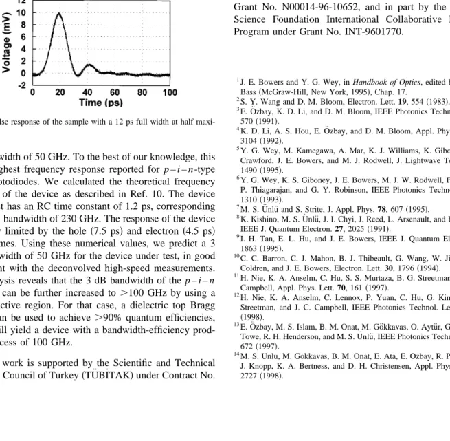
High-speed measurements were made with a picosecond Ti:sapphire laser operating at 820 nm. The 1.5 ps FWHM optical pulses from the laser were coupled into a single-mode fiber, and the other end of the fiber was placed in close proximity to the p – i – n photodiode by means of a probe station. Figure 3 shows the temporal response of a small area (7mm313mm) photodiode measured by a 50 GHz sampling scope. The measured photodiode output has a 12 ps FWHM. The Fourier transform of the data has a 3 dB bandwidth of 38 GHz. The measured data are corrected by deconvolving the scope response, which is assumed to be a Gaussian pulse with a 7 ps rise time. After this correction, the device has a 3
FIG. 1. Experimental and theoretical reflectance characteristics of the as-grown RCE p – i – n photodiode structure.
FIG. 2. ~a! Experimental and ~b! theoretical photoresponse characteristics of fabricated devices. Plot 1 corresponds to the as-grown sample, while plots 2–5 correspond to the characteristics after consecutive recess etches.
1073
dB bandwidth of 50 GHz. To the best of our knowledge, this is the highest frequency response reported for p – i – n-type RCE photodiodes. We calculated the theoretical frequency response of the device as described in Ref. 10. The device under test has an RC time constant of 1.2 ps, corresponding to a 3 dB bandwidth of 230 GHz. The response of the device is mostly limited by the hole ~7.5 ps! and electron ~4.5 ps! transit times. Using these numerical values, we predict a 3 dB bandwidth of 50 GHz for the device under test, in good agreement with the deconvolved high-speed measurements. Our analysis reveals that the 3 dB bandwidth of the p – i – n structure can be further increased to.100 GHz by using a thinner active region. For that case, a dielectric top Bragg mirror can be used to achieve .90% quantum efficiencies, which will yield a device with a bandwidth-efficiency prod-uct in excess of 100 GHz.
This work is supported by the Scientific and Technical Research Council of Turkey~TU¨BI˙TAK! under Contract No.
197-E044, in part by the Office of Naval Research under Grant No. N00014-96-10652, and in part by the National Science Foundation International Collaborative Research Program under Grant No. INT-9601770.
1J. E. Bowers and Y. G. Wey, in Handbook of Optics, edited by Michael Bass~McGraw-Hill, New York, 1995!, Chap. 17.
2
S. Y. Wang and D. M. Bloom, Electron. Lett. 19, 554~1983!.
3E. O¨ zbay, K. D. Li, and D. M. Bloom, IEEE Photonics Technol. Lett. 3, 570~1991!.
4K. D. Li, A. S. Hou, E. O¨ zbay, and D. M. Bloom, Appl. Phys. Lett. 61, 3104~1992!.
5Y. G. Wey, M. Kamegawa, A. Mar, K. J. Williams, K. Giboney, D. L. Crawford, J. E. Bowers, and M. J. Rodwell, J. Lightwave Technol. 13, 1490~1995!.
6
Y. G. Wey, K. S. Giboney, J. E. Bowers, M. J. W. Rodwell, P. Silvestre, P. Thiagarajan, and G. Y. Robinson, IEEE Photonics Technol. Lett. 5, 1310~1993!.
7M. S. U¨ nlu¨ and S. Strite, J. Appl. Phys. 78, 607 ~1995!.
8K. Kishino, M. S. U¨ nlu¨, J. I. Chyi, J. Reed, L. Arsenault, and H. Morkoc¸, IEEE J. Quantum Electron. 27, 2025~1991!.
9I. H. Tan, E. L. Hu, and J. E. Bowers, IEEE J. Quantum Electron. 31, 1863~1995!.
10C. C. Barron, C. J. Mahon, B. J. Thibeault, G. Wang, W. Jiang, L. A. Coldren, and J. E. Bowers, Electron. Lett. 30, 1796~1994!.
11
H. Nie, K. A. Anselm, C. Hu, S. S. Murtaza, B. G. Streetman, and J. C. Campbell, Appl. Phys. Lett. 70, 161~1997!.
12H. Nie, K. A. Anselm, C. Lennox, P. Yuan, C. Hu, G. Kinsey, B. G. Streetman, and J. C. Campbell, IEEE Photonics Technol. Lett. 10, 409
~1998!.
13
E. O¨ zbay, M. S. Islam, B. M. Onat, M. Go¨kkavas, O. Aytu¨r, G. Tuttle, E. Towe, R. H. Henderson, and M. S. U¨ nlu¨, IEEE Photonics Technol. Lett. 9, 672~1997!.
14M. S. Unlu, M. Gokkavas, B. M. Onat, E. Ata, E. Ozbay, R. P. Mirin, K. J. Knopp, K. A. Bertness, and D. H. Christensen, Appl. Phys. Lett. 72, 2727~1998!.
FIG. 3. Pulse response of the sample with a 12 ps full width at half maxi-mum.