Nanocrystal hybridized scintillators for
enhanced detection and imaging on Si platforms
in UV
Evren Mutlugun, Ibrahim Murat Soganci, and Hilmi Volkan Demir
Department of Physics, Department of Electrical and Electronics Engineering, Nanotechnology Research Center, Bilkent University, Bilkent, Ankara, Turkey 06800
Abstract: We report on the conception, design, fabrication, experimental characterization, and theoretical analysis of nanocrystal scintillators hybridized on Si detectors and CCDs for enhanced detection and imaging in UV. Integrating luminescent CdSe/ZnS core-shell nanocrystals (NCs of 3.2 and 5.2 nm in diameter with 5% size distribution) to efficiently convert incident UV radiation to visible emission, we demonstrate hybrid NC-Si photodetectors that exhibit significantly improved responsivity between 200-240nm, experimentally with a two orders of magnitude peak enhancement and theoretically with a three orders of magnitude peak enhancement. Such nanocrystal based scintillators hold great promise in UV detection and imaging on Si platforms.
©2007 Optical Society of America
OCIS codes: (250.0250) Optoelectronics; (260.7190) Ultraviolet; (160.2540) Fluorescent and
luminescent materials; (040.0040) Detectors; (040.6040) Silicon. References and links
1. L. Pavesi and D. J. Lockwood, Silicon Photonics (Springer, 2004).
2. G. T. Reed and A. P. Knights, Silicon Photonics: An Introduction (John Wiley and Sons, 2004). 3. R. Soref, “Silicon photonics technology: past, present, and future,” Proc. SPIE 5730, 19-28 (2005). 4. C. Gunn, “CMOS photonics for high-speed interconnects,” IEEE Micro 26, 58-66 (2006).
5. C. Gunn, “Photonics integration for optical interconnects,” in Proceedings of IEEE LEOS 2005 Annual Meeting (IEEE, 2005) pp. 732.
6. T. T. Saito, “Technological opportunities in homeland security,” http://www.coloradophotonics.org 7. T. Price, “Homeland security forces seek help from optical science,” Opt. Photonics News 16-17 (2006). 8. S. Gaponenko, Optical properties of semiconductor nanocrystals (Cambridge University Press, 1998). 9. M. A Hines, and P. Guyot-Sionnest, “Synthesis and characterization of strongly luminescent ZnS-capped CdSe
nanocrystals,” J. Phys. Chem. 100, 468-471 (1996).
10. B. O. Dabbousi, J. Rodriguez-Viejo, F. V. Mikulec, J. R. Heine, H. Mattoussi, R. Ober, K. F. Jensen and M. G. Bawendi, “(CdSe)ZnS core-shell quantum dots: synthesis and characterization of a size series of highly luminescent nanocrystallites,” J. Phys. Chem. B 101, 9463-9475 (1997).
11. S. Coe, W.-K. Woo, M. Bawendi, and V. Bulovic, “Electroluminescence from single monolayers of nanocrystals in molecular organic devices,” Nature 420, 800-803 (2002).
12. S. Chaudhary, M. Ozkan, and W. C. W. Chan, “Trilayer hybrid polymer-quantum dot light-emitting diodes,” Appl. Phys. Lett. 84, 2925-2927 (2004).
13. S. Nizamoglu, T. Ozel, E. Sari, and H. V. Demir, "White light generation using CdSe/ZnS core-shell nanocrystals hybridized with InGaN/GaN light emitting diodes," Nanotechnology 18, 065709 (2007). 14. J. Liu, T. Tanaka, K. Sivula, A. P. Alivisatos, and J. M. J. Fréchet, “Employing end-functional polythiophene to
control the morphology of nanocrystal-polymer composites in hybrid solar cells,” J. Am. Chem. Soc. 126, 6550-6551 (2004).
15. D. Qi, M. B. Fischbein, M. Drndic, and S. Selmic, “Efficient polymer-nanocrystal quantum-dot photodetectors,” Appl. Phys. Lett. 86, 093103 (2005).
16. M. B. Fischbein and M. Drndic, “CdSe nanocrystal quantum-dot memory,” Appl. Phys. Lett. 86, 193106 (2005).
17. H. V. Demir, I. M. Soganci, and E. Mutlugun, “CdSe/ZnS core-shell nanocrystal based scintillators for enhanced detection in UV,” in Proceedings of IEEE LEOS 2006 Annual Meeting (IEEE 2006), pp. WN3.
1. Introduction
Silicon photonics facilitates the ability to realize optoelectronic devices directly on very large-scale integrated electronic circuits [1-3]. This is critically important for optoelectronics to leverage advanced Si fabrication technology (e.g., Si CMOS and SOI) and its high computation power [4, 5]. However, Si material is constrained in different aspects for use in optoelectronics. Such one limitation is observed in Si based photodetectors and cameras that exhibit very poor responsivity in the ultraviolet (UV) spectral range. Consequently, Si photodetectors fabricated in standard CMOS process and Si CCD cameras cannot be utilized in UV detection and imaging, despite their advanced, low-cost, high-volume processing technologies. On the other hand, there exists a strong demand for UV detection and imaging, for instance in security applications [6, 7]. In this paper for the first time, we propose and demonstrate nanocrystal based scintillators hybridized on Si platforms to detect and image in the UV with significantly improved responsivity. Here we report on the conception, design, fabrication, experimental characterization, and theoretical analysis of CdSe based nanocrystal scintillators hybridized with Si detectors and CCDs.
Nanocrystals have attracted significant attention in recent years because of their extraordinary optical characteristics that arise from their three dimensional quantum confinement [8]. Nanocrystals that have radii smaller than the bulk exciton Bohr radius of the material feature discrete, atomic like energy levels. As a result, these nanocrystals exhibit ultra-narrow optical transitions, with high optical absorption levels and high quantum fluorescence efficiencies [9, 10]. Using the size effect, the optical absorption and emission spectra of the nanocrystals can further be conveniently tuned. These make nanocrystals attractive for use in different optoelectronic device applications including LEDs [11, 12], hybrid white light sources [13], photovoltaic cells [14], photodetectors [15] and optical memories [16]. However, the applications of nanocrystals are not limited only to such devices. In this work, we present a novel proof-of-concept scintillator that incorporates CdSe/ZnS core-shell nanocrystals to utilize both high optical absorption in the UV and high quantum fluorescence efficiency in the visible.
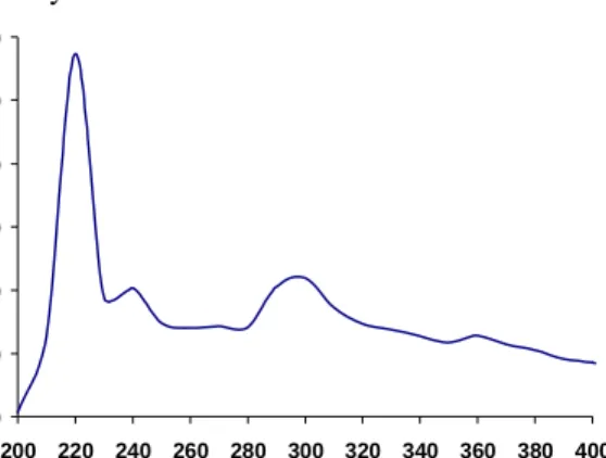
0 5000 10000 15000 20000 25000 30000 200 220 240 260 280 300 320 340 360 380 400 wavelength(nm) im p rovem ent (% )
Fig. 1. Experimental demonstration of improvement in the spectral response of a Si detector when hybridized with a nanocrystal scintillator (using red CdSe/ZnS nanocrystals).
In this work, we use luminescent CdSe/ZnS nanocrystals hybridized in a host polymer on the Si platform and obtain hybrid Si photodetectors that exhibit highly improved responsivity in the spectral range of 200-240 nm, experimentally with two orders of magnitude peak enhancement with respect to the host polymer film as shown in Fig. 1. Our nanocrystal based scintillators provide the ability to engineer the optical scintillation properties such as the enhancement spectral range and factor using different nanocrystal types, concentrations, and film thicknesses. Our theoretical modeling and experimental characterization show such nanocrystal integrated Si based hybrid systems hold great promise in UV detection and
imaging with their high orders of spectral responsivity improvement and adjustable properties as desired, also presenting market value for commercialization [17].
In our UV scintillators, we utilize nanocrystals for wavelength up-conversion in the processes of photodetection and imaging. There are three fundamental reasons for our choice of nanocrystals in this work: 1.) their high quantum fluorescence efficiency, 2.) their strong absorption, and 3.) the small overlap between their absorption and emission profiles (due to the quantum confinement). For nanocrystals with CdSe as the core and ZnS as the surrounding shell (providing surface passivation), the quantum fluorescence efficiency may increase as high as 60% across the visible spectral range at room temperature [8-10]. Also, the absorption coefficient of such nanocrystals may be very high (ten thousands of cm-1) at short wavelengths, covering the ultraviolet spectral range [8]. These properties make nanocrystals excellent candidates for the scintillator application as demonstrated in this letter.
2. Principle of operation and design of nanocrystal scintillators
The working principle of this scintillator relies on the absorption and emission spectra of the nanocrystals that are sufficiently separated from each other. As a result of the high absorption coefficient in the UV region, incident ultraviolet light creates electron-hole pairs with high efficiency, and the resulting recombination occurs at the emission wavelength in the visible range, which is longer than the absorption wavelength. Therefore, by hybridizing nanocrystals, for example, on a Si platform, it is possible to have otherwise undetectable UV photons to be converted to visible photons to be detected by the Si platform. Also, the emission wavelength of the nanocrystals may further be tuned to any desired point in the visible by simply changing the size of the nanocrystals as necessitated by the specification of the scintillator application. For even more efficient performance, the absorption and emission spectra of the nanocrystals may further be separated (e.g., through doping with Mn) to have minimum overlap and thus to minimize reabsorption of the emitted light in principle. In this work, we use conventional core-shell nanocrystals for proof-of-concept device demonstration.
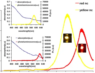
0 5000 10000 15000 20000 25000 30000 440 460 480 500 520 540 560 580 600 620 640 wavelength(nm) P L in te n s it y ( a .u ) red nc yellow nc 0 0.1 0.2 0.3 0.4 0.5 0.6 0.7 400 440 480 520 560 600 640 wavelength(nm) a b s o rp ti on( a .u) 0 10000 20000 30000 40000 50000 60000 70000 PL (a .u ) absorption(a.u) photoluminescence(a.u) 0 0.1 0.2 0.3 0.4 0.5 0.6 0.7 400 440 480 520 560 600 640 wavelength(nm) ab so rp ti o n (a .u ) 0 10000 20000 30000 40000 50000 60000 70000 PL ( a .u ) absorption(a.u) photoluminescence(a.u)
Fig. 2. Photoluminescence spectra of our red and yellow nanocrystals (NC). Insets show the absorption spectrum along with the photoluminescence spectrum of the respective nanocrystal.
Figure 2 shows the photoluminescence spectra of our scintillator CdSe/ZnS core-shell nanocrystals when pumped with He-Cd laser at 325 nm at room temperature. The inset shows the photoluminescence and absorption spectra of the respective nanocrystals. The absorption spectrum is obtained using UV-VIS spectrometer. These yellow and red CdSe/ZnS core-shell nanocrystals shown in Fig. 2 are 3.2 nm and 5.2 nm in diameter and exhibit emission peaks at
580 nm and 620 nm, respectively. They have a size distribution of ~5%. They feature quantum efficiencies around 10-20%. Due to the background absorption of host polymer, we typically use an optimal film thickness of 1.5 μm. We hybridize nanocrystals in host medium over Si platform using combinations of different processing techniques including chemical surface treatments, evaporation, spin-casting, and annealing. We design our nanocrystal scintillators using these two nanocrystal types with different concentrations and film thicknesses to investigate and compare the resulting scintillation properties.
3. Experimental characterization and theoretical analysis of nanocrystal scintillators The efficiency of our nanocrystal scintillators is determined by the excitation spectroscopy of the nanocrystals. Figure 3 shows the ratio of the emitted optical power to the incident optical power as a function of the excitation wavelength for red type nanocrystals in host polymer. Here we observe that this nanocrystal film is most efficiently pumped between 220 nm and 240 nm. This spectral response implies that the highest enhancement in responsivity is expected to occur in this wavelength range when this nanocrystal film is hybridized on a silicon platform. 0 2 4 6 8 10 12 14 16 18 2 0 2 0 0 2 2 0 2 4 0 2 6 0 2 8 0 3 0 0 3 2 0 3 4 0 3 6 0 3 8 0 4 0 0 W avelength (nm) P em it ted / P i n c ide nt ( % )
Fig. 3. The spectral ratio of the emitted optical power to the incident power measured on red type nanocrystals at room temperature.
Figure 4 shows the responsivity curves of a silicon detector with and without red nanocrystal hybridization (in red and navy curves, respectively), with the inset of Fig. 4 plotting the improvement in the spectral responsivity with respect to the bare Si detector. Here we observe that the responsivity of the bare silicon detector is improved with the use of nanocrystal scintillator in the entire spectrum except for a dip between 240 nm and 300 nm. This decrease in the effective responsivity stems from the host polymer that starts absorbing strongly below 300 nm. However, below 240 nm where Si detector exhibits very poor responsivity, the nanocrystals are much more efficiently pumped. Consequently, the effective responsivity is significantly improved between 200-240 nm, despite the increasing absorption level of host polymer. Here using this nanocrystal scintillator, we experimentally achieve effective responsivity in the range of a few milliAmperes/Watts in the spectral range of 200-240 nm.
0.0 0E + 00 5.0 0E - 03 1.0 0E - 02 1.5 0E - 02 2.0 0E - 02 2.5 0E - 02 3.0 0E - 02 3.5 0E - 02 4.0 0E - 02 20 0 220 2 40 26 0 280 3 00 320 3 40 36 0 38 0 400 wa vel en g th ( n m ) -100 100 300 500 200 250 300 350 400 wavelength(nm) im p rovem en t( % )
Fig. 4. The spectral responsivity of a Si photodetector with and without hybridizing red nanocrystal scintillator measured at room temperature. (The responsivity of bare Si detector is shown in navy curve and that of the same Si detector integrated with red nanocrystal scintillator is shown in red curve; the inset shows improvement of the spectral responsivity.)
Figure 5 characterizes the optical transmission through the red nanocrystal film as well as the host medium of the same thickness, proving strong absorption of the polymer medium. That is why the enhancement of responsivity due to the nanocrystals with respect to the host polymer is much higher, as depicted in Fig. 1. We experimentally observe that the improvement in the effective spectral response of the red nanocrystal hybridized Si detector is as high as two orders of magnitude around 220 nm in Fig. 1. This means that the host polymer can be further optimized for this application to achieve high enhancements.
0 10 20 30 40 50 60 70 80 90 200 220 240 260 280 300 320 340 360 380 400 wavelength(nm) tr an sm is s io n (% ) transmission of polymer transmission of nanocrystals in polymer
Fig. 5. Transmission spectra of red nanocrystals and host polymer measured at room temperature.
Figure 6 plots the simulation results of the red nanocrystal scintillator integrated on Si detector, parameterized with respect to the nanocrystal quantum efficiency. Using the semi-empirical data of absorption spectra of the nanocrystals and the host medium, this model simulates the net optical emission from the hybridized nanocrystal film and its effect on the responsivity of the integrating Si detector. As shown in Fig. 6 along with the experimental data, we theoretically expect enhancements in the spectral responsivity as high as three orders of magnitude, one order of magnitude higher than the experimental results, provided that high enough quantum efficiencies are achieved. In this work, the limited quantum efficiency of our
nanocrystals reduces the feasible enhancement to two orders of magnitude. This implies that there is much more room for improvement.
Fig. 6. Semi-empirical simulation results for the improvement in the spectral responsivity of the Si photodetector integrating with red nanocrystal scintillators.
Figure 7 shows the enhancement in the responsivity of the integrating Si detector when hybridized with yellow type nanocrystals this time as another implementation example (in navy curve for bare Si detector and in yellow curve for yellow nanocrystal hybridized Si detector). The yellow nanocrystal scintillator yields enhancement in the responsivity of the integrating Si detector with the same spectral behavior, as in the case of red nanocrystal scintillator shown in Fig. 4. Likewise, the responsivity is improved across the entire spectrum except for the dip in the range of 220-300 nm because of the absorption of the host polymer starting in the UV. However, below 220 nm, where the yellow nanocrystals start to be pumped much more efficiently, the responsivity is improved despite the increasing absorption of the host polymer. Here the yellow nanocrystals lead to improved responsivity at a shorter wavelength in the deep UV compared to red nanocrystals because of their shifted excitation behavior (due to the size effect).
0.00E+00 1.00E-02 2.00E-02 3.00E-02 4.00E-02 5.00E-02 6.00E-02 200 220 240 260 280 300 320 340 360 380 400 wavelength(nm) re spo n si v it y (A /W ) -100 0 100 200 300 400 500 200 250 300 350 400 wavelength(nm) imp rove m ent (%)
Fig. 7. The spectral responsivity of a Si photodetector with and without hybridizing yellow nanocrystal scintillator measured at room temperature. (The responsivity of bare Si detector is shown in navy curve and that of the same Si detector integrated with yellow nanocrystal scintillator is shown in yellow curve; the inset shows improvement of the spectral responsivity).
Figure 8 presents a number of snapshots from CCD cameras with and without hybridizing nanocrystal scintillators. Figure 8(a) shows the response of a CCD under broad UV illumination, whereas Fig. 8(b) shows the response under the identical experiment conditions when the same CCD is hybridized with a red nanocrystal scintillator. Here while the bare CCD gives no response as depicted in Fig. 8(a), it provides a signal in Fig. 8(b), due to the nanocrystal scintillator hybridization. Likewise Figs. 8(c) and 8(d) compare the CCD responses with and without nanocrystal scintillator, this time illuminating a UV optical beam. Again, while the bare CCD gives no signal in Fig. 8(c), the nanocrystal hybridized CCD shows the UV spot in Fig. 8(d). This preliminary characterization on CCDs shows that the nanocrystal scintillators hold promise for UV imaging on Si platforms.
a b
c d
Fig. 8. Snapshots taken from CCD cameras under UV illumination at room temperature: the response of a CCD (a) without and (b) with hybridizing nanocrystal scintillator under broad UV illumination; and the response of another CCD (c) without and (d) with the scintillator when a UV optical beam is incident.
4. Conclusion
In conclusion, in this work for the first time, we present the conception of nanocrystal based scintillators and demonstrate their proof-of-concept use in the enhancement of photodetection and imaging on a Si platform in the UV spectral range. We experimentally show significant improvement in the effective spectral responsivity of Si detectors with two orders of magnitude peak improvement in the UV, which is limited by the quantum efficiency of the nanocrystals and the background absorption of the host medium. We theoretically expect to achieve enhancement in the spectral responsivity as high as three orders of magnitude with sufficiently high nanocrystal quantum efficiencies and optimized host polymers. Our preliminary characterization also demonstrates the facilitation of Si CCD with hybridizing nanocrystal scintillators for possible imaging in UV. We conclude that the functionalization of Si platforms with such hybridizing nanocrystal scintillators finds applications in detection and imaging in the UV, presenting market value for commercialization.
Acknowledgment
This work is supported by EU-PHOREMOST Network of Excellence 511616 and Marie Curie European Reintegration Grant MOON 021391 within the 6th European Community Framework Program and TUBITAK under the Project Nos. 106E020, 104E114, 105E065, and 105E066. Also, HVD acknowledges additional support from the Turkish Academy of Sciences Distinguished Young Scientist Award (TUBA GEBIP) and IMS acknowledges TUBITAK Fellowship. The authors would further like to thank Dr. Aykutlu Dane and Turgut Tut for their strong support and fruitful discussions.