www.advopticalmat.de
Semiconductor Thin Film Based Metasurfaces and
Metamaterials for Photovoltaic and Photoelectrochemical
Water Splitting Applications
Amir Ghobadi, Turkan Gamze Ulusoy Ghobadi, Ferdi Karadas, and Ekmel Ozbay*
DOI: 10.1002/adom.201900028
throughput and large-scale compatibility. The photoactive material is generally com-posed of single or multiple semiconductor layers responsible for harvesting solar energy. This harvested solar irradiation can be used to generate electricity using photovoltaic (PV) devices, or it can be converted to chemical energy in the form of hydrogen which is the case for photo-electrochemical water splitting (PEC-WS). In both PV and PEC-WS applications, the ultimate goal is to establish an efficient photon capturing and electron collecting scheme to generate a huge number of photocarriers (including electron–hole pairs) with rational carrier dynamics (effi-cient charge generation, separation, and collection). This means that the device should be optically thick enough to gen-erate high carrier’s density and electrically thin enough to collect photogenerated carrier before they recombine. When light impinges a semiconductor surface, a part of the light is reflected back due to the mis-match between the air and the semicon-ductor layer refractive index. The rest will propagate within the bulk until it is fully absorbed by the semi-conductor slab. The optical penetration depth (LPD) is defined as the depth at which the incident power falls to 1/e (≈37%) of its input value. This parameter differs from one semiconductor to another and it depends on the extinction coefficient (κ) of the
In both photovoltaic (PV) and photoelectrochemical water splitting (PEC-WS) solar conversion devices, the ultimate aim is to design highly efficient, low cost, and large-scale compatible cells. To achieve this goal, the main step is the efficient coupling of light into active layer. This can be obtained in bulky semiconductor-based designs where the active layer thickness is larger than light penetration depth. However, most low-bandgap semiconductors have a carrier diffusion length much smaller than the light penetration depth. Thus, photogenerated electron–hole pairs will recombine within the semiconductor bulk. Therefore, an efficient design should fully harvest light in dimensions in the order of the carriers’ diffusion length to maximize their collection probability. For this aim, in recent years, many studies based on metasurfaces and metamaterials were conducted to obtain broadband and near-unity light absorption in subwavelength ultrathin semiconductor thicknesses. This review summarizes these strategies in five main categories: light trapping based on i) strong interference in planar multilayer cavities, ii) metal nanounits, iii) dielectric units, iv) designed semiconductor units, and v) trapping scaffolds. The review highlights recent studies in which an ultrathin active layer has been coupled to the above-mentioned trapping schemes to maximize the cell optical performance.
A. Ghobadi, Prof. E. Ozbay
NANOTAM—Nanotechnology Research Center Bilkent University
Ankara 06800, Turkey E-mail: [email protected] A. Ghobadi, Prof. E. Ozbay
Department of Electrical and Electronics Engineering Bilkent University
Ankara 06800, Turkey
T. G. Ulusoy Ghobadi, Prof. F. Karadas
UNAM—National Nanotechnology Research Center Institute of Materials Science and Nanotechnology Bilkent University
Ankara 06800, Turkey
Light Trapping
The ORCID identification number(s) for the author(s) of this article can be found under https://doi.org/10.1002/adom.201900028.
1. Introduction
The main goal in solar energy harvesting devices is to design a low-cost sustainable and efficient architecture as well as ele-mentally earth abundant materials to have high manufacturing
T. G. Ulusoy Ghobadi
Department of Energy Engineering Faculty of Engineering Ankara University Ankara 06830, Turkey Prof. F. Karadas Department of Chemistry Faculty of Science Bilkent University Ankara 06800, Turkey Prof. E. Ozbay Department of Physics Bilkent University Ankara 06800, Turkey
material (which is the imaginary part of the complex refractive index). The values of LPD are plotted in Figure 1a–c, for dif-ferent semiconductor materials at three difdif-ferent visible wave-lengths of λ = 400, 500, and 600 nm. As it can be deduced from these panels, to harvest the whole penetrated light, a minimal slab thickness of a couple hundred nanometers is required, for most of semiconductors. However, to maximize the car-rier collection capability of the design, the semiconductor layer should be thinner than the carrier diffusion length. The carrier diffusion length (LD) is the length that a carrier can transport without being recombined. LD is an inherent property of semi-conductor material and it mainly depends on the crystallinity phase of the layer. However, for most semiconductors, LD is much smaller than LPD. Thus, it is essential to propose a design architecture to absorb light in dimensions much smaller than the LPD. However, this cannot be satisfied using a con-ventional design in such thin layers. Absorption coefficient, α, cannot be improved using synergetic effects; it is an inherent property of material. However, this deficiency can be signifi-cantly suppressed by using light trapping nanostructures. This could be achieved using ultrathin semiconductor based metas-urface and metamaterial designs. Metamaterials refer to a class of synthetic materials comprising designed inclusions with exotic properties that cannot be attained using natural ones. The concept of light confinement and its harvesting using subwave-length architectures has been one of the most studied applica-tions of metamaterials. These designed architectures can go beyond the inherent limitations of conventional optoelectronic devices. Semiconductor nanostructuring is an efficient way to increase the light harvesting property of the material and many great reviews have already covered these design strategies in different optoelectronic applications.[1–5] Generally speaking, in this design strategy, the nanostructured surface will simultane-ously suppress light reflection and increase light coupling into the underlying bulk active layer. Thus, the above-mentioned architectures are generally bulky designs. For some of single-crystalline semiconductor materials such as Si or GaAs with LD values in the order of hundreds of micrometers, this is an efficient approach to maximize the photoconversion efficiency of the cell. However, for the most of semiconductors, the LD is much shorter than the LPD and therefore nanostructuring is the best solution. Even for semiconductors with large LD, this length is significantly shortened if we move to poly-crystalline or amorphous phases. Thus, for a wise design, it is of great importance to keep active layer thickness as thin as carrier’s diffusion length. Thus, this review will not cover those bulky nanostructuring ideas. The main motivation of this review is to find the strategies in which light perfect absorption can occur in thin active layer dimensions (rather than the bulk ones). This review will provide a comprehensive study on the design of effi-cient light harvesting devices using thin semiconductor layers. In other words, we will study how different 2D metasurface and 3D metamaterial-based trapping schemes can efficiently couple light into a thin semiconductor layer. Near perfect harvesting of solar irradiation in a broad spectral range in such thin semicon-ductor layer geometries could lead to the realization of highly efficient, cost effective, and large scale compatible PV and PEC-WS devices. In the following sections, we will categorize the different trapping schemes and scrutinize their use in light
Amir Ghobadi obtained his B.S. degree in electrical engi-neering from the University of Tehran, Iran in 2012. He obtained his M.S. degree from the same department at Bilkent University in 2014. Currently, he is working toward his Ph.D. under the supervision of Prof. Ekmel Ozbay at Bilkent University. His research involves the design, synthesis, and characterization of novel semicon-ductor-based optic and photonic devices.
Turkan Gamze Ulusoy Ghobadi received her B.S. degree in chemical engineering from Ankara University, Turkey in 2012. She joined the National Nanotechnology Research Center (UNAM), Institute of Materials Science and Nanotechnology, Bilkent University, Turkey and obtained an M.S. degree in 2015. Currently, she is pursuing her Ph.D. degree in the same department under the guidance of Asst. Prof. Ferdi Karadas from the Chemistry Department. She became a research assistant in the Department of Energy Engineering at Ankara University in 2017. Her current research interests focus on the development of (photo)electrochemical mate-rials for energy storage and conversion systems.
Ekmel Ozbay obtained M.S. and Ph.D. degrees in electrical engineering from Stanford University in 1989 and 1992, respectively. He worked as a postdoctoral research associate at Stanford University and as a scientist at Iowa State University. He joined Bilkent University (Ankara, Turkey) in 1995, where he is currently a full professor in the Physics Department and EEE Department. In 2003, he founded the Bilkent University Nanotechnology Research Center (NANOTAM) where he leads a research group working on nanophotonics, nanometamaterials, nanoelectronics, GaN/AlGaN MOCVD growth, and GaN based devices. Recently he became the CEO of a spin-off company: AB-MicroNano Inc. He has published 420+ arti-cles in SCI journals (with an SCI h-index of 70), including a Science paper on plasmonics.
harvesting devices. Finally, we will provide an outlook to high-light the future direction of these ultrathin metadesigns.
2. Light Trapping Schemes
2.1. Light Trapping Based on Strong Interference in Planar Multilayer Cavities
Strong interference in metal-lossy layer interface could provide the condition to obtain perfect light absorption in dimensions much smaller than the light wavelength. This phenomenon offers the opportunity to use planar lithography-free multilayer designs for ultrathin optoelectronic applications. These multi-layer resonant absorbers have been realized in different types of materials and spectral regions. The most common mate-rials for realization of light perfect absorption are metals. It was shown that the use of lossy metals such as Cr, in a metal– insulator–metal (MIM) configuration, can provide light perfect absorption from 450 to 850 nm.[6] This absorption can be further improved by introduction of an insulator layer on top of this cavity which acts as a broadband antireflective coating. The use of metal–insulator-metal–insulator (MIMI) configura-tion enhances the absorpconfigura-tion bandwidth (BW) toward longer wavelength values.[7,8] Different metal–insulator combinations were utilized to obtain ultrabroadband light absorption from these multilayer designs. W-Al2O3,[9] Cr-SiO2,[8] W-SiO2,[8] Mo-SiO2,[8] Ag-Si,[10] Bi-LiF,[11] and Ni-SiO2[12] are some exam-ples of these MI pairs to obtain perfect broadband absorption. Further improvements can be also achieved using different strategies; excitation of multiple modes in a multithickness absorbing layer,[13] reducing the effective permittivity of metals via their composition with air,[14,15] the optimal selection of materials to maximize absorption BW[16] are some examples of these strategies. A recent perspective by our group reviews
strong light-matter interaction in lithography-free planar per-fect absorbers.[17] It was shown, upon choice of proper material and configuration, this absorbing behavior can be realized in almost all parts of electromagnetic (EM) spectrum. Although the common materials for the design of multilayer absorber metasurfaces are metals, this strong interference can also be found in semiconductors in the photon energies above their optical bandgap.[18,19]
The simplest way to increase the absorption of an ultrathin semiconductor slab is to introduce a back-reflecting metal mirror. This metal layer reflects the light back into the slab and increases the optical path of the light inside the medium. If the impedance matching condition can be satisfied, we can trap the light inside the layer and fully harvest it in the resonance wave-length. This is called Fabry-Perot (FP) resonance. The spectral position of FP resonance in metal–semiconductor (MS) configu-ration is a function of semiconductor’s refractive index, extinction coefficient, and thickness. To gain insight on the ideal condition to obtain strong light absorption, the transfer matrix method (TMM) is utilized.[17,20,21] Using this modeling approach, the bottom layer is chosen as an optically thick metal layer. The bottom mirror is chosen as Al which has relatively flat high reflection throughout the whole visible range. Then, the ideal absorption region (absorption near unity or reflection near zero) is extracted for three different slab thicknesses (DS) of 3, 10, and 30 nm. The threshold for absorption is chosen as 0.8 (where reflection is below 0.2). It should be noted that the upper scale of the color bar have been set as 0.25 to provide a better visu-alization for the borders of 0.2 reflection. These ideal regions are compared with the refractive index (n) and extinction coefficient (k) data of typical semiconductors, as shown in Figure 2a–c. As depicted in these panels, the reflection counter plots are made of centric circles and being located inside this colored region means an absorption above 0.8 (reflection below 0.2). These ideal regions are extracted from three visible light Figure 1. The light penetration depth (LPD) for different types of semiconductors at three different wavelengths of a) 400 nm, b) 500 nm, and
wavelengths of 400, 500, and 600 nm. As shown in Figure 1a–c, the ideal circular patterns for a 3 nm thick layer is located at high n and k values that cannot be satisfied with common nat-ural semiconductors. Therefore, as can be deduced from these panels, none of the semiconductors are matched with this ideal region. By increasing the slab thickness to 10 and 30 nm, the ideal n, k circles shift toward smaller values but, in the mean-time, their radii get smaller. According to these contour plots, high refractive index semiconductors, such as germanium (Ge) and molybdenum disulfide (MoS2), can show strong interfer-ence at a relatively moderate thickness of 10 nm. However, other materials with smaller n and k values, such as oxides and organic semiconductors need a larger thickness to have strong absorption. For instance, Ge n and k data have located inside ideal region circles for a 10 nm thick layer in all three wave-lengths of 400, 500, and 600 nm. While for hematite (α-Fe2O3), this matching is achieved for a thicker layer of 30 nm. These findings are in line with previous studies. Kats et al. showed strong interface effects in an Au-Ge MS structure in which the spectral position of reflection dip is tuned by Ge thickness.[19] It has been proven later on that this MS configuration can go beyond the Yablonovitch limit.[22] This strong absorption has been also detected in a couple of tens of nanometer thick MoS2 layer on top of Au/Ag mirror.[23] Later, a proof-of-concept device has been made to reveal the potential of ultrathin transition metal dichalcogenides (TMDs) for energy conversion applica-tions.[24] A 22 nm thick Fe
2O3 on Ag mirror has also been shown to have strong light absorption at λ < 450 nm.[25] Similar optical responses have been realized for another type of metals
and semiconductors.[26,27] This strong interference is not only probed in semiconductor based cavity designs but also exci-tonic thin films, such as dyes and organic molecules, and could also show light perfect absorption.[28,29] The optical response of these organic materials (n and k values) can be controlled with the change in the aggregate concentration. Thus, the optical response of the cavity can be easily tailored. It should be men-tioned that the use of lossy metals as the reflector layer could make this interference effects stronger. This has been studied for many different MS configurations, specifically for color filter applications.[26,27,30] It was shown that an ultrathin Si layer on different metal types, such as Au, Ag, Cr, and Ti, has quite different absorption responses. In general, the low loss metals, such as Au, Ag, and Al, provide perfect absorption condition in a relatively narrow spectral range while lossy ones offer a broad absorption BW. However, when it comes to photovoltaic and photochemistry, our goal is to maximize absorption in the sem-iconductor layer (rather than the back metal). Therefore, the use of low loss highly reflective metals, such as Au, Ag, and Al, is desired. Moreover, the main goal in the design of an efficient semiconductor based metasurface is to achieve near unity absorption in the thinnest possible layer and broadest wave-length regime. This could be achieved by the introduction of metal–oxide–semiconductor (MOS) configuration. The spacer layer, which is the transparent oxide layer in the MOS configu-ration, can be counted as a new parameter to tune the absorp-tion strength and BW of the metasurface design. Similar to the case of MS configuration, the ideal regions have been extracted for the case of MOS cavity (Figure 2d–f). The spacer layer is set Figure 2. The reflection contour plot for an MS cavity design at three different wavelength values of a) 400 nm, b) 500 nm, and c) 600 nm. d–f) Similar
plot for an MOS junction with a TiO2 spacer layer of 20 nm. In all of the panels, the largest circle belongs to a DS of 3 nm, the middle one is for 10 nm, and the smallest circle is the ideal data for 30 nm thick ideal absorber. These ideal n and k regions are compared with those of typical visible active semiconductors.
as titanium dioxide (TiO2) with a thickness of 20 nm, which is much smaller than the incident visible light wavelength and, consequently, it could make a destructive interference between the electromagnetic fields at the top surface to trap the incident light. Compared to MS configuration, embedding a transparent oxide between metal and semiconductor coatings can shift the ideal absorbing region toward smaller refractive index values. Moreover, the circle sizes become larger and this in turn enhances the probability of matching between the ideal area and the semiconductor refractive index data. As we can see in Figure 2d–f, unlike MS cavity design, MOS configuration can provide strong light-matter interaction in thicknesses as thin as 3 nm. The matching is retained for 3 nm thick Ge in all three different wavelengths. This is in agreement with the experi-mental findings of an earlier study where the authors improved the absorption BW and strength by the introduction of a silicon dioxide (SiO2) transparent oxide between Au and Ge layers.[31] As already explained, the oxide layer with a thickness much smaller than the incident light wavelength can broaden the absorption BW. In the meantime, thicker spacer layers could offer a quarter wavelength matching condition. In this case, the destructive interference only occurs in a narrow wavelength range and this can be used to obtain spectrally selective light absorption. A recent study demonstrated the realization of effi-cient and ultrathin MOS cavities based on single crystalline Ge for spectrally selective photodetector applications.[32] This strong light-matter interaction for an MOS design is specifically important for 2D semiconductors, such as TMDs. That is because the excitonic response of these materials is improved as they are thinned down to atomic levels. While 3 nm thick MoS2 (which corresponds two an approximately five-layer thick) has weak matching condition with the ideal region in the MS configuration, its utilization in an MOS configuration can lead to nearly perfect absorption in both 400 and 500 nm incident lights. It has been shown that an Ag-MgF2-(four-layer) MoS2 cavity can have near unity absorption from 550 up to 700 nm.[33] A similar functionality has been also found in other type of semiconductors such as hematite. The optimal thickness for this material in an MOS cavity configuration is found to be 10 nm, which is much thinner compared to the optimum thick-ness of 30 nm for MS case. It should be noted that another resonant configuration is based on metal–semiconductor–oxide (MSO) design. In this architecture, the top oxide layer acts as an antireflective (AR) coating to match the air impedance into underneath the MS cavity. Based on the thickness and refrac-tive index of this AR coating, one could obtain broad or narrow absorption peak. This has been explored in a previous study for the case of Ge and the monolayer of MoS2.[34,35] Therefore, all of these aforementioned theoretical findings can be viewed from two main perspectives; first, the MOS structure, with one more degree of freedom, could be designed in a way to obtain a stronger and broader absorption response that is necessary for energy conversion applications. Second, the absorption of light in thinner semiconductor thicknesses (as in the case of MOS cavity) could promote the collection probability of the carriers. As an instance, the main limiting factor for α-Fe2O3 based water splitting photoanodes is their short hole diffusion length (below 20 nm).[36] Therefore, the absorption of the light in dimensions smaller than this thickness could significantly
enhance photogenerated holes participation in water oxidation reaction. In addition, this oxide layer could act as an electron (or hole) transport layer. The proper band alignment at the interface of the top semiconductor and the oxide spacer can spatially separate carriers and consequently prolong their life-time. This ultrathin spacer layer has also been found to enhance the efficiency of the organic solar cells by its simultaneous role in improving the electrical and optical behavior of the cell.[37]
Similar to the former design, a part of the incident light power can be consumed in the metal layer. This could be miti-gated by using photonic crystal (PC) based back reflector. A PC is made of an alternative arrangement of lossless high and low index transparent multilayers. This architecture has been used as the mirror layer to maximize the light absorption inside the semiconductor slab.[38,39] However, this is not the only way to use PCs for efficient light trapping. With such a hybrid multi-layer structure, optical Tamm resonance (which is also called surface state) can be excited near the PC and absorbing layer interface.[40] The intense Tamm resonance modes can bring a strong field localization to the incident photon energy, enabling light perfect absorption in sub-nanometer thick semiconductor layers. This design has been intensively employed for 2D semi-conductors, such as TMDs. It was found that a 1D PC on top of an MoS2 monolayer, with a back reflecting mirror, can effi-ciently couple the incident light into MoS2 monolayer within a narrow wavelength range.[41] The coupled field is harvested by MoS2 layer with an amplitude as high as 96%. The use of finite all-dielectric random PC has also been proven to pro-vide strong field localization which enables about 99.9% light perfect absorption by MoS2 monolayer in its resonance wave-length, due to Anderson localization.[42] As already proven, in the theoretical section, both MS and MOS junctions cannot satisfy the strong interference effects for semiconductor thick-nesses as thin as a monolayer TMD. In other words, realization of light perfect absorption in single TMD layer is not possible using these design cavities. Therefore, for the application of 2D PV and photodetection, the use of PC based design architec-ture could be of great interest. However, PC designs operate in a narrow spectral range and a broadening in the absorp-tion BW of the design is required to maximize the utilizaabsorp-tion of solar spectrum. A photodetector based on the monolayer of MoS2 embedded in chirped Bragg reflectors exhibit broad-band coherent light absorption that can harvest 33% of inci-dent visible light over a 300 nm BW.[43] Wu and co-workers have theoretically demonstrated a broadband near unity light absorption, covering the whole visible range, in a graphene-monolayer MoS2 photovoltaic cell.[44] The absorbing monolayer is located inside a wedge-shaped microcavity with a spectrum-splitting. Although this PC based design can be envisioned as a promising strategy to maximize 2D photovoltaic efficiency, it has a complex fabrication route due to the required multiple processing steps. At the expense of losing the absorption strength, a more feasible way was recently proposed where this atomically thin double layer cell is placed inside a metal-based wedge-shape cavity.[45]
Employing these simple resonant designs, other innovative planar and lithography-free structures have been utilized for PV and PEC-WS applications. In one of the pioneer studies, it was proven that a predesigned cavity with an impedance
match reflector can significantly enhance light absorption in the ultrathin α-Fe2O3 layer.[46] Employing this design strategy, a 71% above bandgap absorption can be attained in a layer as thin as 50 nm. The authors substantiated the photoresponse of the cell by Ti doping. Atomic layer deposition (ALD) of 25 nm thick α-Fe2O3 on Pt substrate with a thin TiO2 protection layer has been also demonstrated as an ultrathin efficient photoanode.[47] It was found that the proposed design can have a photo current density as high as 1.014 mA cm−2 at 1.4 V (vs RHE) and a max-imum external quantum efficiency (EQE) of 20.1% at 370 nm for an applied bias of 1.23 VRHE. Similar performance enhance-ment was recorded for an Au-Fe2O3 heterostructure.[48] A most recent paper proved an efficient design based on PC mirror in 10 nm thick α-Fe2O3 based MOS cavity. The proposed multi-layer structure is depicted in Figure 3a.[49] In this study, the authors were able to obtain highly efficient PEC-WS photo-anode using an active layer dimensions smaller than the hole diffusion length. To further improve the activity of the design, two photoanodes were placed face to face with an angle of 90°, as shown in Figure 3b, to harvest incident light as strongly as possible. In this case, the optical path of the light is signifi-cantly increased and more photons are captured. A substantial improvement was also achieved by introducing a cocatalyst on top of the active layer. The photocurrent spectra for all the dif-ferent design configurations have been depicted in Figure 3c. As this figure implies, the use of bottom PC mirror has increased the photocurrent of reference bare sample, mainly in the plateau region (at 1.6 VRHE). Adding the cocatalyst has improved both photocurrent value and shifts the onset poten-tial by 130 mV. Finally, combination of PC mirror, cocatalyst, and wedge configuration has increased the photocurrent by an order larger than two (compared to reference cell) at 1.6 VRHE.
This improvement is as high as four folds at the reversible potential of water oxidation, 1.23 VRHE. Apart from ALD and other similar processes that are conducted in low temperatures, the common fabrication route for narrow bandgap oxide semi-conductors involves a high temperature process to improve layer crystallinity.[50] For instance, the annealing temperature for α-Fe2O3 is typically around 800 °C which is close to the melting point of most noble metals. Therefore, the specular reflectivity of the bottom mirror can be diminished during this annealing step. Recently, a film flip and transfer process was adopted to enable the deposition of bottom mirror after the annealing process.[51] This process has been schematically depicted in Figure 4a. Similar to the above-mentioned study, homogeneous Ti doping was employed to further improve the electrical prop-erties of the α-Fe2O3 layer. As shown in the Figure 4b,c, the BW of the spectral region with near zero reflection is widened as we increase the α-Fe2O3 layer thickness. This is in line with our theoretical findings in Figure 2. Moreover, as these panels imply, the adding of cocatalyst does not significantly change the absorption property of the design. While the theoretical results estimated the highest absorption in a 20 nm thick semicon-ductor layer, the highest photocurrent values were obtained for an 8 nm thick layer, see Figure 4b. This was mainly due to the short hole diffusion length of the hematite layer where photo-carriers generated far from the surface cannot participate in the water oxidation process. The response was gradually improved by adding a cocatalyst into the system. This deficiency was fur-ther lessened by heterogeneous doping with the 1 cat% Zn— undoped—1 cat% Ti profile (cat.; cation fraction). As shown in Figure 4c, this modification led to a 1.01 mA cm−2 photocurrent in reversible potential of water oxidation (1.23 V vs RHE) for a 14 nm thick active layer. The Spalling process has also been Figure 3. a) Schematic representation of the proposed PC based photoanode. b) The 90° V-shaped cell configuration for enhancing light absorption. c) The Photocurrent voltammograms of photoanodes in planar configuration (red), with PC mirror in planar configuration (green), with PC mirror and cocatalyst overlayer in planar configuration (cyan), and two photoanodes with PC mirror and cocatalyst overlayer facing each other in the 90° V-shaped cell configuration. Reproduced with permission.[49] Copyright 2018, American Chemical Society.
demonstrated as an efficient way to make metal backed single crystalline ultrathin semiconductor layers. The use of Si and GaAs, as single crystalline semiconductor layers, in this con-figuration could offer a high efficiency photocathode.[52]
A similar story can be followed for these impedance matching metasurfaces in PV applications. In an earlier study on the application of these resonant designs in PV, a 13 nm thick amorphous germanium (a-Ge) layer was sandwiched between two ultrathin n- and p-doped amorphous silicon (a-Si) coatings,[53] see Figure 5a. As can be clearly seen in Figure 5b, it was found that the conversion efficiency in such an ultrathin solar cell design can be as high as 3.6%. Considering the small k values for the silicon layer (compared to its refractive index n) in the visible range, this configuration can be considered as an MOS cavity that has been capped with an AR coating (a-Si/ TCO/glass). Therefore, based on our theoretical findings, the strong interference is achieved in a specific active layer thick-ness. Simulated EQE data reveals that the optimal a-Ge layer thickness of 15 nm can provide an EQE of ≈80% in a broad range of 500–800 nm, see Figure 5c. The experimental data also show a maximum EQE of 60% at around 600 nm wavelength (Figure 5d). Another common semiconductor material for PV
applications is a-Si that has a compatible fabrication route for both MS and MOS configurations. A typical high efficiency a-Si based solar cell has an active layer thickness of 100–300 nm. However, the carrier diffusion length is much smaller than this thickness that makes the carrier collection efficiency low. There-fore, squeezing light absorption in dimensions as thin as the carrier’s diffusion length could be a prominent feature for the design of high-performance solar cells. Moreover, unlike thick a-Si based solar cells that have a dark appearance, these MS pairs based metasurface designs can act as reflective or transmissive color filters. This is highly desired for decorative purposes in both interior and exterior architectural features. However, based on the findings of previous studies, visible range reso-nant a-Si based color filters require a semiconductor thick-ness smaller than 25 nm.[54] This brings up a new challenge because it is known that the typical a-Si solar cell doping layers alone already impose an equivalent thickness in the range of 40–50 nm.[55] Therefore, a colorful a-Si based solar cell should have an ultrathin nonsilicon electron and hole transport layers. Lee et al. proposed a colored ultrathin solar cell that is made of a 10 nm–27 nm thick Si sandwiched between a 10 nm indene-C60 bisadduct (ICBA) electron transport layer, and 8 nm V2O5 Figure 4. a) The steps to fabricate Hematite based MOS cavity, b,c) the reflection spectra for MS cavities with different Hematite layer thicknesses,
and d,e) the photocurrent values of the photoanode for different semiconductor layer thicknesses and doping conditions. Reproduced with permis-sion.[51] Copyright 2018, Wiley-VCH.
hole extraction coating.[56] This three-layer design has been cov-ered with a thick (120 nm) bottom Ag layer (which acts as the bottom contact) and a semitransparent 23 nm top contact Ag. Therefore, the overall system can act as a colorful solar cell. By fixing the active a-Si layer thickness at 10, 18, and 27 nm, yellow, magenta, and cyan colors were accomplished. The highest overall efficiency of this ultrathin design was found to be 3%, which belongs to magenta. The maximum measured EQE values were found as 70%, 65%, and 40% for yellow, magenta, and cyan samples. While the above-mentioned conversion effi-ciencies and amorphous cell are quite remarkable, they are still much lower than the current state of the art for other similar types of thin film solar cells (e.g., 10% for a-Si).[57] This could be due to the narrow absorption spectra of the design. Moreover, although the thickness has been thinned down to a level com-parable with the carrier’s diffusion length, the crystallinity in such a thin layer is still a major challenge. Generally speaking, for a covalently bonded, isotropic semiconductor, reducing the thickness to the sub-100 nm range will cause significant dimin-ishing in crystalline quality, increasing in defect and disorder trap states and so on. Thus, amorphous based solar cells have generally shorter carrier diffusion length compared to single-crystalline ones. This in turn induces an inherent limit in the performance of ultrathin amorphous based semiconductor designs. A recent study demonstrated a fabrication route for a sub-10 nm single crystalline Ge layer for photodetection appli-cation.[32] The authors claimed that this approach can also be adopted for other type of semiconductors. However, a more
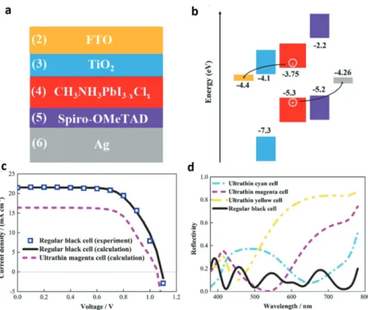
feasible route to realize an ultrathin single crystalline layer can be found in chemically synthesized highly absorbing organic layers. In a very recent study, Liu et al. demonstrated a magenta solar cell using a 30 nm thick perovskite (CH3NH3PbI3−xClx) showing remarkable efficiency as high as 11.5%.[58] The pro-posed colored solar cell design with its corresponding band alignments and J–V characteristics are depicted in Figure 6a–c. The obtained efficiency for this colorful solar cell design is 75% of that of the black thick cell (with a thickness an order of magnitude larger), which highlights the promising potential of metasurface design for colorful and efficient organic based solar cells. These results can be understood by looking at the reflection spectra of thick black cell and colored cells, Figure 6d. While the black cell has a broad and strong absorption from 400 to 800 nm, the magenta cell also depicts a strong absorption up to 650 nm. However, yellow and cyan samples have narrow absorption BW and consequently much less efficiency com-pared to black cell. As already stated, requiring colored behavior will sacrifice the absorption BW and this is one of the reasons that limits the efficiency of nanocavity based solar cells. A way to tackle this problem is to cascade multiple cavities in a proper way to have double resonant behavior and broaden the absorp-tion response. An elegant design made of an organic active layer was proposed by Liu and co-workers where they provide two-resonance cascaded cavities for broadband light trapping in thin-film organic solar cells, see Figure 7a. It was stated that the proposed design has the highest reported efficiency of 11.1% for an organic solar cell design,[59] see Figure 7b. The proposed Figure 5. a) The resonant cavity based ultrathin solar cell design, and b) its current–voltage characteristic showing a photoconversion efficiency of
3.6%. c) The simulated EQE for different a-Ge layer thicknesses, and d) a comparison between simulation and measurement EQE data for a 13 nm thick a-Ge layer based solar cell. Reproduced with permission.[53] Copyright 2015, Wiley-VCH.
structure has an EQE as high as 80% from 550 to 750 nm. Thus, it is envisioned that lithography-free planar metasurface designs incorporating ultrathin highly crystalline layers could
be promising options for future PV and PEC-WS applications. The proposed cavity has not only application in PV and PEC-WS, but also it can be utilized for emission applications. It is Figure 6. a) The proposed colored perovskite based solar cell design with its corresponding b) band alignments and c) J–V characteristics. d) The
reflection spectra for regular thick black cell and its comparison with colored ultrathin cyan, magenta, and yellow cells. Reproduced with permission.[58] Copyright 2018, Wiley-VCH.
Figure 7. a) Cascaded cavity based organic solar cell and b) its current–voltage characteristic under solar irradiation. Reproduced with permission.[59] Copyright 2017, Wiley-VCH.
known that reducing the size of a semiconductor nanoparticle down to its excitonic Bohr radius can intensify its emission property.[60,61] In the other side, as demonstrated in this paper, the strong light-matter interaction in a semiconductor based cavity occurs in nanometer scale thicknesses. Therefore, it is envisioned that introduction of a thin layer of semiconductor nanoparticles into this cavity can significantly enhance its emis-sion property. Chemical synthesis, chemical vapor deposition of 2D semiconductors (such as TMDs), and other innovative prep-aration and transfer routes can lead to substantial enhancement in the performance of these ultrathin optoelectronic designs. A further enhancement in the performance of these designs can be achieved by using ultrathin surface engineering where the electrical response is improved significantly while the optical response stays intact.[62–64]
2.2. Light Trapping Using Metal Nanounits
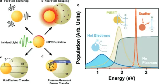
Upon the excitation of localized surface plasmons in metal– semiconductor interface, its energy can be transferred to the adjacent semiconductor via two main pathways; 1) radiative and 2) nonradiative energy transfer.[65] In the radiative energy process, the subwavelength metal particle acts like an antenna where excited hot electrons relax into lower energy states and reradiate as a secondary source. Keeping the antenna termi-nology in mind, this reradiated power can be coupled to the outside environment through propagating far field waves or it can be coupled to near field evanescent modes. The first process is called scattering and it is dominant in nanosphere diameters larger than 100 nm.[66] It should be noted that this property can be tuned by the refractive index of surrounding medium, com-position, and the wavelength. Scattering could be found in both metal and dielectric nanostructures and it mainly improves light trapping by maximizing the optical path of the light within the semiconductor.[65] The second process is named near
field coupling and it takes the main role in the energy transfer process for smaller plasmonic particles. This process imposes high field localization in the vicinity of metal particle where a high density of electron and hole pairs can be generated. But both of these processes can only intensify absorption in photon energies above the bandgap of the semiconductor. In other words, this process is to maximize the above bandgap absorp-tion of the design. Sub-bandgap absorpabsorp-tion could be achieved through nonradiative energy transfer routes. In this type of energy transfer, the plasmonic nanounit design contributes to enhancement in photocurrent by the direct injection of excited hot electron into the conduction band of the semiconductor. This mechanism is called hot electron injection. Upon irradia-tion of the metal–semiconductor juncirradia-tion, the localized surface plasmon resonance (LSPR) gets excited. The nonradiative decay of these LSPRs will generate hot electrons.[65] Most of these hot electrons have energetic location close to the metal Fermi level (Ef) and just a small portion of them can have required energy to overcome the Schottky barrier at the metal–semicon-ductor interface and contribute to the overall photocurrent.[67] Another nonradiative path is defined as plasmon-induced resonance energy transfer (PRET or PIRET). In this transfer mechanism, LSPR decay generates photocarriers directly in the semiconductor via dipole-dipole interactions with a tran-sient exciton.[68] The energetic overlap among plasmonic metal and semiconductor bands measures the overall efficiency of the process. All of these mechanisms have been schematically depicted in Figure 8a.[66] Based on the type of plasmonic metals, geometry of the design, including its size, shape, and composi-tion, and the nature of metal–semiconductor junccomposi-tion, some of these mechanisms can be activated or even dominant. A recent theoretical study has scrutinized the involved energy transfer processes in the plasmonic metal–semiconductor interface for photoconversion devices.[69] It has been demonstrated that in each of the plasmon energy levels (above, near edge, and below bandgap) a specific energy transfer mechanism is dominant.
Figure 8. Upon the excitation of plasmonic in metal–semiconductor interface, its energy can be transferred to the adjacent semiconductor via a)
far-field scattering, b) near-far-field coupling, c) hot-electron transfer, and d) plasmon resonant energy transfer. e) Schematic representation for where each plasmonic mechanism can lead to the largest enhancement in semiconductor photoconversion. a–d) Reproduced with permission.[66] Copyright 2016, Royal Society of Chemistry. e) Reproduced with permission.[69] Copyright 2015, Royal Society of Chemistry.
Scattering is the most efficient process in plasmon energy values larger than the semiconductor optical band edge, see Figure 8b. This is in line with our previous explanations that scattering could only provide absorption in above bandgap photons. The situation is the opposite for hot electron injection case. Theoretical findings predict their maximum contribution in photoconversion when bandgap is large (UV range) and the plasmon energy is below this bandgap. Although this process can open up the opportunity to use sub-bandgap photons, it has lower efficiency compared to scattering.[69] At the band edge or energy levels close to it, the PIRET process takes the dominant role. In this section, we will summarize the main strategies for enhancing light-matter interaction in a plasmonic metal– ultrathin semiconductor system. In this review, we focus on strategies for enhancement in the absorption capability of the semiconductor layer and, therefore, we will mainly consider the radiative energy transfer process rather than nonradiative ones. In other words, the motivation in this section is to highlight the trapping strategies based metal nanounits to efficiently couple the light into thin semiconductor active layers.
2.2.1. Plasmonic Nanoantennas
In ultrathin active semiconductor-based systems, to obtain strong light absorption, the optical path length of the incident plane wave should be maximized. This could be obtained by utilizing the scattering property of large metal nanoparticles. The scattering cross section of these metallic nanoparticles can be tuned by particles’ type, shape, size, distance from the semiconductor and the surrounding environment per-mittivity.[65] For instance, it has been found that cylindrical Ag particles can scatter a higher fraction of indent light into the underlying active layer compared to spherical shapes.[70] However, from the synthetic point, spheres are more fea-sible designs to be fabricated. Similarly, it was shown that the spectral position of maximum scattering experiences a red shift when the particle is brought to a contact with a high refractive index medium such as Si.[71] Considering the fact that most semiconductors have small k values in long wave-length visible and NIR ranges, this is quite desired to put this trapping mechanism in longer λs to enhance their weak inherent response. The optimum particle size for light scat-tering into the active layer is about ≈100 nm.[66] It should be noted that larger particles will suffer from high reflection and consequently less incident power will be accessible by active layer (specifically in shorter wavelengths where particle size is comparable with the incident light wavelength). Wrapping an ultrathin dielectric shell on plasmonic nanoparticle can further increase the scattering cross section of the design.[72] From the PV application perspective, this is also a beneficiary for suppressing recombination pathways. These metallic par-ticles, placed inside the bulk or the surface of semiconductor layer, could act as an undesired trapping center. While the use of a high bandgap oxide layer can electronically isolate them from the surrounding active area. Moreover, scattering which is also called light trapping can be more effective by the introduction of a metallic back mirror. By this way, light will transport longer distances within the semiconductor layer. In
addition, an intense localized field around a plasmonic object or at the metal–semiconductor interface can substantiate the density of generated electron–hole pairs.[73] These highly confined field regions are also referred as hot spots. These phenomena are mostly seen in deep subwavelength particle dimensions. These intense fields are not only for absorption enhancement, but they can also facilitate carrier separation at the metal–semiconductor interface by providing electric forces at the space charge region. Similar to scattering, near field coupling of these metallic nanoparticles depends on the geometrical parameters and the materials.[74] The hot spots are generally formed in nanounits with sharp corners.[75,76] Moreover, ultranarrow metallic gaps are favorable for the crea-tion of these intense local fields.[73] Thus, taking everything into account, these plasmonic nanoantennas can significantly boost semiconductor absorption capacity by either far-field scattering or near-field confinement. In the same time, they can improve the electrical behavior of the cell by improving the carrier separation dynamics.
One of the most prominent factors, defining the effective-ness of using plasmonics in energy conversion applications, is the position of this plasmonic particle in respect to the semi-conductor active layer. The initial attempts in this field proposed a configuration in which plasmonic particles are dispersed on top of the cell. Back in 1996, Stuart and co-workers proved the absorption enhancement upon coating them with metallic nano particles.[77] Later studies were conducted to enhance the efficiency of bulk solar cells by these plasmonic objects. How-ever, as already mentioned, plasmon induced optical and carrier dynamics improvement is much more pronounced in ultrathin active coatings. In 2006, in one of the pioneer studies, Derkacs et al. used silver nanoparticles in a-Si based solar cell to enhance light absorption and consequently overall conversion efficiency of the solar cell.[78] In this architecture, the plasmonic particles are placed on top of the solar cell, separated with a 20 nm thick indium tin oxide (ITO) conductive coating. Later on, this improvement was recorded for GaAs based PV cells.[79] Similar strategy has also been used for Cu(In,Ga)Se2 (CIGS) based thin solar cell to improve the photovoltaic performance of the design.[80] The use of these plasmonic particles in both front and back sides of ultrathin a-Si based solar cell has been also studied.[81] It was found that the particles at the backside have little to no impact on the device efficiency while the front parti-cles could improve light absorption. However, as stated herein-above, a part of performance improvement in plasmonic based systems comes from near field coupling. Therefore, it is envi-sioned that embedding particles within the bulk of the cell could provide a better performance improvement. This has been proved in the case of Ag and Au nanoparticles embedded in an ultrathin Si layer.[82,83] This is also beneficiary in terms of the long-term stability of the design where a lack of contact with air can minimize the formation of native oxide especially in the case of noble metals such Ag, Al, and Cu which have been found as promising and cost-effective alternatives for precious Au metal. This requirement is much more prominent in the case of water splitting where metals could easy undergo corro-sion upon their exposure to the water.[84] Koren et al. studied the impact of Au nanoparticles position relative to a semicon-ductor layer.[85] Their findings showed that Au nanoparticles on
the surface of the Fe2O3 active layer experience a redox reaction (Au + 3OH− ⇌ Au(OH)
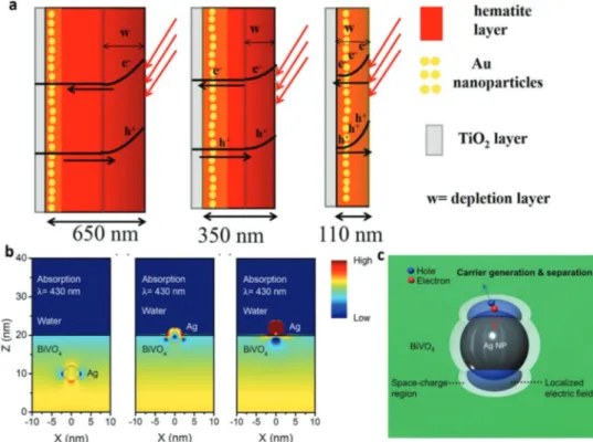
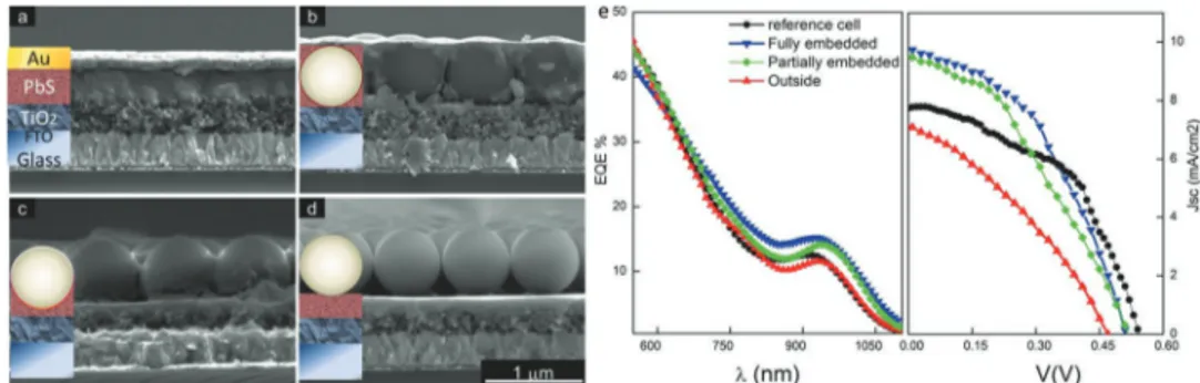
3 + 3e−) that gives rise to a spurious con-tribution to the current. In a second configuration, where the semiconductor layer has covered dewetted gold nanoparticles, the improvement and photocurrent-voltage characteristics were improved better. Although the second architecture enhanced the absorption capability of the design but wrapping Au monic particles with a high permittivity medium put the plas-monic resonance at 600 nm which is above the Fe2O3 band edge. Thus, they concluded that Mie scattering is the dominant process in the absorption enhancement. Their photocurrent improvement was more pronounced in lower applied voltages and almost no difference in larger bias values. They concluded that their activity enhancement is not only due to optical perfor-mance, but electrochemical effects are also present and effec-tive in an Au nanoparticle embedded design. Similar results were also found for the case of Au nanorod coated α-Fe2O3.[86] While redox reaction related peaks were also present in this case, but the photoactivity of semiconductor film was reinforced by Au nanoparticles. This improvement was negligible for thick layers (≈100 nm) while it was quite distinguishable for thin coatings (≈10 nm). Therefore, an elegant design should have plasmonics particles embedded within ultrathin film thicknesses. Archana and co-workers examined the impact of semiconductor hematite layer thickness on the photoactivity of the plasmonic incorporated photoanode.[87] Figure 9a shows the impact of hematite layer thickness in band alignment and the carrier concentration density of the design. In the 110 nm case, due to near-field coupling and Mie scattering, a greater density of photocarriers can be generated. Thus, in such a thin
thickness, the whole thickness is effectively depleted. However, as we go toward thicker layers, a larger amount of incident light will be consumed by semiconductor bulk and less will be cou-pled to Au nanoparticles. Moreover, considering the short diffu-sion length of holes in this material, decreasing layer thickness will reinforce the collection probability of carriers. Thus, the response of a plasmonically enhanced thin layer can outper-form a bare thick slab, if designed properly. They found that the thinnest possible layer that can fully cover the gold particles represents the greatest activity. Stronger absorption and better carrier transport dynamics were the reasons for enhanced activity in thin Au-Fe2O3 coating. The EQE was improved to a value as high as 50% for the plasmonic incorporated sample while it was below 30% for the bare sample (at VAg/AgCl = 0.6 V). The similar findings were reported for the case of Ag-BiVO4 where three different configurations of fully embedded, half embedded, and on semiconductor surface were simulated,[88] see Figure 9b. Numerical simulations reveal that the absorption has been reinforced in the first case while the other ones have only surface effects. Moreover, the characterization results dem-onstrate an improvement in carrier transport and collection efficiency upon the introduction of uniformly dispersed Ag nanoparticles within the bulk of active layer. The maximum EQE has improved by two folds from 10% for pristine sample to 20% for optimum Ag loaded BiVO4 photoanode. Authors[88] have attributed this to better charge generation and separation within the near field coupling region of plasmonic particles. The LSPR-induced electric field at the vicinity of nanometal sur-face creates a large density of electron−hole pairs within the semiconductor layer. These electron–hole pairs are separated by
Figure 9. a) Schematic representation of carrier dynamics in different thicknesses of α-Fe2O3-coated gold nanoparticles. b) The electric field profiles for different configurations of fully embedded, half embedded, and on semiconductor surface. c) The plasmonic near-field induced charge separation in Ag-BiVO4 design. a) Reproduced with permission.[87] Copyright 2015, American Chemical Society. b,c) Reproduced with permission.[88] Copyright 2018, American Chemical Society.
means of Schottky junction formed at metal–semiconductor interface. The formation of the Schottky junction creates a space-charge region in the semiconductor, and this, in turn, enhances the charge separation. These findings have been proven by electrochemical impedance spectroscopy (EIS) meas-urement. Based on EIS results, the Ag loaded plasmonic BiVO4 photoanode has smaller depletion region resistance compared to the bare one. The intense electric fields around the surface of Ag plasmonic particle not only generate high density of carriers but separate them in an efficient way (Figure 9c). However, these near field evanescent waves significantly decay as we go away from the surface and they are effective just at close vicinity of the particle. On the other hand, the absorption and scattering cross section of plasmonic particles is much larger than their projected geometrical area.[89] Therefore, a moderate loading of nanounits could be enough to fully harvest the incident light. This has been shown in an Au-WO3 hybrid photoanode where an optimum particle size and weight loading percentage of 10 nm and 1.2 wt% leads to four times improvement in photo-current at an applied bias of 1 V (vs Ag/AgCl).[89] For the case of the Ag-photosensitizer system, a surface coverage as low as 12–14% was shown to be the optimal condition.[90] Generally speaking, higher metal nanoparticles concentrations will pre-dominantly diminish the electrical transport properties of the semiconductor layer. In other words, in this case, the metallic nanounits act as unwanted trapping sites and limit carrier col-lection efficiency. Together with all of these parameters, the size of particle should be fine-tuned to maximize the response.[91] Employing the surface energy differences between Au and
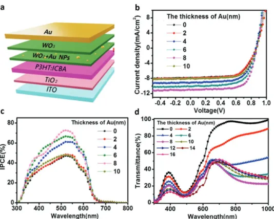
WO3, Au nanoparticles can automatically grow up through the process from nucleation in ultrathin coatings.[92] It was deter-mined that the photoconversion efficiency of P3HT based organic solar cell can be improved from 4.67% for bare sample to 6.63% for the optimal gold layer thickness of 8 nm.[92] The proposed design and its J–V characteristic have been plotted in Figure 10a,b. The incident photon conversion efficiency (IPCE) data have been extracted for bare and plasmonic samples. Figure 10c shows that the IPCE has been substantiated to a value as high as 80% at the incident light wavelength of ≈520 nm. The position of this peak is in accordance with the position of transmission dip in Figure 10d which means that a stronger light trapping is the origin of higher IPCE. As we can see from this panel, the transmission spectra do not signifi-cantly change after 12 nm Au thickness. This means that depo-sition of Au film leads to formation of nanoislands in sub-10 nm thicknesses and thicker layers form continuous film. Thinning down these trapping architectures is not only for boosting their photoconversion efficiency but it can also open up the opportu-nity to exploit them in flexible, wearable photoelectronics. An ink-printing CIGS based ultrathin flexible solar cell was pro-posed where the incorporation of nanoplasmonic units in the interface of pn junction have improved efficiency to a relatively high value of 10.36% (while the efficiency for bare structure was 8.31%).[93] This solar cell reveals near 80% flat EQE from 550 to 1100 nm. For a flexible bendable cell, the operation in angular incident lights is also of great importance. These scat-tering particles have omnidirectional response where the enhancement compared to bare structure becomes more Figure 10. a) The proposed plasmonically enhanced organic solar cell and b) its photocurrent–voltage response. c) The IPCE values for different Au
distinguishable at wider oblique angles. Besides these subwave-length colloidal nanoplasmonic particles, predesigned metallic nanoantennas can be made using lithography techniques to obtain a specific functionality. Tapered silver nanoantennas were used to couple the incident light into the active layer.[94] The effective trapping in these nano-objects stems from the excitation of collective modes of the plasmonic antenna strips and their coupling into semiconductor photonic modes. These nanostrips can be designated in a way that field localization within the metallic structure is much weaker than the gap between adjacent elements. Upon placing two nanoparticles at a deep subwavelength distance, their optically driven free elec-trons couple dynamically across the gap, and this causes a large field enhancements in the gap position. For a periodic pattern of nanoplasmonic units, this enhancement has a narrow spec-tral coverage[95] and this is not desired for photoconversion applications. However, in the random nanopatterns (such as colloidal assemblies or dewetted particles) with multiple gap distances, this light confinement can be achieved in a broad wavelength range.[96] Hence, in such designs, the incident power will be efficiently coupled into the semiconductor layer rather than being lost in metal. This coupling could be further intensified by the use of a reflective metal mirror. In this cavity design, the semiconductor active layer will be sandwiched by a planar mirror and trapping antenna where the formation of gap
plasmon resonance can substantially enhance light harvesting inside the semiconductor bulk. Gap plasmon resonance will be discussed in upcoming section. The proposed solar cell design, and its J–V response (in comparison with the bare cell) are rep-resented in Figure 11a,b. Moreover, Figure 11c,d depicts nor-malized electric field intensity distributions for the solar cell with ITO anode and cathode (λ = 840 nm) and with ITO anode and Al cathode (λ = 480 nm). As these panels clearly illustrate, for the case with ITO cathode, the strong light confinement is mainly achieved in the edges of nanoplasmonic antenna design. However, introduction of the bottom reflecting Al mirror as cathode provides strong field localization within the bulk of solar cell. This essentially stems from excitation of gap plas-monics in the cavity design. Another example of an innovative plasmonic design was to replace ITO layer with plasmonic cavity with subwavelength hole arrays.[97] Incorporation of this plasmonic unit enhances the EQE to a maximum value of 70% at around 600 nm while this value for the bare sample stays below 50% in the whole range. This partially transmissive/ reflective plasmonic architecture led to an improvement in device efficiency, η, from 2.9% to 4.4% which was among the highest achieved conversion values for P3HT/PCBM polymer solar cells.
As already stated, a part of light trapping improvement in the semiconductor-based devices is associated with light Figure 11. The a) proposed solar cell with nanoantenna design, and its c) J–V response compared to a bare cell. Normalized electric field intensity
distributions for the solar cell with c) ITO anode and cathode, λ = 840 nm d) and with ITO anode and Al cathode, λ = 480 nm. Reproduced with per-mission.[94] Copyright 2018, American Chemical Society.
scattering. The introduction of a reflective mirror and a spacer below the plasmonic structure (if designed properly) could maximize the optical path length of the scattered light.[94,98–103] This will, in principle, make a “10 nm limit” for efficient ultrathin solar cells possible.[98] A nanocavity based on Al-SiO
2 (55 nm) – Au nanoparticle was uniformly coated with 10 nm tin mono sulfide (SnS) where a broad and near unity absorp-tion was realized for such a thin coating.[101] It was found that this broad absorption behavior is attained via the superposition of two resonance modes; 1) due to the excitation of localized surface plasmons (LSPRs) and 2) first-order FP cavity modes. A wiser architecture is to replace the spacer with a conductive high bandgap metal oxide to enhance the probability of carrier separation. Butun et al. proposed a cavity structure made of an Al-NiOX-Ag-(monolayer MoS2) where the plasmonic antenna produces intense local fields and these confined modes are cou-pled to monolayer MoS2 to achieve 4 times higher absorption compared to that of a bare none cavity design.[102] The photo-luminescence measurements have demonstrated that most of the light absorption has occurred in MoS2 monolayer. More-over, injection of hot electrons from a plasmonic nanoantenna into a 2D semiconductor can be utilized for sub-bandgap photo-detection.[104] These metallic nanoantennas can be replaced with highly ceramics, such as titanium nitride (TiN).[105]
2.2.2. Plasmonic Nanostructured Mirrors
Another strategy to intensify the absorption capability of an ultrathin semiconductor layer is the utilization of nanostruc-tured back reflector. These metamirrors could be mainly obtained by nanoparticles or periodically patterned subwave-length units on optically thick reflector.[106–113] In the case of nanoparticle-based mirrors, the performance improvement is generally attributed to the scattering property of the plasmonic units. However, their contribution has been found to be weak, as explained in the previous section. The periodic pattern of nanostructures, such as gratings, patches, grooves, and holes, can significantly improve light absorption.[106–112] In one of the pioneer studies, a group of researchers in Atwater lab designed a nanogroove based reflector, tiled to be polarization inde-pendent.[114] They demonstrated that a single nanogroove under a 200 nm thick thin Si active layer can make above bandgap absorption 2.5 times stronger over 10 µm2 area. They found that this enhancement mainly originated from the coupling of the light into surface plasmon polaritons (SPPs) in a semicon-ductor-metal interface. Coupling to SPPs makes absorption confined in a mode volume which is dramatically smaller com-pared to the exponential decay profiles occurring in the bulk. It was shown that the right choice of grooves’ width and semicon-ductor layer thickness can maximize absorption in the active layer. It was envisioned that this strategy could be extended to other semiconductor types. A later study proposed a design based on Ag nanogratings filled by ITO and covered by a 100 nm thick Si layer.[115] According to the finite-difference time-domain (FDTD) simulation results, there are three mech-anisms responsible for light trapping enhancement in this nanostructured back mirror. The first mechanism was the for-mation of FP resonances in the metal–semiconductor double
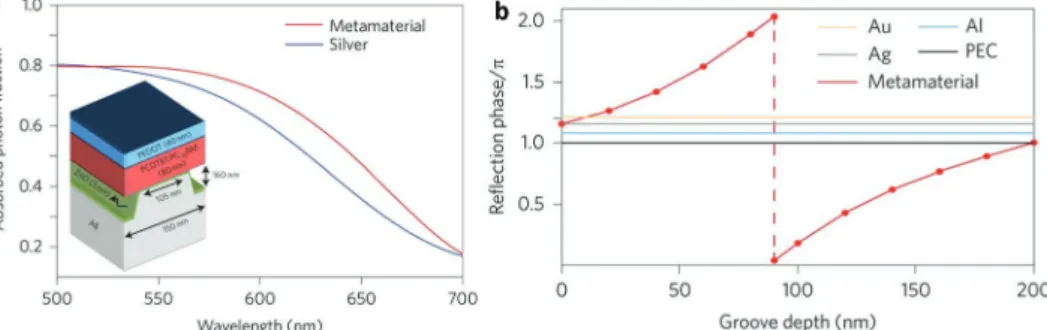
layer design. This resonance was red-shifted as we replace the plane metal with a nanograting design. This was due to the fact that the grating structure will effectively change the optical path length within the cavity. The width, height, and periodicity of the design can effectively tune the cavity optical length. While the plane MS structure has only FP resonance as the respon-sible mechanism for light harvesting, the grating structure can support SPPs in Ag-Si and Ag-ITO interfaces for TM polariza-tion. The third trapping scheme was attributed to the coupling of incident light into the a-Si planar waveguide. The excitation of guided mode resonances in a-Si slab waveguide leads to strong filed patterns within the active layer for both TE and TM polarizations. The superposition of these three resonance modes resulted in a broadband light trapping. Therefore, dif-ferent from previous discussed plasmonic nanoantennas, this nanostructure-based reflector can be used as a mean to tune and widen the spectral position of resonant absorption. One of the most frequently utilized metamirror designs is based on metallic nanogratings on a thick planar bottom mirror. This design was utilized to tailor absorption profile in a thin lossy film. It was theoretically shown that the decrease in the filling fraction of metal gratings (while the grating constant is fixed) will red-shift the FP resonance of the cavity.[116] In this state-ment, the filling fraction is grating width to grating constant ratio. In fact, as we make the grating narrower (while perio-dicity is kept constant), the design approaches to a planar MS junction with only the bottom metal as a reflector. This conse-quently causes the cavity length larger and resonance moves to longer wavelengths. This strategy is of particular interest in narrow bandgap semiconductors in which the absorption coef-ficient is much smaller in longer wavelengths (in comparison with that of short range). Thus, while the inherent high extinc-tion coefficient in UV and short visible range will provide light perfect absorption, the longer wavelengths will be harvested by the help of this metasurface back mirrors. Alongside with all of these effects, a metasurface mirror can be designed in a way that it acts as a magnetic mirror with near zero reflection phase. In a conventional bulk metal mirror, light takes π phase differ-ence as it hits the metal and thus a destructive phase differdiffer-ence (with a minimum field intensity) will be generated in the metal–semiconductor interface. Esfandyarpour et al. designed a groove shaped metamaterial mirror to tackle this problem.[117] The proposed design has been depicted in Figure 12a. As it can be deduced from this panel, the metamaterial-based design has higher absorption strength over a broad wavelength range. It was deduced that, while other metals have constant near π phase for a reflected wave, the groove depth in the metamate-rial mirror can be adjusted in a way that any arbitrary phase difference can be achieved. This has been shown in Figure 12b. Besides all these promising optical features, the realization of such a complex design is a challenging task. As depicted in Figure 12a, there is an air gap between the metamirror and the planar active layer. So, in the ideal case, the absorbing layer should be made as a thin coating on top of the grating without diffusing into the grooves. The authors have used spin-coating technique to deposit the active layer and no clear proof has been provided for the formation of a planar semiconductor layer. It has been noted by the authors that epitaxial lift-off and subsequent transfer process can be utilized to obtain the
proposed ideal design. As an alternative, the grooves can be filled with a transparent dielectric and chemical mechanical polishing (CMP) can be employed to planarize the structure before active layer coating. Apart from all the above-mentioned fabrication complexities, the main drawback with these type of designs is the polarization sensitivity of the grating structure where it can support SPP modes in TM polarization not in TE one. The replacement of this 1D elongated grating with peri-odic patches, or fishnet-like holes will reinforce the efficient operation of the structure in all light polarizations.[109,118,119] This is important for the practical application of this strategy considering the fact that the incident solar irradiation is also unpolarized. Besides these symmetric designs, the polarization insensitivity can be acquired by arrangement of gratings in a proper way.[120,121] A recent study proposed a metamaterial based mirror based on periodic patterns of Ag nanoparticles on Ag film.[122] Authors employed dark-field scattering spectroscopy
to scrutinize the mechanisms responsible for light absorption enhancement. LSPRs, propagating SPPs, and plasmon-absorp-tion-induced scattering were the main mechanisms responsible for light absorption enhancement in this metadesign. A later study demonstrated the applicability of this mirror in the absorption enhancement of MoS2−Organic van der Waals Het-erojunctions.[123] These metamirrors were utilized in flexible polymer solar cells.[124] Ou et al. demonstrated an efficient light trapping scheme based on simultaneous use of a silver mes-owire grid-based front transparent electrode (instead of ITO) and a plasmonic meta-mirror-based back reflector electrode (instead of a flat metal coating). As shown in Figure 13a, the groove is created on photoactive layer by imprinting quasi-random nanostructures on its surface. Atomic force micros-copy (AFM) shows the morphology of the mirror, see Figure 13b. As it can be calculated from J–V curves in Figure 13c, the use of metamirror has substantiated solar cell Figure 12. The proposed magnetic metamaterial mirror design. The reflection phase for different metals and metamaterial design at 600 nm light
irradiation as a function of groove depth. Reproduced with permission.[117] Copyright 2014, Springer Nature.
Figure 13. a) The proposed metamirror design, b) its AFM image, and c) J–V characteristic which shows improvement compared to a flat mirror-based
design. d) The proposed metamaterial-based design, and e) its light deflection profile. f) The photoresponsivity of the structure with and without metasurface mirror. a–c) Reproduced with permission.[124] Copyright 2016, Royal Society of Chemistry. d–f) Reproduced with permission.[125] Copyright 2018, American Chemical Society.