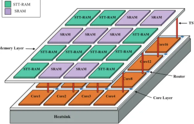
A heterogeneous memory organization with minimum energy consumption in 3D chip-multiprocessors
Tam metin
Şekil

Benzer Belgeler
This paper aimed to uncover how economic sanctions being external shocks affect the trends in fossil fuels and renewables share in total primary energy supply of targeted states
Similarly, for each 50 kW p decrement in the system size, the unit cost of the equipment rises with a rate of 8 €/kW p The parameters such as the annual PV
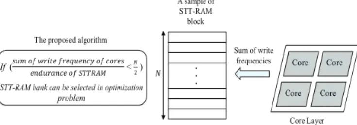
In this chapter, we propose a novel low power encoding approach to decrease the number of switching activities through decreasing the number of ones included
This thesis focuses on the routing issue in DTNs using limited resources and investigate the performance of four well-known DTN protocols which is Epidemic, PRoPHET,
Summary– Spontaneous coronary artery dissection (SCAD) is a rare and uncommon case of sudden cardiac death and acute coronary syndrome.. Herein, we present a 13-year-old boy
The volatility of these flows, the crisis in many countries (1992-93 ERM crisis, 1994-95 Tequila Crisis, 1997-98 East Asian financial crisis, 1998 Russian crisis, 1999
Tuluat sanatçısı ve sinema oyuncusu olduğu gibi, aynı zamanda tiyatro yöneticisi olarak da bütün ömrünü ve e- meğini, sahneye veren İsmail Dümbüllü, tam
Generating function approach introduces exact closed form expressions for the joint stationary queue length distribution and the conditional decomposition formula. Ex-
