» 4 І Г ' ■ ' T И fv V’ г ?
І|ч|(% т у
ІічІ
Г-М ^ · i f ¿ .¿ i ■ -C' ğJt-'T "^' ^ i^·*···^ ' ■' ? Д f \ * í Λ **“ í ^ff· Г;*Ѵ^ f>7 гГ' / ' » ?ATO M IC T H E O R Y
OF T H E
S C A N N IN G T U N N E L IN G
M IC R O SC O PE
A THESIS
SUBMITTED TO THE DEPARTMENT OF PHYSICS AND THE INSTITUTE OF GRADUATE STUDIES
OF BILKENT UNIVERSITY
IN PARTIAL FULFILLMENT OF THE REQUIREMENTS FOR THE DEGREE OF
MASTER OF SCIENCE
B y
A . E rk a n T E K M A N
..’
V с
} 2 п
I certify th a t I have read this thesis and th a t in my opinion it is fu lly adequate, in scope and quality as a dissertation for the degree o f M aster o f Science.
Prof. Dr. Salim Ciraci Principal Advisor
I certify that I have read this thesis and that in my opinion it is fully adequate, in scope and quality as a dissertation for the degree of Master of Science.
Prof. Dr. Cemal Yalabık
I certify that I have read this thesis and that in my opinion it is fully adequate, in scope and quality as a dissertation for the degree of Master of Science.
Assoc. Prof. Dr. Metin Durgut
I certify th a t I have read this thesis and th a t in my opinion it is fu lly adequate, in scope and quality as a dissertation for the degree o f M aster o f Science.
Assoc. Prof. Dr. Recai Ellialtioglu
I certify that I have read this thesis and that in my opinion it is fully adequate,
in scope and quality as a dissertation for the degree of Master of Science.
s . fe e c .·
Assoc. Prof. Dr. Şinasi Ellialtioğlu
Approved for the Institute of Graduate Studies
Director, Institute of Graduate Studies, Prof. Dr. Mehmet Baray
ABSTRACT
ATOMIC THEORY OF THE
SCANNING TUNNELING MICROSCOPE
TEKMAN, Ahmet Erkan
M. S. in Physics
Supervisor : Prof. Dr. Salim Çıracı
January 1988, 99 pages
The Scanning Tunneling Microscope is proven to be one of the most powerful tools for surface structure determination. Present theories are able to explain the operation of the microscope when the tip is far from the surface. For the small tip height case the atomic-scale interaction of the tip and the surface has to be included in the theory. The electronic structure of the combined system of the tip and the surface is calculated with an Empirical Tight Binding approach for graphite. It is found that in the vicinity of the tip some Tip Induced Localized States are formed. These states play an important role in the tunneling phenomenon. The contribution of these states to the tunneling current is calculated.
Key words: Scanning Tunneling Microscopy, Tunneling, Empirical Tight Binding, Tip Induced Localized States, Graphite.
ÖZETÇE
TARAMA TÜNELLEME
MİKROSKOBUNUN
ATOMSAL KURAMI
TEKMAN, Ahmet Erkan
Yüksek Lisans Tezi, Fizik Bölümü
Tez Yöneticisi : Prof. Dr. Salim Çıracı
Ocak 1988, 99 salıife
Tarama Tünelleme Mikroskobunun yüzey yapısı belirlenmesinde güçlü bir araç olduğu ortaya çıkmıştır. Şu ana kadar öne sürülen kuramlar uç yüzeyden uzakta iken mikroskobun çalışma ilkesini açıklayabilmektedirler. Ufak uç yüksekliği durumunda uç ile yüzey arasında atomik boyuttaki etkileşimin kurama eklenmesi gerekmektedir. Uç ve yüzeyin oluşturduğu bileşik sistemin elektronik yapısı Denemesel Sıkı Bağlanma yöntemi ile grafit için hesaplandı. Uç çevresinde Uç Güdümlenmiş Yöreselleşmiş Durumlar oluştuğu bulundu. Bu durumların tünellenme olayında önemli katkılarının olduğu gözlendi. Bu durumların tünelleme akımına katkıları hesaplandı.
Anahtar sözcükler: Tarama Tünelleme Mikroskobu, Tünelleme, Deneme sel sıkı Bağlanma, Uç Güdümlenmiş Yöreselleşmiş Durumlar, Grafit.
Acknowledgement
During the study on Scanning Tunneling Microscopy and preparation of this thesis my supervisor Prof. Dr. Salim (^iraci guided, helped and motivated me, with his constant decisiveness and his friendly, welcoming personality. Without his remarks, advices and ideas this study could not be completed.
I debt special thanks to Assoc. Prof. Dr. Metin Durgut, Assoc. Prof. Dr. Şinasi Ellialtioğlu and Assoc. Prof. Dr. Recai Ellialtioglu for their valuable remarks and discussions on the subject.
Finally I would like to thank to the Research Assistants of the Engineering and Science Faculty of Bilkent University for their continuous morale support, especially to Oğuz Giilseren for his accompaniments while this study was on progress, and to Ilhami Torunoglu for his guiding comments on my dissertation talk.
Table o f C ontents
A b s t r a c t ... Ö z e t ç e ... jjj A ck n o w led g em en t... iv Table of C o n t e n t s ... v List of F i g u r e s ...vii List of T a b le s ... .. ^ 1 In tro d u ctio n 12 A Survey of Scanning Tunneling Microscopy
2.1 Experimental Technique of Scanning Tunneling Microscopy
2.2 Experimental Results of Scanning Tunneling Microscopy... 11
2.3 Theories for Scanning Tunneling Microscopy... 16
3.1 An Atomic Approach to Scanning Tunneling Microscopy of
Graphite 28
3.1.1 Electronic Structure of Graphite and the T i p ... 28 3.1.2 Theories for Scanning Tunneling Mici’oscopy of Graphite . 36
3.2 Energy Band Calculations and Tip Induced Localized States 44
3.2.1 Method of Calculations 44
3.2.2 Results of Calculations... 53
4 T unneling C urrent for Sm all T ip H eight R egim e 68
4.1 Bardeen’s Formalism for Tunneling... 68
4.2 Tunneling Current in the Presence of Tip Induced Localized States 73 4.3 A Simple Model for the Effects of Tip-Surface Interaction . . . . 76 4.4 Tunneling Current For Small Tip Heights: G ra p h ite ... 81
5 C onclusions and D iscu ssion 89
List o f Figures
2.1 A schematic description of the scanning tunneling microscope . . 6
2.2 A pocket-size scanning tunneling microscope 9 2.3 Relief of Si (111) surface-reconstructed (7 x 7) 13 2.4 Scanning tunneling microscope image of g ra p h ite ... 15
2.5 Anomalous corrugation amplitudes for g ra p h ite... 16
3.1 Structure of g rap h ite... .. ... 29
3.2 Brillouin zone of g r a p h ite ... 31
3.3 Field-ion pattern of mono-atomic t i p ... 35
3.4 Local density of states for graphite s l a b ... 38
3.5 Corrugation amplitude as a function of tunneling current 41 3.6 Electronic energy band structure of graphite monolayer 50 3.7 Band structure for the on-top p osition-I... 56
3.8 Band structure for the on-top position-II... 60
3.9 Local density of states for TSi ... 62
3.10 Band structure for the hollow-site position... 64
3.11 Band structure for the bridge p o sitio n ... 66
4.2 Local density of states in the vertical plane for graphite monolayer 83 4.3 Energies of tip induced localized s ta te s ... 84 4.4 Energies of tip induced localized states: On-Top Position 85 4.5 Tunneling current... 86 4.6 Tunneling current along special directions... 87
List o f Tables
3.1 Fitted Hamiltonian matrix elements (eV) 49
3.2 The model wavefunctions and scaling... 51 3.3 The band results for the on-top p o sitio n ... 63 3.4 The band results for the bridge p o sitio n ... 67
C hapter 1
In trod u ction
It has been known since the first years of the quantum mechanics that, particles can be found in the regions of space, which classical mechanics excludes, with a nonzero probability. This statement is a result of the wave-particle duality, and henceforth Heisenberg uncertainity principle. The tunneling phenomenon is a special demonstration of this fact. In tunneling, a particle transferred between two classically allowed regions by passing through a classically forbidden barrier region. Tunneling phenomena in solids have been investigated for a large number of different systems and is shown to be one of the basic physical events.
The first application of tunneling was done by Oppenheimer [1] in 1928 to analyze the effects of huge electric fields on hydrogen atoms. He predicted an auto-ionization as a result of the formation of a lowered potential barrier in the direction of electric field. His study on the field emission was the basis of the subsequent theories of tunneling. In 1928 Fowler and Nordheim [2] explained the field emission from metals, which was observed in 1922, but was unexplained
since then, using the quantum mechanical theory of tunneling. There were other applications of tunneling in nuclear and atomic physics, which were treated in late-twenties [3]. In 1930 Frenkel [4] proposed a tunneling approach to the metal-metal junction resistances, which became the basis of the later solid state tunneling experiments. Nevertheless, the solid state physics is not the only area of physics in which, tunneling plays an important role.
After mid-fifties parallel to the development of the electronic devices, tunneling experiments in solid state systems attracted interest. In 1958 the p-n tunnel diode was proposed by Esaki [5]. For this invention he was awarded the Nobel Prize in Physics in 1960. In sixties tunneling experiments were held with superconducting structures and the coupling of superconducting systems could be understood in terms of tunneling.
One of the most striking applications of tunneling was realized in early- eighties for analyzing the surface structure of solids with an atomic-scale resolution . The first Scanning Tunneling Microscope was built by G. Binnig and H. Rohrer [6,7] in 1982. Since then the microscope has been developed into a widely used precise imaging tool. After this invention Binnig and Rohrer were awarded the Nobel Prize in Physics in 1986.
The underlying physical idea for the Scanning Tunneling Microscope is just the theory of tunneling. Previous applications of tunneling in solids were
made with solid insulating barriers [3]. Therefore the electrode-barrier-electrode structure was not variable for these cases. However, if one can change the geometry of the structure the tunneling phenomenon will also differ. This change in tunneling process is related to both the change of the structure and the quantum mechanical properties of the electrodes and the barrier. When one uses a vacuum barrier, and if the quantum mechanical state of one of the electrodes is known, then one can get information about the other electrode by analyzing the change in tunneling data [8].
The Scanning Tunneling Microscope essentially consists of a metal tip, the position of which can be controlled very accurately, a vacuum barrier which can be controlled by the position of the tip, and the sample surface to be investigated. While measuring the current at different lateral positions one can attain the surface topography with atomic resolution [6,7,9].
The set-up of the Scanning Tunneling Microscope has been developed since it was first proposed [10]. Nowadays it is possible to put the mechanical part of a microscope, which has atomic resolution, into a pocket-sized apparatus. Nevertheless there are still some unexplained problems. These are mainly anomalous corrugations which are not consistent with the electronic structure or the symmetry of the surface.
Bardeen’s formalism [11] for tunneling. In this method the electrodes are assumed to be independent of each other. However, for small tip-surface separations, the atomic scale interactions between the tip and the surface have to be included in the theory.
In this thesis I will analyze the atomic scale effects of the tip-surface interaction on tunneling. In Chapter 2 a survey of the experimental and theoretical studies on Scanning Tunneling Microscopy will be given. In Chapter 3 special emphasis will be given to one of the important cases in Scanning Tunneling Microscopy, namely graphite surface, and the effect of the tip structure. In this chapter methods of calculations, and the results for electronic structure of the tip-surface combined system will be given. The effects of these results on the tunneling will be investigated in Chapter 4. General discussions and concluding remarks will be presented in Chapter 5.
C hapter 2
A Survey o f Scanning T unneling
M icroscopy
2.1
E x p erim en ta l T echnique o f S can n in g Tun
n elin g M icroscop y
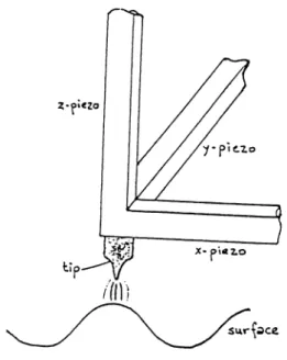
Originating from the idea of using a metal tip as one of the electrodes, a controllable vacuum gap as the insulating barrier, and a sample surface as the second electrode, Binnig and Rohrer [6,7,8,9] built up a basic tool for investigating the solid surfaces. The so-called Scanning Tunneling Microscope consisted of a metal tip, a piezoelectric translator for varying the position of the tip and a sample surface to be detected. The schematic setup of a Scanning Tunneling Microscope is shown in Figure 2.1.
Applying a bias to the tip with respect to the surface and carrying the tip to the close proximity of the surface with a small vacuum gap in between, there will be a tunneling current between the tip and the surface. One can change the
Figure 2.1: A schematic description of the scanning; tunneling; microscope position of the tip with respect to the surface by using the translators, and thus obtain the tunneling current as a function of position. It is clear that this change in the tunneling current is closely related to the quantum mechanical state of the surface. Therefore these scans are characteristic images of the surfaces.
Having obtained the characteristic scans, the second step for surface structure determination is to relate them to the topographical, electronic and other properties of the surfaces. The first interpretation of Scanning Tunneling Microscopy was proposed by the inventors themselves [6,7]. It is clear from the previous theoretical work on tunneling that the tunneling current from the tip to the surface is caused by the overlapping exponential-like tails of wavefunctions of the tip and the surface. Hence by changing the position of the tip, the overlap of these tails will change, so will the tunneling current. Since the tip
wavefunction is assumed to be unaltered, the tunneling current will be related to the wavefunction of the substrate in the vicinity of the tip.
At this point one can mention the basic advantage of the Scanning Tunneling Microscope. Since the tunneling current is related to the wavefunction of the surface at the vicinity of the tip, Scanning Tunneling Microscope can make in situ real space measurements. There is need for neither a periodicity, as in the X-ray diffraction or Low Energy Electron Diffraction, nor a large density of states in a microscopically large area, as in the Electron Energy Loss Spectroscopy or Scanning Electron Microscopy [12]. Even small clusters like biological molecules [13] or single defects on surfaces such as adsorbates [14] or steps [7] can be observed with a good resolution.
Initially it was conjectured that when the tip is at the on-top position of one of the surface atoms, the surface wavefunction will have a large magnitude and the current will be large. Away from the on-top position the overlap of the wavefunctions and hence the current will decrease. Therefore, according to this interpretation the line scans of Scanning Tunneling Microscopy will directly reproduce the surface topography [7].
Based on the above theory the basic operation mode of the Scanning Tunneling Microscope was arranged as follows. A fixed voltage bias is applied between the tip and the surface. The height of the tip arranged to yield
a constant tunneling current while the tip scans the surface. This mode of operation is called the constant voltage-constant current mode [7,12] of the Scanning Tunneling Microscope. Since the tunneling current is related to the surface wavefunction, the height of the tip will be a measure of the magnitude of the wavefunction. Hence the density profile of the surface can be extracted from the scanning data.
The first Scanning Tunneling Microscope was a large apparatus [9] since some very precise supporting tools were used for isolating the system from vibrations and obtaining an ultra high vacuum. This so-called first generation Scanning Tunneling Microscope has been developed with some new considerations. Furthermore, some observations showed that the environmental disturbances may be so small that the use of simple isolating equipment would be sufEcient[7,12j. Hence, nowadays for most of the applications the so-called
Pocket-Size Scanning Tunneling Microscope [10,12] is commonly used. In
addition ultra high vacuum and low temperatures are not necessary for a large variety of experiments. Therefore, experiments can be done in air [14], or even in some liquids [15,16,17] and at room temperature. These developments made the Scanning Tunneling Microscope a practical and feasible tool for surface studies. As a result, today over 200 laboratories are using Scanning Tunneling Microscopes in their studies.
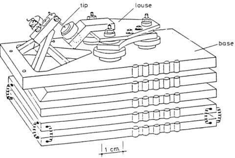
Figure 2.2: A pocket-size scanning tunneling microscope
The scale shown at the bottom corresponds to 1 cm. The drawing is taken from Reference [12]. @1986, American Institute of Physics.
Microscope is shown. The basic parts of the microscope are as follows [12];
1. The sample holder is attached to a stepper (louse) consisting of a tripod attached to a piezoelectric body. The louse stands on a steel plate using three anodized aluminum pods. These pods are not solidly connected to the plate, but the louse is electrostatically clamped to the plate. By setting one of the pods free and applying a voltage across the piezoelectric body to change its length one can move the feet on the plate. This procedure is applied several times to get the sample to the proximity of the tip with a coarse adjustment. The sample holder is made of a light metal such as titanium, and a few clamps are used to fix the sample on the holder.
2. The base of the microscope is made of a number of steel plates, separated by viton pieces for absorbing the external vibrations. This system is not effective at low temperatures and it is necessary to use more complicated vibration isolation equipments.
.3. The tip holder is also made of a light metal. It is connected to a piezoelectrical tripod (scanner). Usually there are electronic units to control the X - , y- and z-scan of the tip. By applying voltages to the
feet of the tripod, controllable displacements of the order of 0.1 A can be achieved.
4. The louse, the sample holder, the scanner and the tip holder are connected to the external circuitry. Most of the operation is controlled, and the results are analyzed by a computer.
The basic operation principle of the microscope can be summarized as [12]:
1. The sample is clamped to the holder and by using the stepper, the louse is brought to the close proximity of the tip, that is to a distance of the order of 0.01 mm.
2. A constant voltage bias is applied across the tip-surface barrier. The surface is scanned while adjusting the position of the tip by using the piezo tripod keeping the tunneling current held constant, the surface is scanned. The typical scanning speed is 100 A/sec . Typical resolution of the tip position is 1 A for x- and y-scans, and 0.1 A for z-scan.
•3. The resulting line scans are analyzed to obtain a grey-scale image of the surface by a computer. This is the final data of a Scanning Tunneling Microscopy experiment and includes all the information which can be collected in the constant voltage-constant current mode. The variation of tip height as a function of lateral position is called corrugation and the maximum value of corrugation is called corrugation amplitude.
2.2
E x p erim en ta l R esu lts o f S can n in g T u n n el
in g M icroscop y
In Section 2.1 the basic principles of the Scanning Tunneling Microscope were introduced. In this section special emphasis will be given to the experimental results which were obtained by using Scanning Tunneling Microscopy. As it was mentioned, the local character of the imaging is one of the main advantages of this microscope. Therefore it is very appropriate to use it for structure determination experiments on some complicated surfaces and molecules.
Nevertheless, the Scanning Tunneling Microscope was first used on metal surfaces [18,19]. Since the tunneling phenomenon depends on the flow of a current, it is important for the sample to have a conducting character. Because of its atomic scale resolution, the microscope is a very good candidate for determining the reconstruction of metal surfaces.
In 1983 and 1984 the inventors used Scanning Tunneling Microscopy to find the reconstruction schemes of Au (110) [18] and (100) [19] surfaces. For (110) they observed (1 x 2) and (1 x 3) reconstructed geometries, which have sawtooth like profiles consisted of energetically favorable (111) triangular facets. On the other hand, for the (100) surface several (1x5) reconstruction geometries are observed. These are the first results of Scanning Tunneling Microscopy with atomic scale resolution.
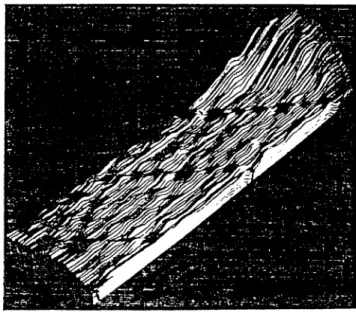
One of the most striking applications of Scanning Tunneling Microscopy is on the Si (111) surface, reconstructed in a (7 x 7) geometry [20]. This reconstruction scheme is hard to analyze as a result of the large unit cell, containing 49 atoms of the surface. The Scanning Tunneling Microscopy results were very accurate and consistent with the known parameters, such as the size of the 7 x 7 unit cell. The relief of the surface which includes two complete unit cells is shown in Figure 2.3. This pictoresque result was obtained by the inventors. In each unit cell twelve maxima and nine deep minima are observed. The minima pattern shows threefold rotational symmetry, whereas the maxima exhibit sixfold rotational symmetry around the rhombohedron corners. This result is in agreement with the “milk-stool” model of Snyder et al. [21] or the modified adatom model of Harrison [22]. As seen the imaging method has an atomic scale resolution to give a clearcut picture of the reconstruction scheme, and to guide the further research.
Figure 2.3: Relief of Si (HI) surface-reconstructed (7 x 7)
Two complete unit cells are clearly visible with atomic scale resolution. The figure is taken from Reference [20]. © 1983, The American Physical Society.
Scanning Tunneling Microscopy is used on grating surfaces, steps and single atom defects as well [10]. The results are at least as precise as those obtained by any other surface structure determination method. Observation of single atom steps, single atom defects and adatoms with atomic scale resolution are signs for the strength of the method [7]. Even some complicated biological molecules are investigated by using a flat surface metal as a background [13]. All of these results can not be achieved by a single surface imaging tool, other than Scanning Tunneling Microscope.
The preceding examples give an idea about the power of Scanning Tunnel ing Microscopy for surface structure determination experiments. Nevertheless
there are some special cases for which the results of Scanning Tunneling Microscopy are not acceptable as far as the surface topography is concerned. The most striking example for these anomalous results is the graphite surface.
Graphite surface is one of the most easily investigated structures by using the Scanning Tunneling Microscope [10,12,14,17,23,24,25]. The surface is extremely inert as compared to the other substrates studied so far. Inertness of the surface and the distinct electronic properties lead to the atomic scale imaging under extremely varying environments. Atomic resolution is attainable in vacuum, in air [14] and when immersed in a liquid [17]. In addition to that it is very easy to prepare precisely oriented graphite surfaces, flat over microscopically large regions.
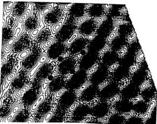
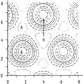
A typical Scanning Tunneling Microscopy image of the graphite surface is shown in Figure 2.4 [26]. The image was taken at a tunneling voltage of 50 mV. The corrugation amplitude is about 1.3 A. Owing to the symmetry properties of the graphite, which will be explained in Section 3.1.2, the honeycomb structure is not apparent in the image. Instead, two different kinds of carbon sites are found. The graphite surface is one of the structures that give most satisfactory results, excluding the small current experiments. Similar images were obtained by several groups with consistent corrugations.
Figure 2.4: Scanning tunneling microscope image of graphite
The dark regions are corresponding to smaller current. Full lines build up the unit cell and the dashed lines show the hexagon. Full (open) circles are B-type (A-type) atoms. The asymmetry between the two basis atoms is clearly visible. The figure is
taken from Reference [26]
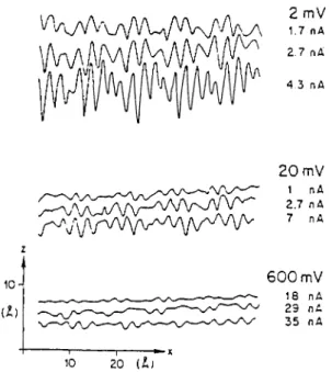
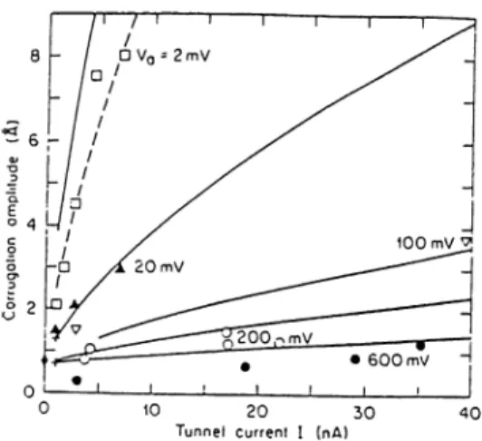
increase in the corrugation amplitude was observed. One of these experimental results is shown in Figure 2.5 [23]. Several authors reported corrugations up to order of 10 A [10,14,17]. It is clear that for small tunneling voltages the tip-surface separation will become smaller. Hence this giant corrugations are explainable only if this small separation regime is analyzed. In addition, there is a possibility of contamination of the tip for small tip heights. Several experimentalists reported that, it is not rare to hit the surface with the tip and take some surface atoms on the tip [14,27,28]. This situation is also common in microscopy of semiconductor surfaces. Thus, it is very difficult to have clear scans of these surfaces and to differentiate between the anomalous results.
charge-'/V \y V V '" V y ^ V Y ^ A ^ v /'·^ ^ 1 7 n A 2.7 nA 4 3 nA 20 mV 1 n A , 2.7 nA y - . Y ^ y ' V V \ / V ' A / ) ^ / \ / ^ A / \ y ^ 7 10-1 (¿) 600 mV 18 nA 23 nA 35 nA 10 20 i l l
Figure 2.5: Anomalous corrugation amplitudes for graphite
The tip height is shown for one scan. The corresponding bias voltage and tunneling current are indicated. The figure is taken from Reference [23]
density wave systems [29]. For lH-TaSe2 some large corrugation amplitudes were reported. This is not the case for 2H-TaSe2 structure. The explanation of these anomalous results are nearly the same as those of graphite, which will be described in detail in Section 3.1.2.
2.3
T h eories for Scan n in g T u n n elin g M icroscop y
As mentioned in Section 2.1 the interpretation of the Scanning Tunneling Microscopy data in terms of surface properties is one of the main objectives. The initial explanation of microscopy, assumes that the corrugation is a measure of the surface wavefunction, and thus the surface charge density. For the metallic
surfaces there is cilmost no need for further analysis since the Fermi surfaces of these materials are extended, and the local density of states is not very different from the total charge density. Hence the line scans are topographical images of the charge density, as pointed out by the inventors [6,7].
Later on Scanning Tunneling Microscopy was used on metallic surfaces with small Fermi surfaces, and even on semiconducting or insulating surfaces. For these materials the preceding explanation is no more valid, and there is a need for a general theory for Scanning Tunneling Microscopy. In order to examine tunneling from the tip to the surface in detail several models were proposed. In this Section I will give a brief summary of these theories.
One of the first ideas was directly solving the Schrödinger equation in the presence of a corrugated surface and thus calculating the tunneling current [30]. One-dimensional version of this problem is a classical subject in quantum mechanics textbooks. Garcia et al. [30] used a highly corrugated constant potential region for modeling the tip and a smoothly corrugated constant potential region for modeling the surface. Both of the structures were taken to be periodic; the surface with a period of lateral lattice constant and the tip with a period large enough to decouple the neighboring tips. In addition, they did not use the realistic barrier potential, which includes the effects of work-function difference of the tip and the surface, image field effects and self-consistent field corrections. Instead, they used a rectangular potential barrier of height </?, which
can be thought as the average work-function of the electrodes. The solutions were expanded in terms of plane waves and the resulting matrix equation was solved. They calculated the local current distribution in the barrier and found the tunneling current expression as:
eU
I = ^ G N{Ep) exp [-2.14 d|
2m (2.1)
In this equation N{Ep) is the density of states at Fermi level for the tip, Vq
is the bias applied, and d is the tip to surface distance. G is a geometrical constant, without any dependence on the other parameters.
This result is similar to those of plane surfaces, but due to the curvature of the surface there is a factor 2.14 in the exponent instead of 2 for a plane. Garcia et al. also investigated the effects of barrier height ip and effective curvature Ref/, defined as the geometric average of the curvatures of the tip and the surface, on the observed corrugation amplitude. They concluded that in order to obtain the real corrugation of the surface the tip have to be very sharp. They analyzed the experimental results for Au (110)(1 x 2) reconstructed surface. They have calculated the effective tip radius as ~ 3.5 A and the maximum tip height as ~ 3.9 A. Their results showed that the output of Scanning Tunneling Microscopy is far from being a direct image of the surface topography, and have to be analyzed carefully to obtain the physically acceptable results.
A more extended study based on similar approximations was proposed by Stoll et al. in 1983 [31]. They used the same structure as Garcia et al. [30] but
put emphasis on the boundary value matching, instead of solving the problem as a whole. They obtained the transmission coefficient as a function of lateral wave-vector. The sum of these contributions of all the wave-vectors yielded the total tunneling current. Using an expansion around the zero lateral wave-vector and a local approximation to the transmissivity they calculated the tunneling current as:
8 7Г
--iS exp [ - 2 ( ^ ) · / ^ dl ( R , n l d f l ^ (2.2) Here ^iicl Uefj are the geometrical averages of the two Fermi levels and heights of potential wells, respectively. E is the incident current, and .Re// is defined as the inverse of the arithmetic average of inverse curvatures.
Stoll et al. also obtained the local current density and tip scan curves for the constant voltage-constant current mode. They analyzed the effective radius of the tip by using the local current density. Their total current expression implies that the exponential dependence of the current on the tip height has a factor 2. Nevertheless, this approximation neglects the effects of the higher Fourier components of the incident current. Their simple fitting results in a factor of 2.08. However, they pointed out that in three dimensions this factor would be increased, and it will be close to the value found by Garcia et al. [30] . They have found that the resolution of the microscope decreases with increasing tip size and increasing tip height.
solving the Schrödinger equation using ~ 20 plane waves one can get the local current distribution, and the tunneling current can be calculated easily. Nevertheless, it has some drawbacks which limit its applicability to more complicated systems. The starting point of the theory is a free-electron approximation, which assumes that the potentials are flat in the tip,surface and barrier regions and the transitions are abrupt. This approximation is reasonable for metallic electrodes. However, for semiconductors or metals with small Fermi surfaces, free-electron-like solutions are far from being realistic. In addition the use of an extended tip body with periodic large corrugations for modeling the tip may cause some artifacts. Tunneling from the tip body to the surface has to be excluded from the total tunneling current, otherwise there will be a background conductance which can lead to erroneous results. The effects of periodic tip may also cause some problems. This multi-tip model has some extra contributions to the tunneling current due to the artificial periodicity of the tip.
More recent theories originate from the quantum mechanical theory of tunneling instead of the basic quantum mechanics methods like plane-wave-like solutions. The simplest theory which can be applied to Scanning Tunneling Microscopy was proposed by Bardeen in 1961 [11]. He treated the tunneling as a transition between the many-body states of two uncoupled systems, which are interacting through a transfer Hamiltonian. Applying the first-order time- dependent perturbation theory one can find the tunneling current as:
/ = 27T e
where ¡j. and u label the tip and the surface wave-functions, respectively. Here / is the Fermi-Dirac distribution factor and takes care of the statistical probability of a particular tunneling event to happen, V is the applied bias and Mfj,^ is the transition matrix element between the tip state /i and the surface statue u. Bardeen showed that this matrix element can be written as:
=
2 m (2.4)
The integral is to be taken over any surface lying completely inside the barrier region. It is clear that the expression in the parantheses is the current operator for a general quantum mechanical system. However, one has to bear in mind the special feature of this system which is explained below.
The difference of Equation 2.3 with respect to the ordinary time- dependent perturbation theory is on the overcompleteness of the basis set. The states and 7/>^ are solutions of the isolated tip and surface Hamiltonians, respectively. Therefore, each set is complete and we can express the solution in terms of either one of them. However, since the tunneling is a transition between two systems separated from each other by a classically forbidden region, we can see that it is approximately equal to an element of one set at i —>· — oo and to an element of the other set at i —»■ oo. Thus, it is more appropriate to expand the tunneling solution 'F in terms of both sets. This point will be discussed in detail in Chapter 4.
several authors for explaining Scanning Tunneling Microscopy. The most frequently referred theory for the Scanning Tunneling Microscope was proposed by Tersoif and Hamann in 1983 [32,33]. They took Bardeen’s tunneling current expression as the starting point of their work. They used the following model wavefunction for the surface;
■0^ = exp[(«^+ I KG d] exp(i kq ■ p) (2.5)
a
where Qs is the normalization volume, k — h~^{2rrupyl'^, and kq = ¿y + G is the
extended scheme surface state Bloch wave-vector, p is the lateral component of the position vector, and the summation is over the reciprocal lattice vectors of the surface. They modeled the tip as a locally spherical potential well. Taking the local curvature of the tip as the radius of the sphere and using the asymptotic spherical form of the wavefunction they found:
Cl K .R I c - ro I)·'
(
2.
6)
where is the normalization volume, ct a geometrical normalization constant of the order of one, and tq is the position of the center of the sphere. Note thatthe work-functions of the tip and the surface are assumed to be the same and only the s-type wavefunction of the tip is used.
Inserting these wavefunctions into Equation 2.3 and assuming that the bias is negligibly small compared to other energy measures, they found for tunneling current to be:
I = ^2TT^n-^e'^Vip'^Nt{EF)B}K-^t^'^^ ^ | V’v(ro) P S{E, - Ep) (2.7)
where Nt(Ep) is the density of tip states at the Fermi level. In a more tractable form the tunneling conductance can be written as:
<7 <x piro^Ep) (2.8)
where p{fQ,Ep) is the local density of states at the Fermi level and evaluated at the position of the tip.
Tersoff and Hamann commented that the appearance of the value of surface wavefunction at the position of the center of the tip is not a physical expectation but resulted from analytic properties of the model wavefunctions used [33]. For large tip heights they also arrived to behavior for the tunneling current. They applied their theory to Au(llO) scans for two different reconstruction schemes and had a c|uite good agreement with the experimental results. They also reported that Scanning Tunneling Microscopy is not sensitive to structural deviations for particular reconstructions at low voltage, that is large height regime.
Recently Chung et al. [34] included the effects of higher angular momentum states of the spherical tip in the tunneling current expression. They have found that for the case of accidental degeneracy of s- and d-states an additional current contribution from the d-state would arise and would be approximately 10% of the s-state current. They also calculated the resolution of the microscope and found that the results of completely different approaches yield similar forms.
This theory has a drawback about the shape of the tip. Using a sphere instead of an almost arbitrarily shaped tip with a curvature restricts the applicability of the theory. In addition, a disconnected sphere representing the tip would not have any electrical connection for a current passing through. Therefore application of Bardeen’s procedure to this geometry is not totally correct, since the tip describes a quasi-stationary state instead of a sink. Recently Chen [35] used a parabolic tip for overriding this difficulty and found a tunneling current expression in terms of Kummer’s functions.
Feuchtwang et al. [36] showed that the tunneling current can be found as a convolution of the tip and the surface spectral density functions. They emphasised the effects of the microscopic structure of the tip. They arrived at the conclusion that the incidence angle would be a determining factor for the effective barrier height seen by the electrons. An advantage of this method is its applicability for all types of tip structure. These results converge to those of Tersoff and Hamann in that limit. However, calculation of the spectral density functions is a tedious task and this procedure is not practical except for some special cases and requires information about the microscopic structure of the tip.
In 1984 Baratoff [37] made a review of the proposed theories and discussed some crucial points of Scanning Tunneling Microscopy. He pointed out that the electronic structure of the surface determines the completeness of the result of
Scanning Tunneling Spectroscopy and showed that it could be necessary to make different type of scans to get a thorough topographical image of the surface, for example to image both filled and empty bands of the semiconductor surfaces.
Baratoff also commented on the independent electrode approximation that was used by all earlier theories [37]. Actually, this is one of the most important deficiency of the theories reviewed above. This approximation can be assumed to hold for large tip heights. On the other hand, for small height cases there is a nonnegligible interaction between the tip and the surface, so that the wave- functions used in Equation 2.3 are no more acceptable solutions.
Very recently Feuchtwang and Cutler [38] gave a survey of the studies on Scanning Tunneling Microscopy and criticized the existing theories. They also pointed out the general problems arising from the tunneling theory itself. They drew attention to the probable resonance mechanisms in Scanning Tunneling Microscopy. These mechanisms are mainly related to the image field effects such as bound states and potential resonances.
Some theories concerning the atomic aspects of the tunneling and Scanning Tunneling Microscopy were also developed. Lang [39,40,41] proposed a system for analyzing the local effects of the atoms in 1985. He used electrodes consisting of a semi-infinite jelium and an adsorbate atom. He solved the independent electrode Hamiltonians to find the states which are participating in tunneling.
Using these wavefunctions he foiind the total time dependent wavefunction for the coupled two-electrode system. The current density is straightforward from bcisic quantum mechanics:
] = V ^ ImCf. V i(B„ - Ef) (2.9)
which reduces to:
j~ =f V Z «(-E, - Ejr) 6(E, - Ef) (2.10)
where and are the local and total current operator expectation values between the tip states labeled by /.i and the surface states labeled by 1/, respectively. This expression is equivalent to Bardeen’s formula for the tunneling current.
Lang also analyzed the effects of symmetric and energetic effects of the adsorbate atoms on the tunneling current. However, he has chosen the atom species according to their ease of computation, and therefore, his conclusions are not directly applicable to Scanning Tunneling Microscopy.
Recently Doyen and Drakova [42] used a method of chemisorption theory for describing the effect of the tip-surface interaction. They took the effects of this interaction into account by modifying the tip states. Their current expression is:
1 = 2 7T e
where ¡j. and ¡.l' label a convenient set of orbitals localized at the vicinity of
the tip and represent the outermost tip atom. S is square root of the sum of squared projections of the surface and the extended tip states on these localized orbitals. A’s can be approximated by Kronecker deltas. iy(/j) is the normalized potential element between the tip atom and the surface. They used this method for finding the scans for a step on a flat W (110) surface but as a result of the large tip height they used, they did not find any additional effect due to the tip-surface interaction.
As discussed in this section, the theory of the Scanning Tunneling Microscope is far from being complete. Every method has its own drawbacks, and as a result of the complexity of some experimental results, theories can not rigorously tested. It is clear that methods from other areas of physics will be beneficial for arriving at a conclusive theory.
A number of theoretical and experimental studies indicates the atomic nature of tunneling between the tip and the surface. Although the real tip is a very large and nonuniform cluster of atoms, the resulting corrugation images seem to be related to the outermost atom. For small tip heights one expects to have atomic scale interactions between the surface and tip atoms. The correct description lies somewhere between independent tunneling and chemisorption theory.
Chapter 3
A nalysis of th e Tip Induced
Localized States
3.1
A n A tom ic A pproach to Scanning T unnel
ing M icroscop y o f G raph ite
3.1.1 E lectron ic S tru ctu re o f G rap h ite and th e T ip
As commented in Chapter 2 one has to use an atomic method to consider the interaction of the tip and the surface at small tip heights in order to analyze the reasons of anomalous results of Scanning Tunneling Microscopy. Graphite is a very appropriate candidate for this purpose, since its semi-metallic character makes it necessary to put the tip in very close proximity of the surface for obtaining reasonable tunneling currents. Therefore, graphite will be the subject matter of the rest of this work. Arguments similar to those that will be made for graphite can also be applied to other structures, such as semiconductors and other semi-metals.
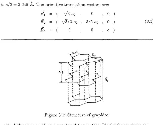
Graphite has a very anisotropic crystal structure [43]. It basically consists of honeycomb-like layers, which are in turn loosely bound to the adjacent layers. The crystal structure is shown in Figure 3.1. In a layer there are two different types of carbon atom sites as far as their bonding arrangements are concerned. Half of them have carbon atoms in the neighboring layers which are directly above or below them; these are designated as A-type atoms. The other half have centers of hexagons directly above or below them; designated as B-type atoms. The nearest-neighbor distance is Qq = 1.418 A and the interlayer spacing is c/2 = 3.348 A. The primitive translation vectors are:
Ri = ( Go , 0 , 0 )
R2 = ( V3 / 2 ao , 3/2 ao , 0 ) (3.1)
R3 = ( 0 , 0 . C )
Figure 3.1: Structure of graphite
The dark arrows are the principal translation vectors. The full (open) circles are A-type (B-type) atoms.
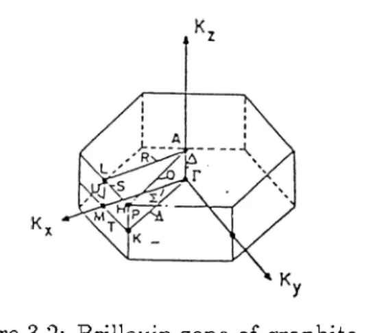
group is isomorphic to Df^h- There are two inversion centers, one is halfway between the two adjacent A-type atoms, and the other is obtained from the first one by translating it in the parallel the layers by half a primitive translation vector. The local symmetry about the atoms is the same for A- and B-type atoms and is isomorphic to the group Dzh- The Brillouin zone of the reciprocal lattice is shown in Figure 3.2. The center of the Brillouin zone is the F point and the point group is D^h- This group has a two-dimensional representation
E' according to which (x, y) transforms. This leads to degeneracy of the px and Py originated bands at the F point. On the line connecting F to H, the point
group is Czv and it has a two-dimensional representation, compatible with E'. At the H point on the top surface of the Brillouin zone the group is again Dzh- At the corner of the = 0 cross-section of the zone, namely at K point, the
point group is Czh- This group has a two-dimensional representation for (x, y). Along the line connecting K to the top surface, the point group is Cz- At the top surface, P point, the point group is again Czv Along this line the two- dimensional representation is continuous.
Carbon is a tetravalent atom having a closed shell Is orbital and a half- filled 2s 2p^ shell. The electronic structure of the graphite can be understood in terms of crystal structure and the electronic structure of the carbon atom. Since the interlayer spacing, c, is much greater than the nearest-neighbor distance, oo, carbon atoms can be assumed to form bonds in the plane of the layers. Therefore, in-plane hybrid orbitals, directed on the directions of bonds will give
Figure 3.2: Brillouin, zone of graphite
a good picture of electronic structure. These are the three 2sp^ hybrid orbitals, which form a bonds. In a monolayer structure the remaining 2pz orbitals^ do not interact with the hybrids because of the different symmetries under cr/j, corresponding to the reflection in the layer plane. For the bulk graphite ah is not a symmetry operation , thus this separation no longer hold. For kz ^ ^ there will be a non-zero interaction between these two kinds of orbitals. The
Pz orbitals of the atoms on the same layer will form tt bonds The small overlap
of these orbitals leads to a weak van der Waals type of binding of the adjacent layers, which is essential in the formation of the crystal [43].
After this qualitative discussion on crystal binding one can look at the energy bands of graphite. The graphite monolayer has been investigated by several researchers [45]. In the monolayer the A- and B-type atoms become equivalent, the point group changes to T>3/i. There is an inversion center located at halfway between the two nearest-neighbors. There are three special
synametry points in the unit cell of graphite monolayer. The first one is the position of a monolayer atom, called the on-top position. The second one is just at the halfway between the two nearest-neighbor atoms, and is called the bridge position. The last one being the center of the hexagon is called the hollow site. This nomenclature will be used extensively in Chapters 3 and 4. For the monolayer the Brillouin zone is just the = 0 cross-section of the bulk graphite Brillouin zone.
The graphite monolayer electronic band structure is shown in Figure 3.6. The main features of the bands are summarized as follows [43,45,46]:
• As pointed above a and tt bands, originated from hybrids and
orbitals respectively, are completely decoupled. The tt and tt* bands have
bonding and anti-bonding character respectively. At the Brillouin zone corner K, these two bands are non-interacting and thus degenerate. This energy is the Fermi energy (—8.0 eV). Hence the Fermi surface of the graphite monolayer is collapsed to a single point in the Brillouin zone, namely K. This means that graphite monolayer is a semi-metal with zero band gap.
• The remaining a and cr* bands are like valence and conduction bands respectively. But their energies are far from the Fermi level, thus they do not effect the electronic properties in an essential way.
• At Fermi level there are four linearly independent states. These states can be described as follows: The length of the kK vector is one-third of a
reciprocal lattice vector. Thus, for the A-type and B-type atom sublattices the phase difference between two neighbors will be exp[±i 27t/ 3). These two phase differences give two linearly independent states. Furthermore one may separate the wavefunctions of A-sublattice and B-sublattice to find four linearly independent states. If one uses, for example, a 3 x 3 geometry for the band calculation all four states can be identified. These states will be used in the discussion of electronic structure for the total system described in Section 3.2.2.
The bulk properties of graphite have close relations with the monolayer structure. Nonetheless there are some corrections due to the non-zero interaction between the layers, and these differences determine the actual characteristics of graphite. As mentioned above, sp^ and Pz orbitals are interacting and as a result the bands will not be reducible for kz ^ 0, however at the central plane of the Brillouin zone is a proper symmetry operation and one can separate the a and tt bands [43,44]. As a second point, interlayer
interactions will cause splitting of otherwise degenerate bands. Thus Fermi surface is not simply a point, but is a cigar-like extension along K-P direction of the Brillouin zone. Also the density of states at Fermi level will be different than zero. For further information about the electronic properties of graphite, one can refer to the work of Tatar and Rabii [43].
The structure of the tip is as important as the structure of the sample. The tunneling phenomenon is governed by the electronic structures of these two
electrodes. In the previous theories [30,31,33,35] the tip was assumed to have some particular shapes for the sake of convenience. Since the basic aim of this study is to investigate the small separation operation of the Scanning Tunneling Microscope, it is absolutely necessary to know the microscopic structure of the tip.
The production of the tip is not controllable in the full sense. The tips are not reproducible and they deform during the microscopy or preparation. The tips are made of metals like W and Au [6,12]. In spite of that it is shown that even unreasonably different tips give meaningful results, even atomic resolution [28]. The tip is electrochemically etched from single crystal wire of diameter ~1 mm, and annealed in high electric field at a proper temperature. To have a stable tip, special emphasis have to be given to chose a low energy surface pyramid for the tip orientation. This tip is monitored by a Field Ion Microscope in the course of production. Kuk and Silverman [28] reported tips with an effective diameter of 6.3 A. This tip had a six-atom cluster on the surface, and is appropriate for atomic resolution. Tips with monomers, dimers and trimers were unstable. After several scans the tip is often deformed by adsorption of surface atoms or by hitting to the surface. But it can be cleaned and reformed by field evaporation.
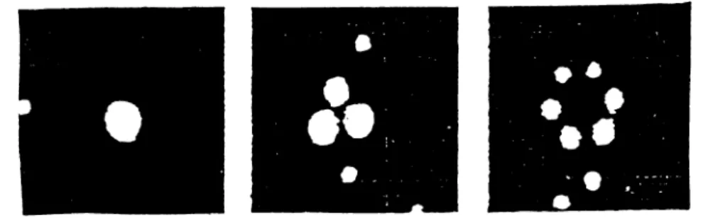
More recently Fink [47] reported a detailed study for the production of a mono-atomic tip. By using evaporation techniques he managed to form W
tips with a single atom on the surface. The Field Ion Microscopy patterns are shown in Figure 3.3. He also commented that it is possible to design tips by evaporating different kind of atoms onto the tip. But these studies are not extensively used in Scanning Tunneling Microscopy yet. Nevertheless, it is clear that the possibility of building mono-atom tips is very likely.
Figure 3.3: Field-ion pattern of mono-atomic tip
From left to right the first three atomic layers of the tip are shown. The layers are lifted by field evaporation. The figure is taken from Reference [47]
Even though the atomic structure of the tip can be analyzed, until now it was not possible to find its electronic structure in detail. The tip structure is very complicated, which makes a detailed account of the electronic structure difficult. This situation becomes a source of uncertainity in the tunneling mechanism. Nevertheless, the atomic structure by itself can give an idea about the possible model for the tip. In the present study a mono-atomic tip model has been used. For atomic scale resolution Park and Quate [14] remark that
3 .1 .2
T h e o ries for S can n in g T u n n elin g M icroscop y of
G ra p h ite
As a result of both its unusual electronic structure and appropriateness for the Scanning Tunneling Microscopy, graphite has drawn interests of both experimentalists and theoreticians. Since the first application of Scanning Tunneling Microscopy on graphite there have been a lot of suggestions about the mechanism of the anomalous tunneling current.
In 1985 Selloni et al. [48] calculated the energy band structure of graphite and found the corrugation maps for different finite biases. They used the spherical tip approximation of Tersoff and Hamann [33], and for non-zero biases used a triangular barrier for which the analytical tunneling current expression is known. They used empirical local pseudo-potential method to calculate the energy bands for a graphite slab, placed in a square potential well to approximate the surface potential. They found that by changing the bias one can tune any of the electron states to image. For infinitesimal bias, their charge density contour plots indicate that, the two basis atoms in the surface monolayer are not equivalent. However, this point was not recognized initially by Selloni et al. [48]. Corrugation amplitude for the on-top position and the hollow-site position is approximately 0.7 — 1.0 A. They also pointed out the possibility of observing surface states by the use of Scanning Tunneling Microscopy.
a graphite slab to investigate the Scanning Tunneling Microscopy data. Their results showed that the total charge density has a very small corrugation. In their analysis they found for the first time, that the A-type atoms have slightly smaller densities than B-type ones. They also found the local density of states at the Fermi energy. A typical local charge density plot of their results is shown in Figure 3.4. Their results for the corrugation amplitudes for this case increase up to 1.5 A between a B-type atom and the hollow-site, and are consistent with those of Selloni et al. [48]. However, they [26] observed a more pronounced difference, as large as 0.5 A, between the corrugations of different types of atoms compared to 0.05 A of Selloni et al. as shown in their figures. Batra and Ciraci [49] reported similar results in a study concerning with the tip-surface interaction in Scanning Tunneling Microscopy and Atomic Force Microscopy. Batra et al. [26] also commented that the huge corrugations and loss of trigonal symmetry for the experimental results can be due to a slip of one of the planes. Some of the figures in Marti’s work [12] resemble the charge densities obtained by the slipped planes. This shows that the slip plane possibility is a reasonable one.
Tersoff [50] connected the anomalous corrugation to the imaging of individual states. In 1986 he analyzed the unusual corrugations observed for the graphite and for charge-density waves in TaSe2. Using the tunneling current expression he and Hamann [33] derived, he concluded that for structures with point-like Fermi surfaces, small biases image only the Fermi level state. This
Figure 3.4: Local density of states for graphite slab
The density is calculated for a height 3.2 a.u. above the surface plane. The arrow indicates the direction on which density increases. The lateral positions are in units of
a. u. . The figure is taken from Reference [26].
conclusion implies that for some structures it is almost impossible to find the topography, just by looking at the tunneling images, since Fermi level state need not have to have any basic relation with the atomic structure. Therefore it should be clear that depending on the particular system used. Scanning Tunneling Microscopy can give information about both surface geometry and electronic structure.
Tersoff [50] used a single monolayer for the graphite surface, since the interlayer interactions are very small and do not have anything to do with the anomalous corrugation. He took the six smallest reciprocal lattice vectors and expanded the local density of states in terms of these. Using Equation 2.8 he
found for the tunneling conductance:
3
( = l n [ Y ^ siri^ Wn · ?f ] + Co (3.2)
n = l
where C = 2/i2T(, zt being the tip height, ff = kpp, Co = —In(cr) +
constant , this constant depending on the experimental and material
parameters, u) define the directions of the reciprocal lattice vectors, namely (0,1), (jV^, —5), and (—|V ^, —1). Using this six-plane-wave expansion he showed that there are nodes oi p{fo^EF) at the hollow site of the unit cell. Which should be clear from the discussion in Section 3.1.1.
This dip at the hollow site means an infinite corrugation, and by itself is an anomalous result. However Tersoff commented that this dip is smoothened for the graphite slab due to symmetry reduction as a result of interlayer interactions [50]. In addition tip wavefunction would have some components with non-zero angular momentum around the surface normal, which will couple with the surface and give rise to a small but non-zero tunneling current.
Tersoff also found that in the six-plane-wave approximation corrugation amplitude is independent of the tip height zt [50]. He stated that this property of graphite, while being not exact, is the reason for easy resolution of graphite surface. His results indicating that there are some examples for which Scanning Tunneling Microscopy images are not related to the topography, but are the images of individual states at Fermi level.
This anomaly for the huge corrugation amplitude in graphite is explained in terms of elastic deformations by Soler at al. [23] . They argued that the giant corrugations observed are due to the local elastic deformations, which in turn enhance the electronically based corrugation. In their experiments they observed voltage dependent corrugations and they concluded that for small tip heights the tip is practically in “physical” contact with the surface and “It
is then clear that the actual tip displacement cannot he solely a matter of the
electronically induced corrugation. They used the standard elasticity theory
to find the elastic force between the tip and the surface [23]. Their result shows that for large tip heights the force is attractive and for small heights it is repulsive. One can then qualitatively state that when the tip is on the hollow site, there will be a very small current between the tip and the surface. In order to keep the current constant the tip will move towards the surface, thus by deforming the surface like a membrane it will create a dip-like deformation on the surface. This will yield a height reading, very much below the actual tip-surface separation. When the tip is on the on-top site, there will be an attractive force between the tip and the surface and there will appear a bump on the surface. The height reading will give a value larger than the tip-surface separation. Combining these two effects one can say that there will be a giant corrugation which is not related to the electronic structure of the surface alone.
Using the local density of states formalism for the tunneling current in the geometry determined by the elastic force they obtained the corrugation
Figure 3.5: Corrugation amplitude as a function of tunneling current
The lines indicate the theoretical results. The circles, triangles and squares are experimental values. The figure is taken from Reference [23]
amplitude as a function of tunnel current. The result is shown in Figure 3.5. The agreement with experimental results is very good and on the physical basis there are reasons for the presence of this kind of mechanism. As a result of the loose interlayer binding the graphite surface is sufficiently soft for these kind of giant deformations. In addition being a semi-metal with zero energy gap, graphite can be inspected by Scanning Tunneling Microscopy only for very small tip heights, leading to a strong interaction between the tip and the surface.
Recently Ciraci and Batra [51] carried out calculations for the electronic structure of the combined tip and surface system. They found that the total energy results lead to a force regime similar to that of Soler et al. [23]. They concluded that for small tip heights the height of the barrier becomes smaller
and a chemical bonding between the tip and the surface becomes possible. For this case the system is short circuited to lead to the cease of tunneling.
The giant corrugation amplitude is not the only anomalous result of Scanning Tunneling Microscopy in graphite. Mizes et al. [52] recently investigated the reasons for the images with different geometries, but having the same period. Using the same argument as several other researchers [50], they neglected the effects of reciprocal wave-vectors with magnitudes greater than that of the smallest six vectors. This negiection resumes on the relation;
- I fc| P) = (3.3)
Therefore the decay rate of larger Fourier components is larger, and at large tip heights they will not contribute to the current. Mizes et al. [52] used a two atom tip, with a random phase difference between them. They found that the current is proportional to the sum of local densities of states at Fermi level, at the positions of the two tip atoms. Since the surface wavefunction is described by three Fourier components [50,52], the final result is the summation of two sine waves with a phase difference. They showed that by changing this phase several different patterns can be obtained as one observed in the experiment. These pattern differences have nothing to do with the structure of the surface, but is related to the structure and the orientation of the tip with respect to the surface.