Journal of Physics: Condensed Matter
PAPER
Effects of charging and perpendicular electric field
on the properties of silicene and germanene
To cite this article: H Hakan Gürel et al 2013 J. Phys.: Condens. Matter 25 305007
View the article online for updates and enhancements.
Related content
Enhanced reduction of graphene oxide by means of charging and electric fields applied to hydroxyl groups
H Hakan Gürel and S Ciraci
-Effects of charging and electric field on graphene functionalized with titanium
H Hakan Gürel and S Ciraci
-First-principles prediction of a new Dirac-fermion material: silicon germanide monolayer
Hongcai Zhou, Mingwen Zhao, Xiaoming Zhang et al.
-Recent citations
Strain and electric field induced
metallization in the GaX (X=N, P, As & Sb) monolayer
Bhagwati Prasad Bahuguna et al
-Functionalization of group-14 two-dimensional materials
Mariusz Krawiec
-Effect of charging on silicene with alkali metal atom adsorption
Manman Li et al
J. Phys.: Condens. Matter 25 (2013) 305007 (6pp) doi:10.1088/0953-8984/25/30/305007
Effects of charging and perpendicular
electric field on the properties of silicene
and germanene
H Hakan G ¨urel
1,2,3, V Ongun ¨
Ozc¸elik
1,2and S Ciraci
1,2,41UNAM-National Nanotechnology Research Center, Bilkent University, 06800 Ankara, Turkey 2Institute of Materials Science and Nanotechnology, Bilkent University, Ankara 06800, Turkey 3Technology Faculty, Department of Information Systems Engineering, Kocaeli University,
Kocaeli 41380, Turkey
4Department of Physics, Bilkent University, Ankara 06800, Turkey
E-mail:[email protected]
Received 17 March 2013, in final form 3 June 2013 Published 10 July 2013
Online atstacks.iop.org/JPhysCM/25/305007 Abstract
Using first-principles density functional theory calculations, we showed that electronic and magnetic properties of bare and Ti adatom adsorbed single-layer silicene and germanene, which are charged or subjected to a perpendicular electric field, can be modified to attain new functionalities. In particular, when subjected to a perpendicular electric field, buckled atoms have the symmetry between their planes broken, opening a gap at the Dirac points. The occupation of 3d orbitals of the adsorbed Ti atom changes with charging or applied electric field, inducing significant changes in magnetic moment. We predict neutral silicene uniformly covered by Ti atoms to become a half-metal at a specific value of coverage and hence allow the transport of electrons in one spin direction, but block the opposite direction. These calculated properties, however, exhibit a dependence on the size of the vacuum spacing between periodically repeating silicene and germanene layers, if they are treated using a plane wave basis set within periodic boundary conditions. We clarified the cause of this spurious dependence and show that it can be eliminated by the use of a local orbital basis set. (Some figures may appear in colour only in the online journal)
1. Introduction
When charged or subjected to an external electric field, two-dimensional (2D) materials show important modifications in electronic structure. In particular graphene, a single layer of honeycomb structure of carbon atoms, is a semimetal and has an ambipolar character with π and π∗ bands, which cross
linearly at the Fermi level. Depending on the polarity of the excess charge in graphene, the Dirac points shift the Fermi level up or down. For example, the excess electrons cause the Dirac points to dip below the Fermi level. This way, semimetal graphene changes into a metal. When electrons are depleted, the Dirac points move up and graphene becomes hole doped. Electric field applied perpendicular to graphene layers breaks the symmetry between the two sides of the plane of carbon
atoms. However, the π and π∗bands continue to cross. The effects of excess charge and perpendicular electric field on the electronic structure of graphene were investigated earlier [1].
The dependence of the electronic structure of silicene when charged or subjected to perpendicular electric field is also of current interest. The stability of this nanostructure in the buckled honeycomb geometry has been proven through ab initio phonon calculations and extensive high temperature, first-principles molecular dynamics simulations by Cahangirov et al [2]. Like for graphene, (in the absence of spin–orbit coupling) the π and π∗ like bands of 2D silicene cross each other linearly at the Fermi level leading to massless Dirac fermion behavior with a Fermi velocity vF ∼c/300 (c being the speed of light) and they exhibit an
J. Phys.: Condens. Matter 25 (2013) 305007 H H G¨urel et al
Interestingly, quasi-one-dimensional armchair nanoribbons of silicene were predicted to be semiconductors and they show a family behavior like graphene [2, 3]. The synthesis of single-layer silicene [5,6] which was achieved recently, has corroborated theoretical predictions by eliminating doubts about whether such a material can exist even though the parent silicon does not form a layered structure. Like silicene, germanene also displays similar properties. Both silicene and germanene lack the strong π–π interaction necessary for planar geometry, but they are stabilized through sp3 hybridization followed by sp2dehybridization [2,4] leading to buckling.
Normally, electric field applied perpendicularly to the silicene or germanene layers (E⊥) breaks the symmetry
between two Si or Ge layers formed by these atoms situated at the alternating corners of buckled hexagons. As a result, linearly crossing bands split to open a band gap. Such a gap opening did not occur in graphene because of the planar geometry of constituent carbon atoms. In fact, the gap openings of linearly crossing bands of silicene under E⊥ have been studied earlier by two papers [7, 8]. One of
them [7] carried out density functional (DFT) calculations within periodic boundary conditions (PBC) using a plane wave (PW) basis set and reported that the band gap depends on the vacuum spacing s between adjacent layers.
2. Methodology
In this paper, we investigated the effects of charging and applied perpendicular electric field on the electronic, magnetic and chemical properties of silicene and germanene by performing first-principles DFT spin-polarized and spin-unpolarized calculations using PBC within supercell geometry with varying vacuum spacing s. We used PW, as well as local, atomic orbital (AO) basis sets. First, we clarified how the effects of charging and perpendicular electric field calculated from the first-principles PW method can depend on the vacuum spacing s as an artifact of the method. Furthermore, we showed that this artifact can be eliminated if silicene or germanene, which are subjected to E⊥or charged
by excess electrons Q, are treated using the AO basis set. With the premises that silicene and germanene can attain new functionalities through the charging and the applied electric field, the present results will be crucial for future theoretical and experimental studies. In order to show the effects of external effects, such as E⊥ and Q, we did not consider the
spin–orbit coupling, which also gives rise to a small band opening. PW and local AO basis sets are used in numerical calculations through VASP [11] and SIESTA [12] packages, respectively.
The exchange–correlation potential is approximated by the generalized gradient approximation using the Perdew, Burke and Ernzerhof (PBE) functional [10]. Dipole corrections [13] are applied in order to remove spurious dipole interactions between periodic images for the neutral calculations. For all structures studied in this paper, the geometry optimization is performed by the conjugate gradient method, allowing all the atomic positions and lattice constants
to relax. The convergence for energy is chosen as 10−5 eV between two consecutive steps. In atomic relaxations, the total energy is minimized until the forces on atoms are smaller than 0.04 eV ˚A−1.
A basis set with kinetic energy cutoff of 500 eV and projector-augmented wave potentials [9] are used in the PW calculations [11]. In AO calculations [12] the eigenstates of the Kohn–Sham Hamiltonian are expressed as linear combinations of numerical atomic orbitals. A 250 Ryd mesh cutoff is chosen and the self-consistent calculations are performed with a mixing rate of 0.2. Core electrons are replaced by norm-conserving, nonlocal Troullier–Martins pseudopotentials [14]. The grid of k-points used is 19×19×1 for AO calculations and 12×12×1 for PW calculations, which are determined by a convergence analysis with respect to the number of grid points.
3. Results
Before we start to investigate the effects of charging on the electronic structure of silicene and germanene, we first examine the limitations of the PBC method, where two-dimensional silicene as well as germanene layers separated by large spacing s are repeated periodically along the z-axis. We carried out first-principles PW calculations as well as AO calculations and investigated the effect of charging on silicene and germanene layers. Throughout the paper, Q< 0 indicates the negative charging, namely the number of excess electrons per primitive cell (corresponding to the surface charge density
¯
σ = Q/A in C m−2, A being the area of the primitive cell);
Q> 0 indicates the positive charging, namely the number of depleted electrons per primitive cell; and Q = 0 indicates the neutral cell.
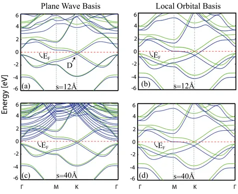
The calculated electronic structures of silicene and germanene are presented in figures 1and2. For the neutral case (Q = 0), the work function, i.e. the minimum energy that must be given to an electron to release it from the single layer, is the difference of the reference vacuum energy and Fermi level. The value of the work function extracted from the band structure is8 = 4.57 eV (8 = 4.37 eV for germanene). As seen, the electronic structures calculated using the PW and AO are similar. Minute differences originate from the different pseudopotentials used in calculations. Moreover, perfect convergence of different basis sets can be achieved only by using very large cutoff values.
The negative charging can lead to marked effects in the electronic structure of single-layer silicene and germanene. For charging with Q = −0.2 electrons per primitive cell, the energy bands calculated for the vacuum spacing s = 12 ˚A using the PW in figure1(a) and AO basis sets in figure1(b) are similar. The Dirac points dip below the Fermi level and the semimetallic silicene becomes a metal. A similar effect is seen also in the band structure of germanene in figure 2. However, when the same charged systems are treated with a relatively large vacuum spacing of s = 40 ˚A, the PW results dramatically deviate from the AO ones. Parabolic bands are lowered and eventually the Fermi level is pinned as shown in figure 1(c). Such a situation does not occur when the AO
Figure 1. Modification of the energy band structure of silicene when charged with Q = −0.2 electrons per primitive cell: (a) energy bands of neutral and charged cases calculated for s = 12 ˚A using a plane wave (PW) basis set are shown by green (light) and blue (dark) lines, respectively. Dirac points are lowered below the Fermi level upon charging. (b) The same system as in (a) is treated using the atomic orbital (AO) basis set. (c) Same as (a) except that s = 40 ˚A. Parabolic bands touching the Fermi level are due to the free electron like states confined to the quantum well centered at s/2 as described in figure3(a). (d) Same as (b) except that s = 40 ˚A. As seen, results obtained using AO calculations do not depend on s. The inset at the top shows the buckled honeycomb structure of the silicene with buckling1 = 0.45 ˚A.
J. Phys.: Condens. Matter 25 (2013) 305007 H H G¨urel et al
basis set is used. Hence, results obtained from AO calculations are independent of the size of the vacuum spacing as seen in figure1(d).
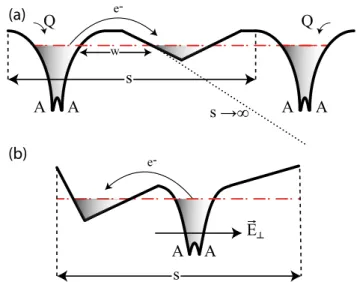
The cause of this spurious dependence of the vacuum size can be understood through the (x, y)-plane-averaged self-consistent field (SCF) electronic potential along the z-direction. A schematic description of the situation, which explains how the excess electrons for negatively charged silicene or germanene layers can spill into the vacuum region as a result of the above spurious effect, is shown in figure3(a). Earlier we made such an analysis by plane averaging the 3D, SCF one-electron potential of graphene [1]. Here the same situation is arising; as schematically described, ¯V(z) is lowered and passes through a minimum at the middle of the vacuum spacing. Normally, for Q = 0, ¯V(z) makes sharp dips at the atomic layers and rises and flattens at s/2. The maximum of ¯V(z) corresponds to the vacuum potential. However, in the actual case of a single silicene (or germanene) layer, which is charged with Q< 0, ¯V(z) passes through a maximum near the surface and goes to −∞ as z → ±∞ on both sides. Then, in view the 1D WKB approximation, the electrons in the silicene (or germanene) layer could have spilled to the vacuum only if they could tunnel across a wide triangular barrier. The width of the barrier, w, decreases with increasing negative charging. Under these circumstances, the spilling of electrons must have been negligibly low and hence excess electrons are practically trapped in the layer if the value of |Q| is not very high. However, when treated within PBC, ¯V(z) for periodically repeating silicene (or germanene) layers with a vacuum spacing s between them can show a dip reminiscent of a quantum well at the center of the spacing as shown in figure3(a). Under these circumstances, the Kohn–Sham Hamiltonian using the PW can acquire solutions in this quantum well, which are localized along the z-direction, but free electron like in the (x, y)-plane parallel to the Si planes. These states form the parabolic bands in the (kx, ky) plane as shown in figures 1(c) and 2(c). If the
quantum well dips below the Fermi level with increasing s or Q, excess electrons in silicene or germanene start to be accommodated in these 2D free electron like bands. This ends up with the spilling of excess electrons into the vacuum region. The amount of excess electrons spilled to the vacuum spacing increases with increasing s and also increases with increasing negative charging at a fixed value of s. The situation in figures1(c) and2(c), with the Fermi level pinned by the parabolic bands of electrons spilled to the vacuum for large s, is an artifact of the PBC and gives rise to the dependence on the size of the vacuum.
As for AO calculations, the spurious quantum well like structure at the middle of the vacuum spacing between the silicene or germanene layers in PBC is devoid of a basis set and hence cannot support the bound electronic states, since the local atomic orbitals are placed only at the atomic sites. This is why ¯V(z) calculated by the AO method does not accommodate excess electrons in its minimum between silicene layers and hence the parabolic bands seen in figures1(c) and2(c) do not appear in figures 1(d) and 2(d), when it is further lowered below the Fermi level with increasing s. The behavior of
Figure 3. (a) A schematic description of plane-averaged electronic potentials ¯V(z) explains how the excess electrons of silicene or germanene charged with Q< 0 can spill to the vacuum region, when treated using the PW within PBC. A stands for atomic planes. (b) Same for the electric field E⊥, exerted perpendicular to the
silicene and germanene planes. The vacuum spacing between the layers is denoted by s.
¯
V(z) in the proximity of the surface is similar to the actual case, where s → ∞. Accordingly, excess negative charge is prevented from spilling into the spacing between adjacent graphene layers, and hence remains in silicene as in the actual case consisting of one single silicene or germanene layer charged with Q< 0.
In contrast to the above shortcomings arising in the PW method in treating the negative charging Q< 0, results obtained by the AO and PW methods are in reasonable agreement for Q ≥ 0, since ¯V(z) passes through a maximum at the center of s between graphene layers. Accordingly, a method using PBC and a PW basis set is not affected significantly by the size of the vacuum spacing s if Q ≥ 0. For positive charging, the Fermi level shifts the Dirac points down and the material becomes hole doped and hence is metallized. In the case of E⊥, the mirror symmetry between the top
side and the bottom side of silicene is broken, and hence the plane-averaged electronic potential exhibits a sawtooth like variation in PBC. At high E⊥ and large s, a quantum well
like structure occurs at the lowered side of ¯V(z). When treated by the PW method, this quantum well like structure can dip below the Fermi level and hence electrons of silicene which can be accommodated in this quantum well end up with the electron spilling to the vacuum, resulting in a similar situation to that above for Q < 0. This situation is schematically described in figure 3(b). This is why the band gap opening under E⊥depends on s in DFT calculations using the plane
wave basis set [7]. As a matter of fact, in the band structure presented in figure 3(c) for the recent plane wave based study [7], at high E⊥ one sees a free electron like band
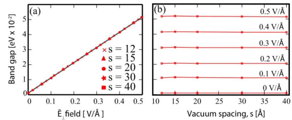
touching the Fermi level. However, for treatment by the AO method, calculated values of the band gap as a function of E⊥
fall on the same line as shown in figure 4(a). This is better seen in figure4(b) demonstrating that band gaps induced for
Figure 4. (a) Linear variation of band gap opening1E versus applied electric field E⊥for silicene. When obtained using AO, band gap
values calculated for various values of s fall on the same line. (b) Gap opening1E as a function of applied electric field E⊥calculated for
different vacuum spacings s. Gap openings induced by E⊥do not depend on the vacuum spacing s, when calculated using AO.
Table 1. Magnetic ground states (AFM: antiferromagnetic or FM: ferromagnetic) and magnetic moments inµBper Ti atom (i.e. per (2 × 2)
cell) calculated as a function of charging and applied perpendicular electric field. Calculations are performed in the (4 × 4) supercell of silicene and germanene having four uniformly adsorbed Ti atoms. E⊥(+1) denotes positive E⊥=1 V ˚A
−1
(directed towards the Ti atom) and vice versa for E⊥(−1). Q(+1 e) corresponds to the charging where one electron is removed from the (4 × 4) supercell and vice versa
for Q(−1 e).
E⊥(V ˚A −1
) or Q(e)
Silicene + Ti Germanene + Ti
Ground state Mag. moment (µB) Ground state Mag. moment (µB)
E⊥(+1) AFM 0.00 FM 2.50
E⊥(−1) FM 3.11 FM 2.39
Q(+1 e) FM 3.14 FM 2.25
Q(−1 e) FM 2.86 FM 2.14
Neutral FM 3.00 FM 2.06
different values of E⊥ are practically independent of s. The
behavior of the gap opening with applied E⊥in germanene is
similar to that for silicene.
Spin-polarized calculations indicate that the non-magnetic ground state of silicene and germanene is practically unaltered upon charging or under electric field. However, the permanent magnetic moment of a Ti atom adsorbed to silicene and germanene exhibits significant changes upon charging or under the electric field. However, it is argued that ordinary DFT may not be appropriate for treating the strongly correlated d orbitals, such as in adsorbed Ti atoms. Often approaches such as DFT + U are used to address this issue [15]. Surprisingly, in most cases concerning Ti adsorbed on Si and graphene surfaces, DFT has provided reasonable predictions. Earlier, we examined the effects of correlation by performing LDA + U calculations [15]. Since U parameters were not available for Ti adsorbed on Si surfaces, we carried out calculations by taking U as a parameter [16]. We also performed similar calculations for transition metal dichalcogenides, ScO2, NiO2 and WO2 in
single-layer honeycomb structure [17]. We found that in these studies up to high values of U our predictions obtained by DFT remained valid. Energetically, the most favorable bonding site of the Ti adatom on silicene and germanene is found to be the hollow site, above the center of the hexagon. We investigate the magnetic properties of Ti covered silicene and germanene using supercell geometry in different levels of coverage, since the resulting magnetic ground states depend on the Ti–Ti coupling and hence on the Ti atom coverage.
First, we consider the case of very weak Ti–Ti coupling by using uniform coverage in which one Ti adatom is adsorbed to each (4 × 4) supercell of silicene (germanene) corresponding to2 = 1/32 (i.e. one Ti atom per 32 Si (Ge) atoms) and leading to the Ti–Ti distance of 15.39 ˚A (16.06 ˚A). In the neutral case, both silicene and germanene have a spin-polarized, ferromagnetic (FM) ground state with a magnetic moment of µ = 2.44 µB/cell (i.e. per (4 × 4)
supercell). The magnetic moment of the spin-polarized state of silicene increases toµ = 3.00 µB/cell (µ = 2.55 µB/cell
for germanene) for Q = +1.0 e/cell. For the excess electronic charge of Q = −1.0 e/cell the magnetic moment increases to µ = 2.77 µB/cell (µ = 1.44 µB/cell for germanene).
The variation ofµ is due to the accommodation of different electronic charges of Ti 3d states for different values of Q. A similar effect can be generated also by the static electric field. Spin polarizations of Ti adsorbed silicene and germanene show also significant changes with applied electric field E⊥.
While their magnetic moments become unaltered for E⊥=
+1.0 V ˚A−1 (i.e. E⊥ is directed towards the Ti adatom),
they increase to µ = 3.55 µB/cell for E⊥= −1.0 V ˚A −1
. Apparently, either by charging of the Ti + silicene (Ti + germanene)(4 × 4) complex or by exerting an electric field, E⊥< 0, one can modify the occupations of 3d orbitals and
hence can change the net magnetic moment.
When a significant Ti–Ti interaction sets in, the magnetic ground states show interesting changes as presented in table1. We consider the case of significant Ti–Ti coupling by using
J. Phys.: Condens. Matter 25 (2013) 305007 H H G¨urel et al
uniform coverage in which four Ti adatoms are adsorbed to each(4 × 4) supercell of silicene (germanene) corresponding to 2 = 1/8 coverage and leading to a Ti–Ti distance of 7.69 ˚A (8.03 ˚A). This supercell geometry allows us to treat the antiferromagnetic (AFM) order. Similar to the case for coverage of 2 = 1/32, silicene and germanene have FM spin-polarized FM magnetic ground states at2 = 1/8, except in the case of the AFM ground state occurring under E⊥=
1 V ˚A−1. Also we predict that an external effect like Q or E⊥
causing charge depletion from the Ti adatom will give rise to an increase in the magnetic moment.
We predict that silicene uniformly covered with Ti atoms at2 = 1/8 is spin-polarized and has the permanent magnetic moment of µ = 3.0 µB and is a half-metal: namely it is
metal for one spin direction, but a semiconductor for the opposite spin direction. Accordingly, this material transports electrons only for one spin direction and can function as a spin valve. While silicene has an AFM ground state with zero net magnetic moment under E⊥=1 V ˚A
−1
, the ground state changes to FM when the direction of the electric field is reversed, causing charge transfer towards the Ti atom. Finally, it should be noted that the binding site and magnetic moments of the neutral case may show minute changes depending on the method of calculation.
4. Conclusions
In conclusion, single-layer silicene and germanene can attain useful functionalities upon charging and exposure to a perpendicular electric field. While charging maintains the symmetry between the two sides of the honeycomb structure, this symmetry is broken by the electric field perpendicular to the layer. As a result, linearly crossing bands split, where the band gap becomes linearly dependent on the value of the electric field. Also the work function and the binding energies of foreign adatoms become side specific. In particular, the occupations of 3d orbitals of transition metal atoms adsorbed to silicene or germanene can be modified by charging or by applying an electric field, which in turn, give rise to important changes in magnetic moments. We showed that the vacuum space which can affect the calculated properties of silicene under excess charge or electric field can be eliminated by using local orbital basis sets.
Acknowledgments
This work was supported by TUBITAK and the Academy of Sciences of Turkey (TUBA). Some of the computa-tional resources were provided by TUBITAK ULAKBIM,
High Performance and Grid Computing Center (TR-Grid e-Infrastructure) and UYBHM at Istanbul Technical Uni-versity through Grant No. 2-024-2007. Dr H H G¨urel acknowledges the support of TUBITAK-BIDEB.
References
[1] Topsakal M and Ciraci S 2012 Effects of static charging and exfoliation of layered crystals Phys. Rev. B85 045121 [2] Cahangirov S, Topsakal M, Akturk E, Sahin H and Ciraci S
2009 Two- and one-dimensional honeycomb structures of silicon and germanium Phys. Rev. Lett.102 236804 [3] Cahangirov S, Topsakal M and Ciraci S 2010 Armchair
nanoribbons of silicon and germanium honeycomb structures Phys. Rev. B81 195120
[4] Sahin H, Cahangirov S, Topsakal M, Bekaraoglu E, Akturk E, Senger R T and Ciraci S 2009 Monolayer honeycomb structures of group-IV elements and III–V binary compounds: first-principles calculations Phys. Rev. B 80 155453
[5] Vogt P, De Padova P, Quaresima C, Avila J, Frantzeskakis E, Asensio M C, Resta A, Ealet B and Le Lay G 2012 Silicene: compelling experimental evidence for graphenelike two-dimensional silicon Phys. Rev. Lett.108 155501 [6] Aufray B, Kara A, Vizzini S, Oughaddou H, Leandri C, Ealet B and Le Lay G 2010 Evidence of graphene-like electronic signature in silicene nanoribbons Appl. Phys. Lett.96 261905
[7] Drummond N D, Z´olyomi V and Fal’ko V I 2012 Electrically tunable band gap in silicene Phys. Rev. B85 075423 [8] Ni Z, Liu Q, Tang K, Zheng J, Zhou J, Qin R, Gao Z, Yu D
and Lu J 2012 Tunable bandgap in silicene and germanene Nano Lett.12 113
[9] Blochl P E 1994 Projector augmented-wave method Phys. Rev. B50 17953
[10] Perdew J P, Burke K and Ernzerhof M 1996 Generalized gradient approximation made simple Phys. Rev. Lett. 77 3865
[11] Kresse G and Furthmuller J 1996 Efficient iterative schemes for ab initio total-energy calculations using a plane-wave basis set Phys. Rev. B54 11169
[12] Soler J M et al 2002 The SIESTA method for ab initio order-N materials simulation J. Phys.: Condens. Matter14 2745 [13] Markov G and Payne M C 1995 Periodic boundary conditions
in ab initio calculations Phys. Rev. B51 4014
[14] Troullier N and Martins J L 1991 Efficient pseudopotentials for plane-wave calculations Phys. Rev. B43 1993 [15] Dudarev S L, Botton G A, Savrasov S Y, Humpreys C J and
Sutton A P 1998 Electron energy-loss spectra and the structural stability of nickel oxide: an LSDA + U study Phys. Rev.B57 1505
[16] Durgun E, Cakir D, Akman N and Ciraci S 2007 Half-metallic silicon nanowires: first-principles calculations Phys. Rev. Lett.99 256806
[17] Ataca C, Sahin H and Ciraci S 2011 Stable, single-layer MX2
transition-metal oxides and dichalcogenides in a honeycomb-like structure J. Phys. Chem. C 8983–99