' U M
Ü C T O R D O Î
τ γ iw jw jA T W ’-Î’ CÎ.'Î'fô .
SU3M ITtS0 ТО THE öEFÂSıTlâEMT OF PHlfilCS
Ш THE IHSTITUTE' OF Ш О Ш Ш Ш й А Ш . BCIEHCS
HiuJ^Aa 4ittaiP 4IU JUtif я 4ttw timiM '«b-jii ar дті«ь^ЛѴ &wsn» Jä лй
Ш FÁHTIAI FüLfІЕШЖВІТ ÖF TEE EiaOISSMEIITS
tiXjfiü
I aü±i W:aiuaiSÄ Oie
■:5/r ü îİ'î'-:îî5'P ífíi'rf 5 . Л л и Д '· - ‘ÍW?'*.« ΙΙί^<^>Μ<«Λ*.·Λ;4ΐί&4ΐ •«to/BÄUt '! ‘»' ,/■ .И^чЧ ’ '<»·'·* ,,·'’ . ’“ i ί ψ - Ο ό
'S13
iâBô
^Κ·- '! ■·» rr '^··Ir X Ім/.|· «w*' '^Û irf\«WIT. 'lU^'
F A B R IC A T IO N A N D C H A R A C T E R IZ A T IO N
OF S E M IC O N D U C T O R D O U B L E
Q U A N T U M W E L L D IO D E LASER S
A THESIS
SUBMITTED TO THE DEPARTMENT OF PHYSICS AND THE INSTITUTE OF ENGINEERING AND SCIENCE
OF BILKENT UNIVERSITY
IN PARTIAL FULFILLMENT OF THE REQUIREMENTS FOR THE DEGREE OF
MASTER OF SCIENCE
B y
Bülent Erol Sağol
November 1998
Tft •1=fco
•£
1 Ъ
-isas ь4 5 1
q (ОI certify that I have read this thesis and that in my opinion it is fully adequate, in scope and in quality, as a dissertation for the degree of Master of Science.
Asst. Prof. Mi Serp^guzel (Supervisor) I certify that I have read this thesis and that in my opinion it is fully adequate, in scope and in quality, as a dissertation for the degree of Master of Science.
Assoc. Prof. EKmdr Ozbay
I certify that I have read this thesis and that in my opinion it is fully adequate, in scope and in quality, as a dissertation for the degree of Master of Science.
Prof. Çiğdem Ercelebi
Approved for the Institute of Engineering and Seience:
Prof. Mehmet Bar ay.
Abstract
FABR ICATIO N A N D C H A R A C T E R IZ A T IO N OF
SE M IC O N D U C T O R DOUBLE Q U A N T U M WELL
DIODE LASERS
Bülent Erol Sağol
M. S. in Physics
Supervisor: Asst. Prof. Ali Serpengüzel
November 1998
In this thesis, semiconductor double quantum well, Fabry-Perot and half ring hisers were fabricated, and these devices were operated and characterized at room temperature.
The lasers were fabricated using GaAs/AlGaAs double quantum well wafers, and processed in order to produce 4^m wide, l/im-4/im high mesas for optical confinement. This mesa isolation was done by means of wet and dry etching techniques. Fabrication of Fabry-Perot lasers was completed after Si02 insulation, p-contact and n-contact metalizations, thinning, and dicing. Similar fabrication techniques were applied to produce ring lasers coupled to Fabry-Perot cavities, with various diameters ranging from 50 to 1400//m.
Device characterization was done by means of photoluminescence, current- voltage, current-power measurements, and electroluminescence. Photolumi nescence was used for checking the lasing wavelength. Current-voltage and current-power measurements were done to investigate the serial resistances, threshold currents, and differential quantum efficiencies of the fabricated devices
with various cavity lengths. From these measurements, the threshold current densities, the internal quantum efficiencies, and the internal net optical losses were obtained. Finally, electroluminescence was used to obtain the lasing spectra, and from this, the free spectral range of the Fabry-Perot and ring lasers were measured.
K e y w o r d s : Semiconductor diode lasers, quantum well, Fabry-Perot, lasing spectrum, threshold current, gain bandwidth, ring laser
özet
ç i f t
K U V A N T U M K U Y U L U YA R IİLE TK E N
LAZERLERİNİN Y A P IM I V E İNCELENM ESİ
Bülent Erol Sağol
Fizik Yüksek Lisans
Tez Yöneticisi: Yard. Doç. Dr. Ali Serpengüzel
Kasım 1998
Bu tez çalışmasında, çift kuvantum kuyulu yarıiletken Fabry-Perot ve yarım halka lazerleri üretildi, ve oda sıcaklığında çalıştırılıp, aygıt ölçümleri yapıldı.
Bu lazerlerin yapımı GaAs/AlGaAs çift kuvantum kuyulu örnekler üzerinde gerçekleştirildi, ve öncelikle optik hapsetme sağlamak için, ıslak ve kuru aşındırma yöntemleri ile 4^m genişliğinde ve l/im-4/im yükseklikte platolar üretildi. Daha sonraki adımlarda bu örneklere SİO2 yalıtımı, p-kontak ve n- kontak metalizasyonları uygulandı, örnekler inceltildi ve kesildi. Buna çok yakın bir üretim yöntemi, Fabry-Perot kavitelerine bağlanan 50 ile 1400/im arasında değişen çaplardaki halka lazerleri için uygulandı ve bunlar için de aynı ölçümler yapıldı.
Aygıtların incelenmesi, fotoışıma, akım-voltaj, akım-güç ölçümleri, ve elektroışıma ile yapıldı. Fotoışıma lazer dalgaboyunun saptanması için kullanıldı. .Akım-voltaj, akım-güç ölçümleri değişik boylardaki aygıtların seri dirençlerini, eşik akımlarını ve diferansiyel kuvantum verimliliklerini incelemek için yapıldı. Bu ölçümlerden, eşik akım yoğunlukları, içsel kuvantum verimlilikleri, ve içsel net optik kayıpları elde edildi. Son olarak, lazer tayfı elde etmek için
elektrolşıma kullanıldı, ve buradan Fabry-Perot ve halka lazerlerinin serbest tayf aralıkları ölçüldü.
A n a h ta r
sözcü k ler: Yarıiletken diyot lazerleri, kuvantum kuyusu, Fabry-Perot, lazer tayfı, eşik akımı, kazanım bant aralığı, halka lazeri
Acknowledgement
I would like to express my deepest gratitude to Asst. Prof. Ali Serpengiizel for his supervision in this research, as well as for his understanding and help.
I would like to thank Talal Azfar, our good old process engineer Murat Güre, and Joan Carson from Glasgow University for their help in semiconductor laser fabrication. Special thanks to Alpan, Hüseyin, Selim, and Güngör Bey for their support in characterization.
I would like to thank Assoc. Prof. Ekmel Ozbay, Saiful Islam, and Erhan Ata for introducing me to the experimental device physics. Prof. Cemal Yalabık, on the behalf of the Physics Department, for my education, and Prof. Çiğdem Erçelebi for the helpful discussions.
I would also like to thank Bilkent University, Glasgow University, The Scientific & Technical Research Council of Turkey (TÜBİTAK), and the British Council for sponsoring my research.
And of course, very very special thanks to my dearest friends Kaan and Alpan for their sweet existence.
Vielen Dank TMuti, CVati, und CErtan! Vielen Dank fiir Eure anhaltende Unterstützung.
Contents
Abstract i Özet i Acknowledgement i Contents i List of Figures iv List of Tables vi 1 Introduction 1 1.1 L a s e r s ... 1 1.2 Semiconductor Diode L a s e r s ... 21.3 Quantum Well Lasers... 4
1.4 Ring L a s e r s ... 5
2 Semiconductor Laser Theory 7 2.1 Operation of L asers... 7
2.1.1 Stimulated and Spontaneous Emission 7 2.1.2 Population In v e rs io n ... 9
2.1.3 Energy Levels of Lasers... 9
2.1.4 Resonant C avities... 11
2.2.1 Semiconductor Properties 13
2.2.2 Light Emission at .Jun ctions... 14
2.3 Quantum Well Lasers... 16
2.3.1 Double Heterostructures... 17
2.3.2 Quantum Well S tru ctu re... 18
2.4 A Phenomenological Approach to Diode Lasers ... 20
2.4.1 Carrier Generation and Recombination in Active Regions . 20 2.4.2 Spontaneous Photon Generation and L E D s ... 22
2.4.3 Photon Generation and Loss in Laser C a v itie s ... 23
, 2.4.4 Basic Current Power Characteristics 24 3 Design and Fabrication 26 3.1 Mask D esign... 26
3.2 Wafers and Sample Cleavage... 28
3.3 Sample Cleaning and Cleanliness 32 3.4 Lamella Sticking 33 3.5 P h otolithography... 34
3.6 Oxygen A s h i n g ...^ ... 35
3.7 Mesa E t c h in g ... 36
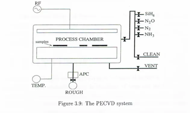
3.8 Plasma Enhanced Chemical Vapor Deposition ( P E C V D ) ... 38
3.9 PECVD L ift-O ff... 39 3.10 p-Contact M etalization... 40 3.11 p-Contact L ift-O ff... 42 3.12 p-Contact A n n e a lin g ... 43 3.13 T h in n in g... 43 3.14 n-Contact M etalization... 43 3.15 n-Contact A n n e a lin g ... 44 3.16 D i c i n g ... 44 3.17 Detailed Process L a y o u t ... 44
4 Characterization and Results 51
4.1 Diode Laser Parameters 51
4.2 E.xperimental S e t -U p ... 52 4.3 Photoluminescence Spectrum 53 4.3.1 Experimental Method 54 4.4 Current-Voltage C haracteristics... 55 4.5 Current-Power Characteristics... 57 4.5.1 Threshold C u r r e n t ... 58
4.5.2 Differential Quantum E fficie n cy ... 60
4.5.3 Internal Parameters: {ai) and t]i... 61
4.6 Electroluminescence S p ectru m ... 62
4.6.1 Free Spectral Range 63 4.6.2 Quality Factor... 65
4.6.3 Temperature Dependence of EL S p e c t r u m ... 65
4.7 Ring L a s e r s ... 67
5 Conclusion 72
List of Figures
2.1 The two level energy s y s t e m ... 8
2.2 The four level laser energy levels... 10
2.3 The Fabry-Perot resonator and its transmittance spectrum . . . . 12
2.4 The p-n junction as a simple semiconductor l a s e r ... 15
2.5 Light output as a function of current and w a v elen g th ... 16
2.6 Structures of two typical QW (therefore DH) l a s e r s ... 17
2.7 Band structure of a GRINSCH laser... 19
3.1 The layers of a 400/im diameter ring laser 27 3.2 The design of a 400^m diameter ring l a s e r ... 27
3.3 An array of 400//m diameter ring la se rs... 28
3.4 The organization of laser a r r a y s ... 29
3.5 The photomask l a y o u t ... 29
3.6 (100) p-type wafer co n v e n tio n ... 30
3.7 The band diagram and energy levels of the GRINSCH structure . 31 3.8 The epitaxial layers of the DQW GRINSCH structu re... 31
3.9 The PECVD s y s t e m ... 38
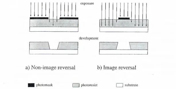
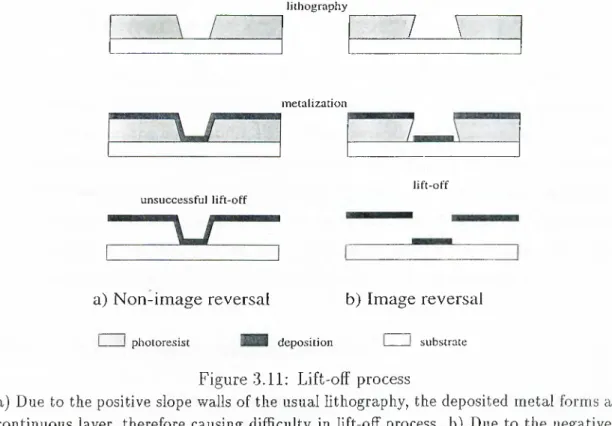
3.10 The image reversal lithography 41 3.11 Lift-off process ... 42
3.12 The most critical fabrication step s... 47
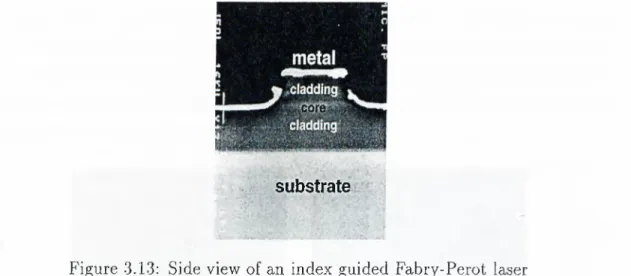
3.13 Side view of an index guided Fabry-Perot la se r... 48
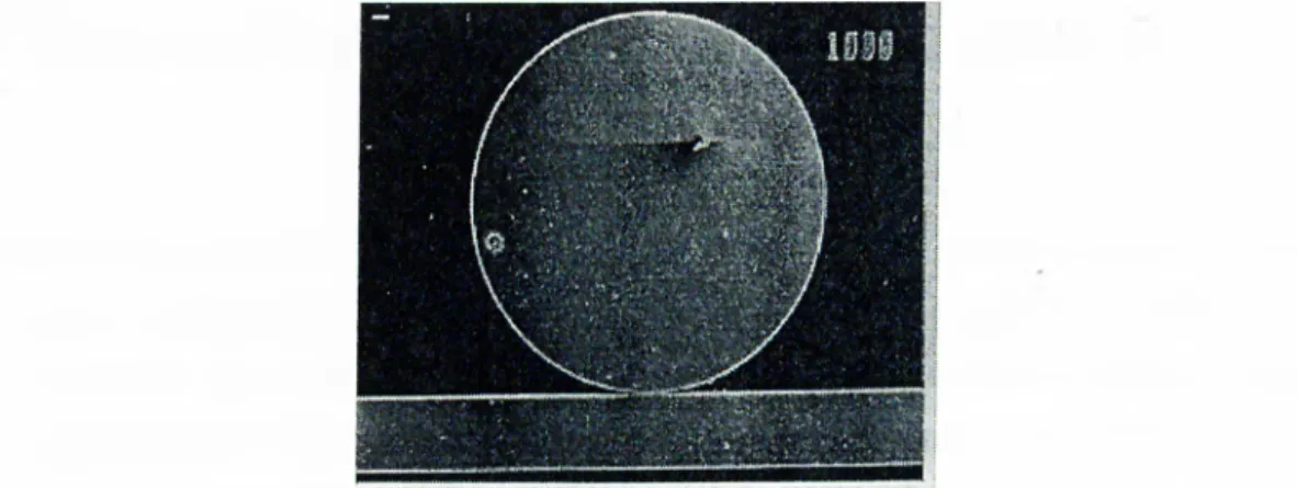
3.14 Top view of a 300/im diameter ring resonator 48 3.15 Dry etched mesas for the ring lasers... 49 3.16 Top view of a 1000//m diameter dry etched ring laser 50
4.1 The characterization set-up ... 52
4.2 Photoluminescence spectrum of the DQVV wafer at 3 0 0 K ... 55
4.3 Current-Voltage characteristics 56 4.4 Current-power ch a ra cteristics... 57
4.5 Current-power dependence of FP lasers for various cavity lengths at room tem p era tu re... 58
4.6 Infinite length threshold current density at room temperature as a benchmark... 59
4.7 Differential quantum efficiency of FP lasers... 60
4.8 The graph of inverse differential quantum efficiency versus cavity l e n g t h ... 62
4.9 Diode laser EL spectrum obtained by a CCD camera. T=75K 63 4.10 Free spectral range measurement of a room temperature diode laser, whose cavity is around 1 m m ... 64
4.11 Free spectral range of Fabry-Perot la s e r s ... 65
4.12 The lasing spectrum of lasers at various tem peratures... 66
4.13 The peak wavelength versus tem perature... 67
4.14 A room temperature 1.4mm diameter half ring la s e r... 68
4.15 Room temperature IP of a half ring la s e r ... 69
4.16 The modes of Fabry-Perot laser at room tem peratu re... 70
4.17 The whispering gallery modes of the room temperature half ring l a s e r ... 71
List of Tables
1.1 Important lasers and their operating wavelengths(nm)... 3 3.1 Oxygen ashing r e c ip e ... 36
3.2 PECVD recipe 39
4.1 Basic laser p a ra m e te rs... 52 4.2 The structure of the QT1071 DQW w afer... 68
Chapter 1
Introduction
The laser sits near the top of any list of the great inventions of the last half of the twentieth century. Together with the satellite, the computer and the integrated circuit, it is a symbol of high technology. Laser technology is both fascinating in itself and an important tool in fields from medicine to communications. Lasers can send signals through miles of fiber-optic cable, print computer output, read printed codes in the supermarket, diagnose and cure disease, cut and weld materials, and make ultra precise measurements. By the help of the laser light we can record three dimensional holograms, spot flaws in a centuries old painting, or play crystal clear digital music recorded on a compact disc.
1.1
Lasers
The word laser was coined as an acronym, for Light Amplification by the Stimulated Emission of Radiation. The word tells us, that laser light is a special light, which is emitted by stimulation, unlike the ordinary light.
Albert Einstein was the first to suggest the existence of stimulated emission in a paper published in 1917. However, for many years physicists thought that atoms and molecules always were much more likely to emit light spontaneously, and that stimulated emission thus always would be much weaker. It was not until after World War II, that physicists started to make stimulated emission
dominate.
The first to succeed was Charles H. Townes, who worked with microwaves, which have much longer wavelengths than the visible light. He built a device which he called m aser for Microwave Amplification by the Stimulated Emission of Radiation. He thought of the concept in 1951 at Columbia University, but the first maser was not completed until a couple of years later.
The key concepts about lasers emerged about 1957. Townes and Arthur Schawlow, then at AT&T Bell Laboratories, wrote a long paper outlining the conditions needed to amplify stimulated emission of visible light waves. At about the same time Gordon Gould, then a 37 year old graduate student, was writing similar ideas in a series of notebooks. Townes and Schawlow published their ideas in Physical Review Letters, but Gould filed a patent application.
Three years later, on May 16, 1960, Theodore Maiman built the first laser, using a synthetic ruby, two mirrors, and a flash lamp. This first ruby laser which operated at 694 nm, opened the way for various kinds of lasers, with various medium materials and operating wavelengths. In 1964, Townes and two Soviet maser pioneers, Nikolai Basov and Aleksander Prokhorov, shared the Nobel prize in physics for their pioneering work on the laser/maser principle.
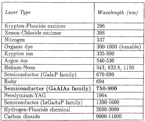
Lasers take many different shapes and many different properties, such as operating wavelength, output power, duration of emission, beam divergence, coherence, efficiency, and power requirements. In Table 1.1, some important lasers and their operating wavelengths are listed.
1.2
Semiconductor Diode Lasers
CHAPTER 1. INTRODUCTION 2
The roots of semiconductor laser technology go back to the 1950s, when the semiconductor physics was new. As far back as 1953, noted physicist .John von Neumann considered the possibility of light amplification by stimulated emission in semiconductors, but he never formally proposed the idea. In 1957, Yasushi Watanabe and Jun-ichi Nishizawa applied for a Japanese patent on a semiconductor maser concept. The most detailed proposals for semiconductor
CHAPTER 1. INTRODUCTION Laser Type Krypton-Fluoride excimer Xenon-Chloride excimer Nitrogen Organic dye Krypton ion Argon ion Helium-Neon
Semiconductor (GalnP family) Ruby
Semiconductor (GaAlAs family) Neodymium; YAG
Semiconductor (InGaAsP family) Hydrogen-Fluoride chemical Carbon dioxide Wavelength (nm) 296 308 337 300-1000 (tunable) 335-800 540-530 543, 632.8, 1150 670-680 694 750-900 1064 1300-1600 2600-3000 9000-11000
Table 1.1: Important lasers and their operating wavelengths (nm)
lasers emerged in 1961 from Nikolai Basov’s group at Lebedev Physics Institute in Moscow.
In 1962, four independent groups in the United States succeeded in making semiconductor lasers within weeks of each other: (the winner was Robert N. Hall of General Electric Research and Development Laboratories in Schenectady, NY.) Those lasers stimulated tremendous interest, but they only worked when high current pulses passed through them, and they required cooling down to 77K.
Modern semiconductor diode lasers incorporate a heterostructure in which the active layer is surrounded by a higher bandgap material. The heterostructure laser concept was suggested in 1963 by H. Kroemer^ in the U.S. and by R.F. Kcizarinov and I. Alferov^ in the former Soviet Union. In 1967, .J.M. Woodall
et al? of IBM succeeded in growing heterostructures of GaAs and AlGaAs by liquid phase epitaxy (LPE). By 1970 Alferov’s group'* and I. Hayashi and M.B. Panish at AT&T Bell Laboratories® had demonstrated double heterostructure Icisers continuously operating at room temperature.
CHAPTER 1. INTRODUCTION
1.3
Quantum W ell Lasers
Quantum well lasers have evolved out of the traditional double heterostructure semiconductor lasers, which provided good confinement for carriers and light. A need for even better localization of carriers and the technological developments enabling the fabrication of high quality, ultra thin semiconductor layers, paved the way to the realization of quasi two dimensional electronic structures in semiconductors. The quantum well structure provided a control over emission wavelength of the lasers by adjusting the thickness of the well layer, and offered reduced density of states in the conduction and valence bands, compared to the bulk semiconductors.*^
In March 1974, Chang, Esaki, and Tsu submitted a paper on the resonant tunneling through levels of quantum wells.^ This publication marks the first experimental demonstration of quantum well physics in heterostructures. The high gain of quantum well structures helped in fabricating devices with lower threshold current densities and improved the quality of semiconductor lasers. The first observation of quantum well laser operation was made by J.P. van der Ziel et al.^ in 1975. These first QW lasers were pumped optically and they operated at 15 K.
In November of 1977, Dupius, Dapkus and Holonyak submitted a paper, first reporting the demonstration of room temperature quantum well injection laser.^ It had a single 200A QW and a threshold current of about 3 k A /c m “^ at 300 K when pulse operated. In June and October 1978, they demonstrated the first report of cw operation of single quantum well (SQW) and multiple quantum well (M QW ) l a s e r s . T h e lowest threshold current was 1660 A/cm^, and the highest external differential quantum efficiency was 85%.
In this time period, the growth of lasers by MBE gradually improved, cind the first cw injection laser made by MBE was achieved by Cho et alH in December 1975. A great improvement in MBE grown lasers resulted from the research of W .T. Tsang starting from 1978. In 1982 Tsang^^ showed, that lasers with threshold current densities as low as 160 A/cm^, with internal
quantum efficiencies of up to 95% and with internal loss as low as 3cm~^ can be manulactured, with an introduction of graded index waveguide for separate optical confinement (GRINSCH) design. This landmark paper by Tsang demonstrated the advantage of quantum well lasers over conventional bulk active layer lasers in achieving low laser threshold. This started a steady growth in the popularity of quantum well lasers, which is still continuing.
CHAPTER 1. INTRODUCTION 5
1.4
Ring Lasers
In conventional semiconductor lasers, cleaved crystal facets are usually used as reflectors. Since a cleaved facet is flat to an atomic scale, and is formed by the simple procedure of cleaving, it is a useful and effective reflector for semiconductor lasers. However, it is difficult to integrate monolithically other light wave elements with a semiconductor laser of this kind, because the semiconductor is discontinuous at the cleaved facet. Therefore, the cleaved faces can not be used as they are in Fabry-Perot lasers. Thus, in order to fabricate p h o to n ic in teg ra ted circu its or devices including semiconductor lasers, it is necessary to fabricate reflectors or resonator’s by means of other methods. As one of the best solutions to this problem, ring lasers have been studied.
The first discussion of waveguiding along a curved boundary dates back to 1912, when Lord Rayleigh observed the w h isp erin g gallery guiding effect in St. Paul’s c a t h e d r a l.T h e first applications for curved waveguides were done in microwave technology in the 1930’s and 1940’s. Towards the end of 1960’s, curved wave guides were considered for optical applications, essentially scaled down versions of their microwave counterparts.
A half ring semiconductor laser was first realized in 1970 in a zinc diffused GaAs homoj unction laser. A fully circular semiconductor laser, electrically pumped, but without an output waveguide, was first demonstrated in 1977, where the operation was monitored from the scattered light off the sidewalls.
The first ring laser involving a Y-junction was recorded in 1 9 8 0 , but the concept of half ring and quarter ring resonators was further pursued to avoid
CHAPTER 1. INTRODUCTION
complications arising from outcoupling via the Y-junction. A few years later, a more detailed investigation of different laser geometries and fabrication issues was p u b lis h e d ,b u t the ring lasers were still regarded impractical due to their high threshold current (> 100mA) and the consequently arising requirement of pulsed operation. As materials and technology improved further, the first cw operation of full ring lasers was demonstrated in 1990.^^ In the following years, various output coupling techniques were investigated including Y-junctions, directional couplers, and MMI (multimode interference) couplers.^^“^®
Chapter 2
Semiconductor Laser Theory
2.1
Operation of Lasers
The word laser was coined as an acronym, for light amplification by the stimulated emission of radiation. The word tells us that laser light is not an ordinary light, from the sun or from a fluorescent light bulb, which is emitted spontaneously, when atoms or molecules get rid of excess energy by themselves. It is a very special light, because it occurs when an atom or molecule holds onto excess energy until it is stimulated to emit it as light.
2.1.1
Stimulated and Spontaneous Emission
For the sake of simplicity let us consider an atom having only two energy levels, an upper level E2 and a lower level Ei, as shown in Figure 2.1. Under normal circumstances the atom will be in the lower level as physical systems tend to the lowest possible energy state. If the atom in the lower level is exposed to radiation of frequency V2 1, where
= E2 — E\
h
(
2
.
1
)
then a high probability that it will absorb a photon and be excited to the upper level E2. This process is referred to as stim u lated a b sorp tion as the incident
CHAPTER 2. SEMICONDUCTOR LASER THEORY
light energy is necessary for the process to occur (Figure 2.1(b)). Usually within a few nanoseconds, after being excited to the higher energy level the atom will emit a photon of energy hv^x = E2 — Ei and return to the lower level. In 1917,
Einstein showed that the emission process can occur in two quite distinct ways. As with the absorption process, the emission process can be stimulated or it .can occur entirely spontaneously as illustrated in Figures 2.1(c) and (d).
-E,
(a)
E2
(c)
Figure 2.1: The two level energy system
(a) a two level energy system, (b) stimulated absorption, (c) stimulated emission and (d) spontaneous emission. The black dot indicates the energy state of the atom before absorption or emission event.
There are two very important points concerning stimulated emission upon which the properties of laser light depend. First, the photon produced by stimulated emission has the same energy, and therefore the same frequency as the stimulating photon. Second, the light waves associated with the two photons are in phase and have the same state of polarization. This means that if an atom is stimulated to emit light energy, the wave representing the stimulated photon adds to the incident wave on a constructive basis, thereby increiising its amplitude. We then have the process of light amplification by stimulated emission of radiation.
CHAPTER 2. SEMICONDUCTOR LASER THEORY
2.1.2
Population Inversion
The problem with stimulated emission is that it doesn’t work well under thermodynamic equilibrium, at which the atoms and molecules tend to be at their lowest possible energy levels. This tendency of atoms and molecules to drop to lower energy levels creates a problem in what is called p o p u la tio n , the number of atoms or molecules at each energy level. The ratio of the numbers of atoms or molecules in states 1 and 2 in thermodynamic equilibrium is given by the Boltzman distribution
_ ^-{E2-Ei)/kT
N, (2.2)
At room temperature, this ratio is quite small for transition energies corresponding to optical wavelengths. That means that in thermodynamic equilibrium, virtually all the atoms or molecules are in the ground state for a visible wavelength transition, and this makes stimulated emission difficult.
But there is a way to make stimulated emission dominate. If more atoms are in the excited state than in the lower level, photons are more likely to stimulate emission than be absorbed. Such a condition is called a p o p u la tio n inversion, because it is the reverse of the normal situation, where more atoms are in lower levels than in higher levels. When there is population inversion, stimulated emission can produce a cascade of light.
2.1.3
Energy Levels of Lasers
Creation of population inversions is very crucial in operation of a laser. If there are more atoms or molecules in the upper level, there are more emitters than absorbers, thus a photon with the transition energy is likely to encounter an excited state and stimulate emission before it is absorbed.
The standard way to produce a population inversion is by putting energy into the laser medium to excite atoms or molecules to higher energy levels. This excitation of the laser medium is called p u m p in g, which can be done optically, electrically, or by other excitation methods.
CHAPTER 2. SEMICONDUCTOR LASER THEORY 10
These excitation techniques won’t work unless atoms or molecules have the right energy-level structure. Normally excited states have short lifetimes and release their excess energy by spontaneous emission very rapidly in nanoseconds. Therefore to produce population inversion, longer lived excited states are needed, and such states do exist. They are called m eta stable levels, because they are unusually stable on an atomic time scale, lasting for microseconds or even for milliseconds. They are very important in laser physics, because they make the best kind of upper laser level.
highly excited level
upper level
Population Inversion
between these states
lower level
natural depopulation
ground state
Figure 2.2: The four level laser energy levels
It is impossible to produce population inversion in a two level system, because the upper and lower states cancel eachother with zero gain. Practical laser systems involve three, four, or more energy levels, depending on how the energy is transferred. The simplest type of energy-level structure is the th ree-lev el laser, (like Maiman’s ruby l a s e r ) , w h i c h consist of a highly excited level, a meta stable upper level, and the ground state as the lower level. Although the system works, it is not ideal. One problem is that the ground state is also the lower laser level. To produce a population inversion, one must a put majority
CHAPTER 2. SEMICONDUCTOR LASER THEORY 11
the atoms to the upper level, with an intense burst of energy. The population inversion is very difficult to sustain while the atoms alwciys tend to be at their ground states. Therefore the three-level lasers operate in pulsed mode.
Most practical lasers involve at least fou r levels as shown in Figure 2.2. As in the three level laser, the excitation energy raises the atom or molecule from the ground state to a short-lived highly excited level. The atom or molecule then drops quickly to a meta stable upper level. The laser transition takes the atoms or molecules to a lower state, but not all the way to the ground state in a single step. After they drop to the lower level, the atoms or molecules eventually lose the rest of their excess energy by spontaneous emission or other processes and drop to ground state.
Close inspection of the operation of real lasers, reveals that the energy level structures are more complex. Excitation is not always to a single high level, it may be to a group of levels, all of which decay to the same upper level.
2.1.4
Resonant Cavities
A population inversion is not all it takes to make a laser device. A hot blob ol gas with an inverted population, like a cosmic maser, emits light in every direction. The light may be stimulated emission, and it may be at a single wavelength, but it is not concentrated in a laser beam. To extract energy efficiently from a medium with a population inversion, and make a laser beam, you need a reson an t cavity that helps build up stimulated emission using feedback, i.e., reflecting some of it back into the laser medium.
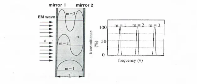
In most situations the overall amplification is increased by placing highly reflecting mirrors (reflectance approaching 100%) at each end of the medium. The optical beam then bounces back and forth through the medium, perhaps as many as hundred times (depending on the quality factor of the cavity), thereby increasing the effective length of the medium. The mirrors form an optical cavity or resonator, often called a F a b ry -P erot reson ator, and together with the active medium constitute an optical oscillator rather than an cxmplifler. There
CHAPTER 2. SEMICONDUCTOR LASER THEORY 12
are many kinds of resonators, for example large radius, confocal, hemispherical mirrors, or ri mirror 1 mirror 2 100 (O o C/3 50 C S 0 ...m.; = .l ...m = .2 ....m.)p . .. .
/ 1
/
, frequency (v)Figure 2.3: The Fabry-Perot resonator and its transmittance spectrum For laser oscillations to occur, a wave within the cavity must replicate itself cvfter two reflections, so that the electric fields add in phase. In other words the mirrors form a resonant cavity and standing wave patterns are set up in exactly the same way as standing waves develop on a string or within ah organ pipe (see Figure 2.3). The lowest mode of standing waves is when L=A/2, where L is the cavity length and A is the wavelength. Hence, for laser oscillation, the mth mode has to satisfy the condition:
,
A
L = m - (2.3)
Each value of m, which satisfies this equation, defines a lon gitu d in a l m o d e (cixial mode) of the cavity. As v = c/nX, where n is the refractive index, c is the light velocity and i/ is the frequency, Eq. 2.3 can be written as.
V = m
2Ln (2.4)
and therefore the separation Ai/ between adjacent modes is given by.
A:/ =
CHAPTER 2. SEMICONDUCTOR LASER THEORY 13
The axial modes of the laser cavity thus consist of a large number of frequencies given by Eq. 2.4, and separated by Eq. 2.5, as shown in Figure 2.3. For the ring resonator however, the modes which are named as w h isp erin g gallery m o d e s are.
¡y = me
2%rn (2.6)
and thus, the seperation between the adjacent modes is.
Az/ =
2'Krn (2.7)
2.2
Semiconductor Diode Lasers
Although made from solid materials, semiconductor diode lasers differ consider ably from atomic lasers, both in respect of energy level structures and pumping mechanisms. In contrast to the single energy levels observed in isolated atoms, electrons in semiconductors occupy broad bands of energy levels. Each band consists of a very large number of closely packed energy levels.
2.2.1 Semiconductor Properties
We can break the semiconductor properties into two broad categories: electronic and optical. Electronic properties include concentration of current carriers, conductivity, and mobility of electrons. In semiconductor lasers optical properties are also important. The key parameter behind most of them is the band gap, the energy spacing between the conduction and the valence band.
The bandgap gets its name because there are no energy levels between the conduction band and the valence band in semiconductors. If an electron is at the bottom of the conduction band, it must drop all the way to the top of the valence band. Likewise, an electron at the top of the valence band must jump the entire bandgap to reach the conduction band. This bandgap energy is related to the Icising wavelength of the semiconductor lasers, such that.
CHAPTER 2. SEMICONDUCTOR LASER THEORY 14
Ebandgap — 12,-iO / Xbandgap (2· ^ )
where the energy is in eV, and the wavelength in nm. But this picture is somewhat oversimplified, semiconductors do not switch abruptly from complete absorption to complete transparency due to acceptor and donor levels, but the change is fairly sharp.
2.2.2
Light Emission at Junctions
While the bulk properties of semiconductors are important in determining how they will function in electronic devices, the action in a semiconductor usually takes place at the junction between two zones of the semiconductor with dissimilar impurity dopings, namely p and n type regions.
Doping is one of the ways of creating the semiconductor junctions. Suppose that the initial substrate contains a modest doping of n-type impurities. A simple junction can be formed by diffusing a higher concentration of p-type impurities into the crystal from the top. This converts the top layer of the semiconductor to p-type material.
If there is no bias across the junction, charge carriers are distributed through the crystal in roughly the same way as impurities. The electron carriers are the majority throughout the n region, while the holes are the majority in the p region. Near the junction, the two types of carriers are present in roughly equal concentrations, and can cancel each other out by a process called re co m b in a tio n . In the unbias condition, this recombination on the average is balanced by the creation of new electron-hole pairs, and there is no net flow of current carriers in the crystal. Individual electrons and holes, form, move, and recombine, but no net current flows.
A semiconductor diode is said to be forward biased, if a positive voltage is applied to the p-side and a negative voltage to the n-side. As shown in Figure 2.4, this attracts the p and n carriers to the opposite sides of the device, making them cross the junction. In optical devices like semiconductor diode lasers the electrons
CHAPTER 2. SEMICONDUCTOR LASER THEORY 15
photon energy released by recombinatio
recombination of an e-h pair
Figure 2.4: The p-n junction as a simple semiconductor laser
from n-type material recombine with the holes from the p-type material, releasing energy at the junction, which is equal to the bandgap energy.
In some semiconductors, such as silicon, the recombination is energy released as heat, in others such as GaAs, much of the recombination energy is released as light. Light emission from recombining electrons and holes can serve as the basis of light e m ittin g d iod es (L E D s) and se m ico n d u c to r d io d e lasers.
Semiconductor diode lasers can produce low levels of incoherent emission, functioning like LEDs, when the current passing through them is below the threshold for laser action. However there are also many important differences. First of all for the laser action to occur, there must be a population inversion at the junction, with more electrons in the conduction band than in the valence band. Spontaneous emission can go in any direction, but the laser emission is strongest in the junction plane. The feedback that concentrates the stimulated emission in the junction plane comes from the ends of the semiconductor crystal, which are smooth facets formed by cleaving the chip, which have about a 30% reflectance, due to the change of refractive index from 3.5 to 1.0.
At low current levels, diode lasers generate some spontaneous emission by the same processes that drive LEDs. However as the current level increases, diode lasers pass a th resh old, where the population becomes inverted and laser action
CHAPTER 2. SEMICONDUCTOR LASER THEORY 16
Figure 2.5: Light output as a function of current and wavelength
begins. As seen in Figure 2.5(a), once the current has passed the threshold, the light output rises steeply, showing the presence of stimulated emission, and as in Figure 2.5(b), the longitudinal modes of the cavity, which provide feedback, start to dominate.
T h r e s h o ld cu rren t density is a very important parameter in semiconductor lasers, which is obtained by dividing the threshold current to the active area of the laser. The higher the threshold current density, the more electrical power lost cis heat, and therefore the less the lifetime of the device.
2.3
Quantum Well Lasers
The simple homostructure in Figure 2.4, gives a very oversimplified view of semiconductor diode lasers, which was used in the first diode lasers. Developers who wanted to produce continuous wave output at room temperatures had to turn to much complex structures like double heterostructures, or quantum well structures to increase efficiencies and lifetimes and reduce threshold currents.
CHAPTER 2. SEMICONDUCTOR LASER THEORY 17
2.3.1
Double Heterostriictures
A double heterostructure (DH) is a very basic, necessary design for semiconductor lasers capable of confining both electronic carriers and light waves in its cavity. The introduction of double heterostructures into a GaAlAs/GaAs laser in 1970 provided a breakthrough in obtaining continuous operation at room temperature.
A d o u b le h e te ro stru ctu re consists of a light amplification layer (like GaAs), and cladding layers (like GaAlAs), a so called active layer (core) sandwiched between two cladding layers with a larger band-gap energy. The cladding layers are also doped for current injection. Since this is also a p-n junction, the recombination occurs at the active junction region just in the same way, producing laser light. The active layer (core) has a refractive index larger than those of the cladding layers. This light then can be confined in the active layer which behaves as a dielectric waveguide with the active layer functioning as its core. Thus both carriers and the optical mode in the active layer of a DH are confined.
metái metal
R x ic le !
QW
-I'. ’,,(¿,.7, buffer' ; substrate
a) Gain-guided laser b) Index-guided laser
Figure 2.6; Structures of two typical QVV (therefore DH) lasers
S tr ip e -g e o m e tr y lasers have much better beam quality than broad-area lasers. Typically the stripes are only a few micrometers wide. They can be defined in two ways: by boundaries where laser gain drops (gain-guided), or by changes in refractive index of the material itself (index-guided).
CHAPTER 2. SEMICONDUCTOR LASER THEORY
18
The basic concept of a g a in -g u id ed laser is shown in Figure 2.6(a). An insulating layer is grown on top of the laser chip, blocking current flow at the sides, and confining it to a narrow stripe. Only in that narrow stripe does enough current flow to produce a population inversion and the right conditions for laser gain. Because there is no gain at the sides, there is no emission from those regions, even though there is no physical boundary separating the stripe from the rest of the active layer.
An in d e x -g u id e d lasers is an extension of the concept behind double heterostructure lasers. In such a laser, the stripe is defined by a change in refractive index where the composition of the laser material changes. .In the example shown in Figure 2.6(b), the current flows through the central m esa to the active layer stripe buried below. Again an insulator layer on the top of the laser prevents current from flowing off to the sides, but this time the composition also changes at the sides of the stripes, confining laser light much better.
2.3.2
Quantum Well Structure
Semiconductor diode lasers contain layers as thin as ten nanometers. In the last two decades, researchers have found that they can build interesting structures by successively depositing many layers that are only a few nanometers thick. Typically alternating layers have different compositions, e.g., one might be GaAs, the other GaAlAs. One group of such devices is called qu an tu m well devices because the differences in bandgap and energy levels between the layers create leaky c^uantum mechanical traps for electrons and holes. Another group is called su p e r lattices, because of the many layers they contain. Super lattice structures help physicists overcome one of their biggest material problems, namely the need for lattice matching.
These lasers show a number of interesting properties that distinguish them from other types of lasers. Their most important characteristics include: 1) the low threshold current density, 2) the small variation of the threshold current with temperature, 3) the possibility of tuning the emitted wavelength over a wide
CHAPTER 2. SEMICONDUCTOR LASER THEORY
19
range, by varying the drive current, and 4) good dynamic characteristics.^'^ If the thickness of the active region of a double heterostructure laser is considerably smaller than the other dimensions of the laser {Lx <C Ly,Lx) and is of the order of the de Broglie -wavelength of the carriers (A = h/p ~ Lx), the carrier movement in the x direction becomes quantized. Here, h is the Planck’s constant, and p is the momentum of the particle. This effect is known as the q u a n tu m size effect. This effect is an elementary cjuantum mechanical problem, causing the particle to have discrete energy levels.
The design of quantum well lasers imposes very strict requirements on the fabrication technique, which must provide an accurate control of the very thin
{Lx < 50nrn) heterostructures with abrupt interfaces that are free of defects. The m o le cu la r b e a m e p ita x y (M B E ) has proved to fulfill these requirements. Multi layer GaAs/Alj,Gai_j;As structures prepared using this method^^ permitted laser with threshold current densities of the order of 800A/cm^.
conduction band AI/,Gt\ ^ As
A1 Ga y “ -yAs ^ Al^Gi\ ^ As (GaAs) ( x < y < /.) QW valence band/ L =d
Figure 2.7: Band structure of a GRINSCH laser
The fact that practically the A1 distribution in the layers, that confine the active region can be shaped almost arbitrarily, permitted investigators to improve the heterostructures further and to take full advantage of their potential capabilities. Lasers with separated optical and electrical confinement and with the refractive index varying within the passive layers, that play role of an optical waveguide, have contributed a revolutionary turning point in the development of qucintum well l a s e r s . F i g u r e 2.7 shows schematically the design of such a
CHAPTER 2. SEMICONDUCTOR. LASER THEORY
20
laser, known as the G R IN S C H laser (Graded Index Separate Conhnement Heterostructure). The design of this laser differs from previous designs in such a way that the refractive index of the waveguide, extending from point A to point B in the figure (composed of the active and the cladding regions), does not vary in a step-wise manner but it varies continuously as a function of x.
Theory indicates that the threshold current of such a structure may be ex pected to be smaller than that in a conventional stepwise index heterostructures. There are two reasons for that. First, the intensity of the electric field induced in a varying band gap semiconductor region is everywhere proportional to the bandgap gradient; this greatly increases the efficiency with which the active thin potential well captures the carriers. Second, a waveguide with a graded refractive index is more effective in guiding electro magnetic waves. Single quantum well broad contact GRINSCH lasers, made by MBE, have been reported^^“^^ to show threshold current densities ranging from 250A/cm^ to 160A/cm·^.
2.4
A Phenomenological Approach to Diode
Lasers
In diode lasers, rate equation models are necessary in order to define the flow of charge into double heterostructure active regions and its subsequent recombination, creating photons in the cladding r e g i o n . B y the help of these rate equations it is possible to model the current power characteristics of the lasers above and below the threshold condition.
2.4.1 Carrier Generation and Recombination in Active
Regions
In diode lasers and LEDs, it is desirable to have all the injected current, to contribute to the production of electrons and holes, which recombine in the active region. However only a fraction, T)i, of the injected current, I, does contribute to the creation such carriers. Since the definitions of a ctive region , and internal
CHAPTER 2. SEMICONDUCTOR LASER THEORY 21
q u a n tu m efficien cy, are so critical for further analysis, they are highlighted here.
• Active region: the region where recombining carriers contribute for useful gain and photon emission.
• Internal quantum efficiency, g,: the fraction of terminal current that generates carriers in the active region, including recombining e-h pairs that generates radiation.
In this analysis, the active region is considered to be undoped, so that the electron density is equal to the hole density, i.e., N =P in the active region. For the DH active region, the injected current provides a generation term, and various radiative and non-radiative recombination processes as well as carrier leakage provide recombination terms. Thus we can write the rate equation.
dt — C gQfl Rr (2.9)
where Ggen is the rate of injected electrons, and Rrec is the rate of recombining electrons per unit volume in the active region. Since there are gH /q electrons per second being injected into the active region.
r - ml
Lrgen - (
2
.10
)where V is the volume of active region. The recombination process is a bit more complicated, since several mechanisms must be considered, i.e., a spontaneous recombination rate, R^p, a nonradiative recombination rate, Rnr, a carrier leakage rate, Ri, and finally a net stimulated recombination rate, Rst, including both stimulated absorption and emission. Thus we can write.
R r e c — R>sp d ” R'Tir T R 'l T R ',st
(
2.
11)
The first three terms on the right, refer to the natural or unstimulated carrier decay processes. The fourth one, Rgt, requires the presence of photons. It is
CHAPTER 2. SEMICONDUCTOR LASER THEORY
common to describe the natural decay processes by a carrier lifetime, r. In the absence of photons or a generation term, the rate equation for carrier decay is just, dN/dt - N It, where iV/r = R^p + R^r + Rt- This rate equation defines r. Thus we can write the carrier rate equation as.
dt qV T (2.1 2)
In the absence of a large photon density, such as in a laser below threshold, or in most LEDs, it can be shown that Rst can be neglected.
2.4.2
Spontaneous Photon Generation and LEDs
A laser below threshold acts like a LED, in which the dominant radiation is due to spontaneous emission, and there is no feedback present, to provide for the build-up of a large photon density. The spontaneous photon generation rate per unit volume is exactly equal to the spontaneous electron recombination rate,
Rsp, since by definition every time an electron-hole pair recombines radiatively, a photon is generated. Under steady state conditions (dN/dt = 0), the generation rate equals the recombination rate.^^ From Eq. 2.10, Eq. 2.1 1, and Rst ~ 0,
__ p _L p
qV + Ri (2.13)
The spontaneously generated optical power, Pgp, is obtained by multiplying the number of photons generated per unit volume, Rsp, by the energy per photon,
hv, and the volume of the active region, V. Eq. 2.13 could be solved for Rsp, but since the exact dependence of Rnr + Ri on I is unknown, the approach is to bury this problem by defining a radiative efficien cy, r/r, where
R
Vr =
Then from Eq. 2.13, and Eq. 2.14,
sp Rsp + R nr + R i
(
2.
1.
1)
hu Psp - huVRsp = qiTjr— 1 q (2.15)CHAPTER 2. SEMICONDUCTOR LASER THEORY
23
The product of rjiTjr is sometimes referred to as the LED internal efficiency. If we are interested in how much power the LED emits into some receiving aperture,
Pled, we must further multiply P^p by the net collection efficiency, The product of the three efficiencies gives the extern al L E D q u an tu m efficien cy, r/ei. That is.
hi/ hu Pled = VcViVr— d = Vex— I
V q (2.16)
Thus, ignoring the slight dependence of on / , we see that the power coupled from a LED is directly proportional to the drive current.
2.4.3
Photon Generation and Loss in Laser Cavities
For the diode laser, the nature of the net stimulated recombination rate, Rst,
should be investigated. In analogy with the carrier density, a rate equation for the photon density, Np, which includes the photon generation and loss terms, should be constructed. The main photon generation term above threshold is Rsf
Every time an electron-hole pair is stimulated to recombine, another photon is generated. However, since the cavity volume occupied by photons, Vp, is larger than the active region volume occupied by electrons, V, the photon density generation rate will be {V/Vp)Rst, not just Rst· This electron-photon overlap factor, VjVp^ is generally referred to as the con fin em en t fa cto r,
Photon loss occurs within the cavity due to optical absorption, scattering out of the mode, and at the mirrors. The net loss can be characterized by a photon lifetime, Tp, analogous to the electrons. A first version of the photon rate equation takes the form:
d/V N
at Tr, (2.17)
where, (3sp is the sp on ta n eou s em ission factor, the reciprocal of the number of optical modes in the bandwidth of the spontaneous emission. Rst represents the photon-stimulated net electron-hole recombination rate, which generates more photons. This is a gain process for photons. The growth of a photon density
CHAPTER 2. SEMICONDUCTOR LASER THEORY
24
irom incoming value of Np to an exiting value of Np + ANp as it passes through a small length, Az, of active region. Without loss of generality F = 1, and this growth can be described in terms of a gain p e r unit len gth , g, by
Np + ANp = Npt^^^ (2.18)
If A z is sufficiently small, exp(gAz) (1 + gA z). Also, using the fact that
A z = VgAt, where Vg is the group velocity, we find that, ANp = NpgVgAt.
Therefore R^t can be written as.
R s t = — r — = V g g N p (2.19) Thus we can rewrite the carrier and photon density rate equations, 2 . 1 2 and 2.17, as.
dN
rul
N
dN N ^ = FvggNp + T M p - ^ do (2.20)(2.21)
2.4.4
Basic Current Power Characteristics
Although the rate equations 2.20 and 2.21 are valid both above and below threshold, they can piece together the below threshold LED characteristics with the above threshold laser characteristics to construct the optical power output vs. current in a diode l a s e r . T h e LED part is already largely complete with Eq. 2.16, so the above threshold condition will be investigated. The first step is to use the below threshold steady-state carrier rate equation, Eq. 2.13 a,lmost at threshold. That is.
V i^ t h __ ^ jg, i D I D \ __ ^ th
y r — \-^sp 1“ J^nr F —
q V T
( 2 .22)
Thus we can substitute Eq. 2 . 2 2 into the carrier rate equation, Eq. 2.20, to obtain a new above threshold carrier rate equation.
CHAPTER 2. SEMICONDUCTOR LASER THEORY
25
dt
I Ith » r
= ---VggNp (2.23)
From Eq. 2.23 we can now calculate a steady-state photon density above threshold, where g = gth- That is,
Np = g i { I - I t h ) (2.24)
q'^a9thV
To obtain the power out, we first construct the stored optical energy, Eos·, by multiplying the photon density, by the energy per photon, and the cavity volume. That is Eos = NphuVp. Then we multiply this by the energy loss rate through the mirrors, Vgam = I /t^, to get the optical power output from the mirrors,
Pq = Vga-ruNphi/Vp (2.25) Substituting from Eq. 2.24, and (a,·) P am = IjvgTp, and using F = VjVp, in Eq. 2.25,
(2.26)
{ai) P am q
Where {at) is the average internal loss, and am is the mirror loss. And by defining the d ifferen tial qu an tu m efficien cy, gd,
Vd = ViOiv
(a,·) P a„
(2.27) the Eq. 2.26 can be simplified as.
To = gd— { I - E h )
q
Chapter 3
Design and Fabrication
For the fabrication of semiconductor lasers and photonic integrated devices, various precise microfabrication techniques are absolutely necessary. For example, to fabricate optical waveguides and laser mirrors, an etching is required which can produce a surface with a smoothness less than tenth of a wavelength. Low resistance ohmic contacts, passivation, and laser chip mounting play important roles in obtaining reliable and long lifetime lasers.
3.1
M ask Design
Without a mask design, the fabrication of micron-scale devices is almost impossible. Photomasks consist of glass or quartz plates, with the desired pattern defined on them, in thin films such as chromium, iron oxide, or silicon. On our photomask we have three layers defining the steps m esa isolation 1 , m esa isola tion 2, p -co n ta ct m etalization . These steps will be explained in the following sections. The function of the mask is to define patterns on the semiconductor substrate, which is to be etched or metal deposited. Бог the mask design we used a special Computer Aided Design (CAD) software called Wavemaker. The ring structures are coupled to Fabry-Perot cavities, which are straight stripes. All of these waveguides are 4/im wide for single transverse mode, and the coupling distance between the rings and the stripes are 2/iin for
CHAPTER 3. DESIGN AND FABRICATION 27
lithographic resolution and lift-ofF limit. The ring diameters are 400, 600, 800, 1000, 1200, and 1400/im. In Figure .3.1 the layers of a 400/im diameter ring laser are shown as 'an example.
Figure 3.1: The layers of a 400/xm diameter ring laser
From left to right, mesa isolation 1, mesa isolation 2, and p-contact metahzation M e sa isolation 1 is designed to minimize the bending losses in the ring structure. By the help of this layer the samples are etched below the quantum well region except the defined areas. Therefore the ring-Fabry-Perot combination becomes index-guided while the coupling regions stay as gain-guided. M esa isola tion 2 is designed to form 4jum wide ring and Fabry-Perot waveguides, with a coupling distance of 2^im. The waveguides are mesas, formed by etching down to the quantum well region, and the regions between these mesas are to be isolated by means of oxidation. Finally the p -co n ta ct m eta lization layer is designed to deposit metal on the mesa structures, for driving current into the laser geometries.
Figure 3.2: The design of a 400/im diameter ring laser
The ring structure is coupled to a Fabry-Perot cavity, with a 2//m separation. The width of the waveguides are 4/im.
CHAPTER 3. DESIGN AND EABRICATION
28
There is a 2/im separation between the disc and the rectangle, which is for driving the rings and the Fabry-Perot resonators separately. During the fabrication all the three layers are aligned on top of each other, having the following structure in Figure 3.2. Then these laser structures are aligned to form arrays. On the photomask, we designed arrays of all the ring structures with diameters ranging from 400 to 1400/Lim (Figure 3.3).
, ( p * c p * c p * 9 * c p * ( p * c p * c p * c p * Figure 3.3: An array of 400/im diameter ring lasers
After that, the arrays are grouped together in Icm xlcm cells on the photomask, such that the 400, 600, 800/im diameter rings (labeled as small rings) are in one cell (cell A) and the 1000, 1200, 1400/:im diameter rings (labeled as big rings) in another (cell B). When the fabrication is complete on a semiconductor sample we obtain about 90 ring lasers in lcm^ area. In Figure 3.4 the arrangement of the smaller rings are shown.
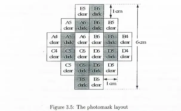
Finally the cells are arranged on the photomask according to Figure 3.5. As it is stated before, there are 3 layers on the mask. Layer 4 indicates the first mesa isolation, layer 5 indicates the second mesa isolation, and layer 6 the p-contact metalization. Cell A contains the small rings (Figure 3.4), cell B contains the big rings. Cells C and D contain the similar structures but with longer coupling distances of the radius of the rings. The dark and the clear cells are just image reversals of each other, which will be explained in the photolithography section.
Our mask file, which was prepared by the help of Wavemaker software, was sent to Compugraphics International Inc., Scotland, United Kingdom via e-mail. In three weeks the mask was ready for the fabrication.
3.2
Wafers and Sample Cleavage
After the mask is ready the laser diode fabrication begins with the form of a circular GaAs wafer 2 inch (5.08cm) in diameter and about 0.5mrn in
CHAPTER 3. DESIGN AND EABRICATION
29
800 micron diameter ring laser array 800 micron diameter ring laser array 800 micron diameter ring laser array 600 micron diameter ring laser array 600 micron diameter ring laser array 600 micron diameter ring laser array 400 micron diameter ring laser array 400 micron diameter ring laser array 400 micron diameter ring laser array
Figure 3.4: The organization of laser arrays
On the photomask the laser arrays are defined according to this pattern. Each process ends up with the fabrication of 400, 600, and 800/xm diameter ring lasers
E5 dear dnk i_ 1 cm r A5 dear ;'cferk4 B5 :<fedc; B5 dear AA dear ycfaiM A6 dear B6 dear B4 dear G4 dear v.iv« G5 dear D5 dear EX4 dear C5 dear y,E6·' D5 dear 'T is * daki B5 dear I c m 6cm
Figure 3.5: The photomask layout
CHAPTER 3. DESIGN AND FABRICATION
30
thickness (Figure 3.6). The wafers are cleaved into small pieces about 2cm^ area. The most important point is that the Fabry-Perot lines should be parallel to the primary fiat, which is the long straight line along the periphery of the wafer, and positioned originally to identify crystalline directions lying within the surface plane. There are two reasons for that. The first reason is the good wet etch profile in this direction. The second reason is the ease to cleave the sample perpendicular to the primary fiat, in order to obtain the cavity mirrors.
Figure 3.6: (100) p-type wafer convention
For (100) oriented wafers the primary flat is a (011) plane, and normal to this flat is defined by [0 1 1] direction
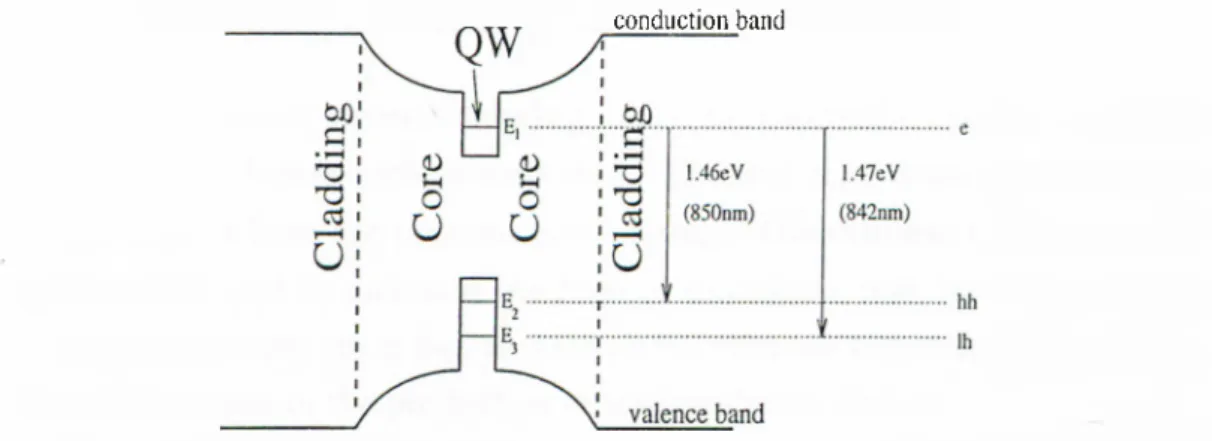
As it is also explained in the second chapter, when a very thin layer (on the order of a few tens of nm), e.g., of GaAs, is sandwiched between two higher band gap semiconductor materials, e.g.. Graded Index Separate Confinement Heterostructure (GRINSCH) AlGaAs, we obtain the quantum well (QW ) structure. This confinement leads to the development of a set of discrete energy levels in conduction and valence bands of QW layer as shown in Figure 3.7.
The position of these levels are a function of the thickness of the well layer as well as band offsets. This enables the control over the wavelength of the emitted photons due to the recombination of carriers. In addition to the carrier confinement in the quantum well, the surrounding layers, due to their lower refractive index, also provide a natural waveguide for photons generated in the QW region.
CHAPTER 3. DESIGN AND FABRICATION
31
conduction band
Figure 3.7: The band diagram and energy levels of the GRINSCH structure Our (lOO)p-type wafer labeled as ” B641” is an MBE (Molecular Beam Epitaxy) grown p-n junction with double GaAs quantum wells (DQW) embedded in AlGaAs cladding region. The layer structure, dopants, doping concentrations are shown in Figure 3.8. This wafer was grown by Glasgow University, EEE Department. m a tc h in g
core
core
matchinc ().15mic.5cl8Bc-GaA5 CAP1.2 mic. 5c 17 Bc-AlGaAs (x=0.4) CLADDING
0.03 mic. un-AlGaAs (x graded fmm 0.2 lo 0.4) MATCHING 0.1 mic. un-AlGaAs (x=0.2) CORE
QU3.ntUITl i^^Angstrom un-GaAs QUANTUM WELL
wells '
lOOAngstrom un-AIGaAs (x=0.2) BARRIER l(X)Angstromun-GaA.s QUANTUM WELL 0.1 mic. un-AIGaA.s (x=0.2) COREl e i 8 Si doped n-GaAs
substrate
0.03 mic. un-AlGaAs (x graded fmm 0.4 to 0.2) MATCHING
1.5 mic. 5c 17 Si-AIGaAs (x=0.4) CLADDING
0.5 mic, 5cI8 Si-GaA.s BARRIER
lcl8Si-GaA.s SUBSTRATE