TOPOLOGICAL VARIATIONS OF THE INVERSE DUAL CONVERTER FOR HIGH POWER DC-DC APPLICATIONS
M. Ehsani, L. Laskai and M.O. Bilgiq senior member, IEEE member, IEEE
Power Electronics Laboratory Dept. of Electrical Engineering
Texas A&M University College Station, T X 77843
Abstract- New dc to dc converter topologies are presented which are suitable for high density high power supplies. Topo- logical variations of the basic inverse dual converter (IDC) cir- cuit such as the transformer coupled, the multiphase and the multipulse derivation of the single phase IDC have been anal- ysed and some simulation results have been presented. It has been shown in a recent publication [l] that the single phase IDC offers a buck-boost operation over wide range without trans- former, bidirectional power flow, and complementary commuta- tion of the switches.
The topologies examined in this paper have additional features such as lower device and component stresses, and smaller filter requirements, resulting in smaller size and weight. Some performance and possible applications are also examined. Finally the IDCs for serial and parallel power distribution, and ac tapping of the IDC are discussed.
Introduction
High power dc to dc conversion has been receiving an in- creasing interest in the past years as the result of increased de- mand for high power converters in aerospace, defence and terres- trial applications. At the present time a wide selection of switch mode topologies, based on pulse width modulated (PWM) or resonant power processing, are available for implementation at lower power levels, up to several hundred Watts. However the medium and especially high power end of dc to dc converters have received less attention. One technique commonly used for higher power levels has been the full bridge topology operated with PWM control strategy. This topology offers a minimal voltage stress on the devices, and a low ripple current in the input and output capacitors. By increasing the switching fre- quency, the size and the weight of the reactive components are reduced. However the frequency achievable is limited by switch- ing losses, transformer leakage inductance and output rectifier reverse recovery time. These factors constrain the maximum frequency, component size, and thus the power density achiev- able. Higher power densities have been achieved by operating full bridge topology in resonant mode. The reason for this being
that high power converters are still dominated by SCRs, and the most efficient way to reduce the switching loss is by terminating the conduction of the thyristors by placing them in resonant cir- cuits. Power density of lkW/kg has been reported with series resonant converters (SRC) at 10kHz. Converters of this type have been fabricated with power capabilities in the order of 100 kW [2]. But, the resonant operation also has its penalties such as frequency sensitivity, and higher voltage and current stress in the devices.
The dual active bridge converter has been proposed for high power dc to dc conversion in [4]. This voltage driven dc to dc converter consists of two inverting stages operating at a high frequency with controlled phase shift. This topology utilizes the leakage impedanceof the coupling transformer as the energy transfer element. However, at high frequencies and high power levels the realization of the transformers with controlled leakage inductance is a challenging task. The soft switching control strategy proposed imposes severe limitations on the load range and allowed input voltage variations, in order to maintain soft switching on all the switches.
Fig.1 Single-phase IDC
A voltage source derivation of the inductor converter bridge (ICB) circuit [3], the inverse dual converter (IDC), shown in Figure 1, has been proposed in [l]. The dual active bridge con- verter proposed in [4] represents the dual of IDC. By suitable control the IDC topology provides buck-boost operation, with- out a transformer, and is capable of bidirectional power flow. In most applications where the load is a motor, isolation between motor load and dc bus is not necessary, because motor itself pro-
vides the electrical isolation that may be required in converters for safety or other reasons
.
For applications where dc isolation is required an ac link transformer can provide the necessary isolation. Since capacitive energy storage is much better than inductive energy storage in terms of per unit size and weight, capacitive energy transfer used in IDC is an important advan- tage to improve power density["I.
The ac link capacitor also provides the necessary commutation voltage across the switch- ing devices, allowing the use of SCRs, at frequencies in excess of 20 kHz, without additional commutating circuits. Therefore, the power rating of the IDC can be scaled up to MW levels us- ing well known high power SCR bridge technology. In most of the expected high power applications the use of SCR switches is a reliable and economical solution. However, in order to in- crease the operating frequency beyond 20 kHz devices such as MOS-controlled thyristors [SI, IGBTs or G.T.O. thyristors (61 have to be considered. The combination of gate turn off and available commutation voltage will offer efficient switching at higher frequency and zero current.The detailed analysis of the single phase IDC is given in [l]. A short review of the analysis is given as an introduction for the more sophisticated members of the IDC family.
7
T h e Basic IDC
't
The operating waweforms of the single phase IDC with the load side bridge control angle leading ( power transfer from source to the load ) are shown in Figure 2. The switching sequelice on the source side bridge is ssl ss4, ss2Ss3, sslss4 etc. and the same switching pattern is used on the load side. It has been shown that the average load power in a lossless single phase IDC converter isISIL
d2
w c a
<
P>=
-(4--)
0<
4 < awhere Is and I L are the average inductor currents, w is the angular frequency of the converter,
4
is the load side bridge advance angle and C is the link capacitor.",
1'
Fig.2 Waveforms associated with single-phase IDC; ac link capacitor voltage U = , input and output choke voltage v, and 01
By applying gyrator theory the dc gain has been found as
w c
VO
< -
>=
K
4-(o"/.)R
where R represents the load resistance. The gain formula shows that the control of the IDC can be achieved by adjusting the phase and the frequency, or both. Both voltage step-up and step-down is possible continuously through a wide range without a need for a transformer. Various control strategies could be implemented, such as regulated output control, tracking output voltage control, constant output current control, constant load power control or constant input power. These strategies are application dependent and they subject of further research.
It has been shown in [l], that the single- phase IDC possesses several attractive features, such as
a) buck-boost operation, b) bidirectional power processing, c)
d) simple circdt impiementation, e) s m hl number of components, f ) efficient high frequency operation, g) unlimited high power capability.
To further increase the power density, that is to decrease the component sizes, and decrease the device and component stresses in different applications, variations of the basic IDC are appropriate as described in this paper.
capacitive commutation of the switches,
M u l t i p h a s e IDC
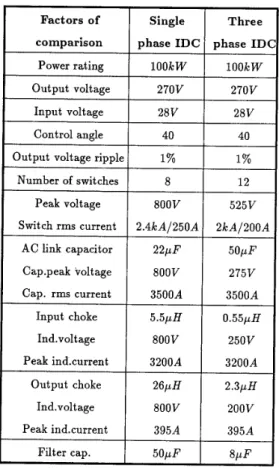
One way to produce a low input current ripple and output voltage ripple is the multiphase IDC. Figure 3 shows the three phase IDC. In exchange for additional switches the device and component stresses have been decreased ( Table 1 ), and the input and output filtering requirements are substantially lower when compared to single phase IDC. The converter in Figure 3 consists of two phase shifted, capacitor coupled, three phase inverter stages operating at a high frequency in six-step mode
Fig.3 Three-phase IDC
The average power transferred from left to right for a lossless converter is
<
P>
= -(24-ISIL
-) 3d2 f O T 0 < 4 < ? 3 w c 2a I ~ I L 3d2 a 27r w c ~6 3 3<
P>
= -(34 - - - -) fOT -<
4
<
-
(3) I S I L 342 A 2% w c 27r 2 3 < p > = - ( 4 - - + - ) f O T- < d < / .
1263Factors of comparison Power rating Output voltage Input voltage Control angle Output voltage ripple
Number of switches Peak voltage Switch rms current AC link capacitor Cappeak voltage Cap. rms current Single Three
phase IDC phase ID lOOkW lOOkW 270V 270V 28V 28V 40 40 1% 1% 8 12 800V 525V 2 . 4 k A / 2 5 0 A 2 k A / 2 0 0 / 2 2 p F 5 0 p F 800V 275V 3500A 3500A
TABLE I. The comparison of single-phase IDC and three-phase IDC
Input choke 1nd.volt age Peak ind.current Output choke 1nd.voltage Filter cap. Peak ind.current
The gam of the three-phase IDC is given by
5 . 5 p H 0 . 5 5 p H 800V 250V 3200A 3200A 26pH 2 . 3 p H 800V 2 0 0 v 3 9 5 8 3 9 5 4 5 0 p F 8 P F wCR
< - > =
VO f O T 0 < 4 < :Vi
2 4 - ( 3 4 ’ / 2 l ~ ) w C R 27 3 f O T - < 4 < K VO Vi< - > =
4
- ( 3 4 ’ / 2 ~ )+
( ~ / 2 )It can be shown from Eqn.(2) and Eqn.(4) that the ac link capacitor required per phase for the three-phase topology is twice the value of that required for the single -phase IDC of the same power. But since the current and voltage of the capacitor has been decreased the size and weight of these capacitors is smaller. By maintaining the same ripple current through the source and load inductors, the inductors will be approximately an order of magnitude smaller than in the single- phase counterpart. The peak voltage across the switches is decreased six times. Overall, for the same power level the three phase IDC is significantly smaller than the single-phase IDC. A comparison between these converters has been shown in Table 1 for boost operation. Furthermore the reliability of the converter has been increased since in case of a switch failure the three-phase converter can make a transition to a single-phase operation by providing the appropriate means of control.
The Transformer Coupled IDC
In order to achieve dc isolation and lower device stresses the transformer coupled IDC can be implemented. This config- uration, shown on Figure 4a, will reduce the rating of the input bridge converter switches. Since the ac voltage rating of the capacitors at high frequencies is a critical factor this topology provides the benefit of voltage rating reduction of the link ca-
lbl
Fig.4 (a) Transformer coupled IDC
(b) IDC with integrated transmission line
The parallel distribution of IDC bridges for two loads is shown in Figure 6. Both topologies are capable of supporting individually regulated buck-boost operation for isolated loads. Regenerating loads can augment the source converter in supplying the other load. Furthermore, the source and loads could be placed in pacitor for the same output voltage. The design of this converter requires additional attention in order to avoid possible undesir- able resonant effect between the ac link capacitor and magne- tizing inductance of the transformer. The transformer coupled concept is naturally expandable to an ac power transmission line linking the source and the load ( Figure 4b ). The trans- mission voltage magnitude can be as high as required, indepen- dently of the input voltage, furthermore, the voltage magnitude and phase can be controlled to accommodate system operational constraints. Although it provides some advantages, integration of the transmission line into the IDC design does not necessitate a transformer.
’
Power Distribution Topologies
For high power applications where several dc loads are served, and output regulation is required two topologies are examined. The serialiy connected IDC’s for two loads is shown in Figure 5 , where the individual bridges could be single or multi phase, suitable for a converter with multiple regulated outputs. 1264
The parallel distribution of IDC bridges for two loads is shown in Figure 6. Both topologies are capable of supporting individually regulated buck-boost operation for isolated loads. Regenerating loads can augment the source converter in supplying the other load. Furthermore, the source and loads could be placed in
phase variation
4
for lower values of the operating angle. When the angle control enters the sensitive range frequency control provides new operating limits for phase control with desired sensitivity and gain. This can be derived also from the Eqn.(2) by solving the equation for phase4,
Fig.5 Serially connected IDCs
different sites, by providing a high frequency ac transmission line between them. The advantages of high frequency ac power distribution from the standpoint of reduced size and weight of magnetic components and with regard to filtering requirements
1 7
This equation shows that if we want to operate at higher loads which are maybe beyond the phase control region the frequency could be changed in order to get a stable operating point.
Furthermore, substantial input ripple current reduction can be achieved by controlling the upper bridge phase angle in respect to the lower bridge switching pattern when both bridges operates at same frequency.
Fig.8 AC tapping of the IDC
For applications where ac and dc loads are present the scheme shown on Figure 8 will be optimal. Simulation results have shown that ac link can be loaded to more than 50% of the overall converter rating and still allow regular operation of the converter. When both frequency and phase are used to control the dc gain then the tapped ac resistive load is
However, if only the phase is varied in order to adjust the
the penalty of limited operating range. Fig.6 IDCs connected in parallel
are established [81. the parallel distnbutlon scheme the serially connected IDC provides a fully independent control of the individual converters. Both phase and frequency control
using phase and frequency control at the same time is elaborated in following. The gain curve of a single phase IDC is shown in Figure 7. As seen from this figure, the gain is very sensitive to
strategies can be to each ID'. The advantage Of frequency control may be applied to control the ac voltage with
GA'::L
PHASE ANGLE,
Fig.7 Gain curve
Conclusion
Several topological variations of the inverse dual converter have been presented for high power applications. These topolo- gies have most of the IDC features such as buck-boost opera- tion, bidirectional power processing, capacitive commutation for switches, and unlimited high power capability.
The multiphase, the transformer coupled and the power distribution IDC topologies offer some additional properties such as significant power density improvement, isolation, ac tapping, and input current reduction.
A quantitative comparison between the single and the multiphase IDC has been also presented.
Acknowledgment
We would like to gratefully acknowledge the support of General Dynamics, Fortworth Division and Center for Space Power at Texas A&M College of Engineering.
Jayanthi Arvind for her simulation assistance in this work.
We are also indebted t o Ms.
REFERENCES
[l] M. Ehsani, I. Husain and M.O. Bilgic, “Inverse Dual Con- verter (IDC) for High Power DC-DC Applications”, IEEE- PESC Conf. Rec., 1990.
F.C. Schwarz and J.B. Klassens, “A Controllable 45-kW Current Source for DC Machines”, IEEE Trans. on Ind.
M. Ehsani, R.L. Kustom and R.W. Boom, “One-phase Dual Converter for Two-Quadrant Power Control of Supercon- ductive Magnets”, IEEE Trans. on Magnetics, Vol. MAG- 21, No. 2, March 1985.
[2]
Appl., Vol. IA-15, NO. 4, pp. 437-444, J d . / Aug. 1979. [3]
[4] R.W. De Doncker, D.M. Divan and M. Kheraluwala, “A Three-phase Soft-switched High Power Density DC-DC Converter for High Power Applications”, IEEE
-
IAS Conf. Rec., pp. 796-805, 1988.T.M. Jahns, R.W. Doncker, J.W.A. Wilson,V.A.K. Temple and D.L. Watrous, “Circuit Utilization Characteristics of MOS-controlled Thyristors”, IEEE - IAS Conf. Rec., pp. 1248-1254, 1989.
R.J. Morris, F.J. Wakeman, L. Malesani, L. Rossetto and P. Tenti, “A New Family of G.T.O. Devices for Medium Frequency Applications”, IEEE-IAS Conf. Rec., pp. 1264- 1269, 1989.
S. Cuk and R.D. Middlebrook, “A New Optimum Topology Switching DC-to-DC Converter”, IEEE - PESC Conf. Rec., 1977.
0. Wasynczuk and P.C. Krause, “Simulation and Control of a 20-kHz Spacecraft Power System”, IEEE Trans. on Aerospace and El. Sys., Vol. 25, No. 5, pp. 668-675, Sept. 1989. [5] [6] [7] [8] 1266