Realistic Channel Temperature Simulation of
AlGaN/GaN High Electron Mobility Transistors
Oğuz Odabaşı
#*
1, Bayram Bütün*
2, Ekmel Özbay
#*
3#Nanotechnology Research Center (NANOTAM), Bilkent University, Ankara, Turkey
*Department of Electrical and Electronics Engineering, Bilkent University, Ankara, Turkey
1[email protected], {2bbtn, 3ozbay}@bilkent.edu.tr
Abstract — In this work, the realistic channel temperature of AlGaN/GaN High Electron Mobility Transistors (HEMTs) is investigated by using 2D electrothermal and Finite Element Method (FEM) thermal simulations. By using a special method to map the position dependent heating in a device, more accurate results in channel temperature are achieved compared to the conventional FEM methods. With this method, larger device areas can be simulated more accurately with less complexity.
Keywords — AlGaN/GaN, High-Electron-Mobility-Transistors (HEMT), reliability, semiconductor device thermal factors
I. INTRODUCTION
AlGaN/GaN HEMTs are promising candidates for high power applications [1]. They can work under high voltage and current thanks to the wide band gap of GaN [2,3]. High electron mobility and concentration are achieved with the high bandgap difference between AlGaN and GaN and polarization fields [4]. However, this technology suffers from self-heating and current collapse effects [5]. Self-heating is the increase of the device temperature while conducting current. The mobility, electron velocity and channel charge density are temperature dependent and, therefore, an increase in the channel temperature affects the device performance directly [6]. In addition, the capture and emission processes of traps are temperature dependent. The temperature change of the device effectively alters trap behavior and needs to be known precisely [7]. Therefore, the information of the correct temperature of the device becomes crucial in simulating and optimizing device performance.
In the determination of the channel temperature of AlGaN/GaN devices, several measurement and simulation methods are used. Micro-Raman measurement [8], infrared camera [9], visible-UV spectroscopy [10], and electrical measurements [11] are the most common methods. In addition, trap activation energy calibration is used in the literature [12]. All of these methods have advantages as well as limitations [13]. Micro-Raman measurement can reach submicron spatial resolution but requires a direct optical path to the measurement point. Therefore, this method is not useful for devices that have field plates and T-gate structures. An infrared camera is easy to use, but the spatial resolution of this method is larger than the whole active region of some transistors and, therefore, the results are imprecise. Electrical measurements are easy to perform and do not require expensive equipment to implement
because basic laboratory equipment is enough for this method. The results yield the average temperature of the channel because the information is derived from the current, which is misleading in the correct calculation of the maximum temperature of the channel [14]. These factors led researchers to use electrothermal and finite element method-based simulations as complementary tools [9,15,16,17]. These simulations provide information about the internal dynamics of devices and help the optimization process by reducing iterative trials in fabrication. However, there is also a trade-off between the precision, time, and processing requirements. In electrothermal simulations, Poisson, diffusion and thermal equations are solved iteratively for each distributed point in a device. Therefore, large device areas are not preferred due to the computational load. FEM simulations are good candidates for simulating devices in real dimensions, but the precision of simulations is lower than electrothermal simulations.
A novel method is proposed in this paper in order to combine the accuracy of the electrothermal simulations and simulation area of FEM simulations. The results are compared with the conventional methods used in FEM simulations and better accuracy is achieved in the correct determination of channel temperature. In section Ⅱ, the details of electrothermal simulation and the heat map forming method are discussed. In section Ⅲ, FEM simulation details and the implementation of the heat map are explained. In Section Ⅳ, the proposed method is compared with the conventional methods used in FEM simulations. In the conclusion section, the obtained results are summarized, and future work is explained.
II. ELECTROTHERMAL SIMULATION
A conventional AlGaN/GaN device structure is proposed to be electrothermally simulated in 2D in commercial simulation tool Silvaco/ATLAS, which solves Poisson's equations,
𝛻(𝜀𝛻𝜑) = −𝑞(𝑝 − 𝑛 + 𝑁𝐷− 𝑁𝐴) − ρ𝑡𝑟𝑎𝑝 (1)
current continuity equations, 𝛻𝐽⃗⃗⃗ = 𝑞𝑅𝑛 𝑛𝑒𝑡 + 𝑞 𝜕𝑛 𝜕𝑡 (2) −𝛻𝐽⃗⃗⃗ = 𝑞𝑅𝑃 𝑛𝑒𝑡 + 𝑞 𝜕𝑝 𝜕𝑡 (3)
Proceedings of the 1st European Microwave Conference in Central Europe
and thermal equation simultaneously, 𝑇̃ = 𝑅𝑡ℎ𝑃 + 𝑇0 (4)
where 𝜑 is the electric potential, p and n are the hole and electron, 𝑁𝐷and 𝑁𝐴 are the donor and acceptor concentrations,
respectively. ρ𝑡𝑟𝑎𝑝 represents the trap density and 𝑅𝑛𝑒𝑡 is the
net recombination-generation rate [18]. 𝑇̃ is the channel and 𝑇0
is the base temperature. 𝑅𝑡ℎ and 𝑃 symbolize the thermal
resistance and the dissipated power.
Simulated device structure and important dimensions are provided in Fig. 1.
Fig. 1: The Schematic of the Device Structure
Material parameters are defined as temperature dependent in order to get the most realistic results. The III-Nitride specified mobility model is used for AlGaN and GaN, based on the fitting of Monte-Carlo simulation results [19]. Isothermal boundary condition of 300K is applied at the bottom of the device as a heat sink, and the other boundaries are defined as adiabatic (𝜕𝑇𝜕𝑥= 0). Mesh points are assigned by considering the rate of change of the electric field and charge density.
The total generated heat power density (W/cm3) is
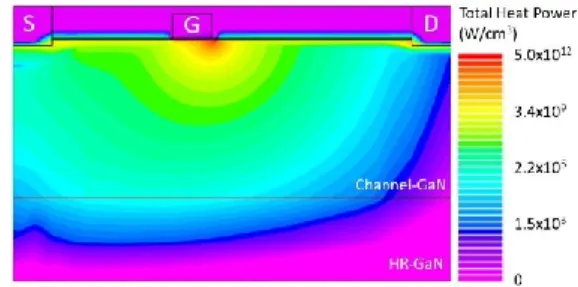
calculated at every mesh point for a different gate and drain bias conditions. It is seen in Fig. 2 that when current starts to conduct in the channel, as a result of the Joule heating, energy is dissipated in the channel, which is denser under the drain side of the gate contact. As it moves away from the channel, the generated heat power density decreases with the decrease in the current density.
Fig. 2: Total Generated Heat Power at Vgs = 0V Vds = 10V Bias
The reason for this localization of heat generation at the drain side corner of the gate is the strong electric field in the channel below the drain side of the corner of the gate. Charge accumulation occurs at the drain side of the gate because of the applied drain voltage. This field causes high electric field, more depletion of the 2DEG and causes the reduction of conductivity [20]. In order to understand this behavior of conductivity along
channel in a better way, it is plotted for gate voltages from -6 V to 2 V in the Fig. 3 (a). When the gate voltage is less than pinch-off voltage, the conductivity under the gate is nearly zero because the gate is closed and the 2DEG under the gate is fully depleted. Because there is no current passing through the channel, the Joule heating is negligible so the temperature of the channel is the same with the heat sink. In order to understand the effect of heating on conductivity, in Fig. 3(b) the conductivity is calculated by neglecting the self-heating effect in simulations. For every gate voltage, the conductivity is the same in the channel except the gate, which shows that the reason for the decrease of the conductivity along the channel is the temperature increase because of the Joule heating.
(a)
(b)
Fig. 3: Conductivity along the channel (a) with (b) and without self-heating
When the applied gate bias is more than pinch-off voltage, the channel opens and starts to conduct current. Because of high electric field and high temperature, conductivity dips under the drain side of the gate contact [21], which causes denser heat generation.
The generated heat power data at every mesh point is stored by using the PROBE method in a file generated by Silvaco/ATLAS. This data is extracted by using MATLAB. A heat map is formed by considering the positions of each mesh point and their stored generated heat information. Through this method, we applied a heat generation map to COMSOL as a position dependent look up table. The conductivity map can be used with the relationship explained hereinabove. The position dependent conductivity can be implemented in COMSOL and the generated heat can be calculated by the Joule heating module.
III. FEMSIMULATION
The COMSOL Finite Element Analysis Tool [22] is used for thermal 2D FEM analysis in this work. This software enables us to enter a position dependent heat source and calculate the temperature of the structure with proper boundary conditions and material properties. It divides the structure into
meshing shapes and calculates the desired properties for these small pieces. The same structure with Silvaco/ATLAS is simulated in COMSOL. In order to increase the consistency between two simulations, the same geometric parameters and boundary conditions are used. A constant temperature of 300K is assigned to the bottom of the device and other boundary conditions are defined as adiabatic.
One of the main causes of mismatch between simulations with different approaches is the non-standard material properties with large deviations. In the default material properties of the COMSOL and ATLAS, there are differences. As an example, the thermal conductivity of GaN used in both simulations and from a widely used and referred work [16] is plotted in Fig. 4. Large mismatch over a wide temperature range can be seen. In this work, the material models used in ATLAS are implemented to the COMSOL to get the best fitting between simulations.
Fig. 4: Thermal conductivity of GaN different sources with respect to temperature
Another important parameter of simulation which affects the reliability of the results is the mesh number and size. If the mesh number is not enough, the fast changes cannot be processed, and the results become incorrect. Therefore, finer meshing is used for the areas wherein fast changes occur (i.e. electric field, electric potential, charge concentration). We tested the reliability of our meshes as the stability of results under the increasing mesh density.
IV. RESULTS AND DISCUSSION
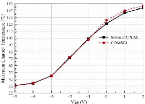
The same structure is simulated both in Silvaco/ATLAS and COMSOL. The total generated heat density map is extracted from electrothermal simulations and implemented in the FEM simulation as a position dependent heat source with a look up table. The heat power density value for intermediate positions is derived by the linear interpolation of the lookup table. We observed perfect matching between simulations. Fig. 5 shows the maximum temperature values simulated in both programs. The maximum error observed is 3°C when the gate voltage is 2 V, which corresponds to a nearly 2.5% temperature increase.
After calibrating the simulations, we investigated the accuracy of the conventional methods used in FEM simulations to model the heating of the AlGaN/GaN HEMTs. In many works [16,17,23], the generated heat power is distributed evenly over the surface between gate and the AlGaN in order to reduce the complexity and simulate larger device areas. The same assumption is followed in order to make a comparison. We implemented exactly the same amount of heat generation
rate for both models and observed the maximum temperature simulated in the device as well as the temperature distribution.
Fig. 5: Maximum temperatures simulated in COMSOL and Silvaco ATLAS with respect to gate bias
In Fig. 6, the simulated channel temperatures by using the proposed method of heat map and the conventional method of uniform heat source under the gate contact are plotted along the channel.
Fig 6: Comparison of simulated channel temperatures
The proposed method of heat map implementation successfully exhibits the temperature behavior observed in electrothermal simulations. At the drain side of the gate, the temperature makes a peak of 140°C and decreases through the source and drain contacts slows. The uniform heat source over-estimates the temperature under the gate with peak temperature of 170°C and underestimates the temperature along the channel. In this method, all of the generated heat is assumed to be placed under the gate, but according to electrothermal simulations, especially for high channel currents, the heat generated at the channel becomes comparable with the heat generated under the gate. The proposed method includes the heat generation in the channel at the right position, so the channel temperature and maximum temperature are correctly simulated. In addition, a uniform heat source cannot give information about the hot spot. It is symmetrical along the gate and results a parabolic temperature under the gate that peaks at the center of the gate.
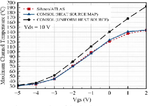
The maximum simulated temperatures for both methods for gate voltages from -5 V to 2 V with a drain voltage of 10 V are plotted in Fig. 7, and the maximum temperature values and errors with respect to Silvaco/ATLAS 2D electrothermal simulation are provided in Table 1. As the electric current along channel increases, the Joule heating in the channel becomes more dominant and the difference between the simulated temperatures of electrothermal simulation and uniform heat source in FEM increases. However, in the proposed method, the
error stays below 3% and shows a good match with the electrothermal simulation.
Fig. 7: Comparison of simulated temperatures
Table 1: Simulated temperatures and corresponding errors with respect to Silvaco simulation Gate Voltage (V) Silvaco Max. Temp. (°C) HM(i) Max. Temp. (°C) HM Error (°C) UHS (ii) Max. Temp. (°C) UHS Error (°C) -5 31 30.8 0.2 32.1 1.1 -4 34 34.8 0.8 36.6 2.6 -3 45 44.9 0.1 49.9 4.9 -2 71 72.5 1.5 80.7 9.7 -1 99 97.3 1.7 113 14 0 121 126 5 142 21 1 137 140 3 170 33 2 144 147 3 195 51
(i) Heat Map (Extracted from Silvaco/ATLAS) (ii) Uniform Heat Source (Applied Under Gate Contact)
V. CONCLUSION
In this work, we have used 2D electrothermal simulations to create a position dependent generated heat power density map to be used in finite element method simulations. We have calibrated two simulations by simulating the same structures and thereby resulting in the same temperature distributions. Then, proposed method has been compared with the conventional method of defining a uniform heat source at the gate-AlGaN interface by implementing both methods on the same structure. We observed that our proposed method successfully exhibits convenient results with electrothermal simulations, whereas the conventional method overestimates the temperature under the gate and underestimates the temperature along the channel. Thanks to the proposed method, larger areas of the devices can be simulated with higher precision and fewer computational requirements. This is important in device design for optimization and reliability measurements to obtain the correct temperature. Thermal camera and electrical measurements on real devices are in progress. In order to overcome the measurement and simulation limitations, we are planning to combine and match them by implementing filters in thermal simulations for infrared camera measurements as well as pulsed and electrical measurements with transient analysis.
REFERENCES
[1] R. J. Trew, “SiC and GaN transistors - Is there one winner for microwave power applications?” Proc. IEEE, vol. 90, no. 6, pp. 1032–1047, 2002. [2] U. K. Mishra, P. Parikh, and Y. F. Wu, “AlGaN/GaN HEMTs - An overview of device operation and applications,” Proc. IEEE, vol. 90, no. 6, pp. 1022–1031, 2002.
[3] U. K. Mishra, L. Shen, T. E. Kazior and Y. Wu, "GaN-Based RF Power Devices and Amplifiers," in Proceedings of the IEEE, vol. 96, no. 2, pp. 287-305, Feb. 2008.
[4] Y. Zhang and J. Singh, “Charge control and mobility studies for an AlGaN/GaN high electron mobility transistor,” J. Appl. Phys., vol. 85, no. 1, pp. 587–594, 1999.
[5] R. Gaska, A. Osinsky, J. W. Yang and M. S. Shur, "Self-heating in high-power AlGaN-GaN HFETs," in IEEE Electron Device Letters, vol. 19, no. 3, pp. 89-91, March 1998.
[6]J. W. Lee and K. J. Webb, “A temperature-dependent nonlinear analytic model for AlGaN-GaN HEMTs on SiC,” IEEE Trans. Microw. Theory Tech., vol. 52, no. 1 I, pp. 2–9, 2004.
[7] O. Mitrofanov and M. Manfra, “Mechanisms of gate lag in GaN/AlGaN/GaN high electron mobility transistors,” Superlattices Microstruct., vol. 34, no. 1–2, pp. 33–53, 2003
[
8] M. Kuball and J. W. Pomeroy, “A review of raman thermography for electronic and opto-electronic device measurement with submicron spatial and nanosecond temporal resolution,” IEEE Trans. Device Mater. Reliab., vol. 16, no. 4, pp. 667–684, 2016.[9] A. Sarua, M. Kuball, M. J. Uren, T. Martin, K. P. Hilton, and R. S. Balmer, “Integrated micro-Raman/infrared thermography probe for monitoring of self-heating in AlGaN/GaN transistor structures,” IEEE Trans. Electron Devices, vol. 53, no. 10, pp. 2438–2447, 2006.
[10] I. Ahmad, V. Kasisomayajula, D. Y. Song, L. Tian, J. M. Berg, and M. Holtz, “Self-heating in a GaN based heterostructure field effect transistor: Ultraviolet and visible Raman measurements and simulations,” J. Appl. Phys., vol. 100, no. 11, 2006.
[11] J. Kuzmík, P. Javorka, A. Alam, M. Marso, M. Heuken, and P. Kordoš, “Determination of channel temperature in AlGaN/GaN HEMTs grown on sapphire and silicon substrates using DC characterization method,” IEEE Trans. Electron Devices, vol. 49, no. 8, pp. 1496–1498, 2002.
[12] F. Soci, A. Chini, G. Meneghesso, M. Meneghini, and E. Zanoni, “Influence of device self-heating on trap activation energy extraction,” IEEE Int. Reliab. Phys. Symp. Proc., p. 3C.6.1-3C.6.6, 2013.
[13] N. Killat, M. Kuball, T. M. Chou, U. Chowdhury, and J. Jimenez, “Temperature assessment of AlGaN/GaN HEMTs: A comparative study by Raman, electrical and IR thermography,” IEEE Int. Reliab. Phys. Symp. Proc., pp. 528–531, 2010.
[14] S. P. McAlister, J. A. Bardwell, S. Haffouz, and H. Tang, “Self-heating and the temperature dependence of the dc characteristics of GaN
heterostructure field effect transistors,” J Vac Sci Tech A, vol. 24, no. 3, pp. 624–628, 2006.
[15] T. Yonemura, M. Furukawa, S. Mizuno, S. Matsukawa, M. Shiozaki, and Y. Namikawa, “High-Accuracy Product Life Estimation of GaN-HEMT by µ – Raman and Numerical Simulation,” no. 86, pp. 125–130, 2018. [16] F. Bertoluzza, N. Delmonte, and R. Menozzi, “Three-dimensional finite-element thermal simulation of GaN-based HEMTs,” Microelectron. Reliab., vol. 49, no. 5, pp. 468–473, 2009.
[17] X. Chen, W. Zhai, J. Zhang, R. Bu, H. Wang, and X. Hou, “FEM thermal analysis of high power GaN-on-diamond HEMTs,” J. Semicond., vol. 39, no. 10, p. 104005, 2018.
[18] Device Simulation Software, ATLAS User’s Manual, Silvaco Int., Santa Clara, CA, 2009
[19] M. Farahmand et al., “Monte Carlo Simulation of Electron Transport in the III-Nitride.pdf,” vol. 48, no. 3, pp. 535–542, 2001.
[20] H. Morkoç, Nitride Semiconductor Devices: Principles and Simulation Properties of Group-IV , III-V and II-VI Semiconductors Nitride
Semiconductors. 2008.
[21] X. D. Wang, W. Da Hu, X. S. Chen, and W. Lu, “The study of self-heating and hot-electron effects for AlGaN/GaN double-channel HEMTs,” IEEE Trans. Electron Devices, vol. 59, no. 5, pp. 1393–1401, 2012. [22] COMSOL Multiphysics 3.5a User’s Guide, COMSOL AB, 2008 [23] R. Menozzi et al., “Temperature-Dependent Characterization of AlGaN/GaN HEMTs: Thermal and Source/Drain Resistances,” IEEE Trans. Device Mater. Reliab., vol. 8, no. 2, pp. 255–264, 2008.