Localized plasmon-engineered
spontaneous emission of CdSe/ZnS nanocrystals
closely-packed in the proximity of
Ag nanoisland films for controlling
emission linewidth, peak, and intensity
Ibrahim Murat Soganci, Sedat Nizamoglu, Evren Mutlugun, Onur Akin, and Hilmi Volkan Demir
Department of Physics, Department of Electrical and Electronics Engineering, Nanotechnology Research Center, Bilkent University, Ankara, 06800 Turkey
Abstract: Using metallic nanoislands, we demonstrate the localized
plasmonic control and modification of the spontaneous emission from closely-packed nanocrystal emitters, leading to significant changes in their collective emission characteristics tuned spectrally and spatially by plasmon coupling. Using randomly-distributed silver nanoislands, we show that the emission linewidth of proximal CdSe/ZnS core-shell quantum dots is reduced by 22% and their peak emission wavelength is shifted by 14nm, while their ensemble photoluminescence is enhanced via radiative energy transfer by 21.6 and 15.1 times compared to the control groups of CdSe/ZnS nanocrystals with identical nano-silver but no dielectric spacer and the same nanocrystals alone, respectively.
©2007 Optical Society of America
OCIS codes: (240.6680) Surface plasmons; (250.5230) Photoluminescence; (310.6860) Thin
films, optical properties; (310.1860) Thin films, deposition and fabrication; (260.3910) Metals, optics of; (160.2540) Fluorescent and luminescent materials; semiconductor nanocrystals, quantum dots.
References and links
1. V. I. Klimov, A. A. Mikhailovsky, Su Xu, A. Malko, J. A. Hollingsworth, C. A. Leatherdale, H.-J. Eisler, and M. G. Bawendi, “Optical gain and stimulated emission in nanocrystal quantum dots,” Science 290, 314-317 (2000).
2. D. Alexson, H. Chen, M. Cho, M. Dutta, Y. Li, P. Shi, A. Raichura, D. Ramadurai, S. Parikh, M. A. Stroscio, and M. Vasudev, “Semiconductor nanostructures in biological applications,” J. Phys.: Condens. Mat. 17, R637-R656 (2005).
3. S. Nizamoglu, T. Ozel, E. Sari, and H. V. Demir, “White light generation using CdSe/ZnS core-shell nanocrystals hybridized with InGaN/GaN light emitting diodes,” Nanotechnology 18, 065709 (2007). 4. R. Osovsky, V. Kloper, J. Kolny-Olesiak, A. Sashchiuk, and E. Lifshitz, “Optical properties of CdTe
nanocrystal quantum dots, grown in the presence of Cd0 nanoparticles,” J. Phys. Chem. C 111, 10841-10847
(2007).
5. A. A. Chistyakov, I. L. Martynov, K. E. Mochalov, V. A. Oleinikov, S. V. Sizova, E. A. Ustinovich, and K. V. Zakharchenko, “Interaction of CdSe/ZnS core-shell semiconductor nanocrystals in solid thin films,” Laser Phys. 16, No. 12, 1625-1632 (2006).
6. P. P. Pompa, L. Martiradonna, A. Della Torre, F. Della Sala, L. Manna, M. De Vittorio, F. Calabi, R. Cingolani, and R. Rinaldi, “Metal-enhanced fluorescence of colloidal nanocrystals with nanoscale control,” Nature Nanotechnology 1, 126-130 (2006).
7. J-H. Song, T. Atay, S. Shi, H. Urabe, and A. V. Nurmikko, “Large enhancement of fluorescence efficiency from CdSe/ZnS quantum dots induced by resonant coupling to spatially controlled surface plasmons,” Nano Lett. 5, No. 8, 1557-1561 (2005).
8. K. Okamoto, S. Vyawahare, and A. Scherer, “Surface-plasmon enhanced bright emission from CdSe quantum dot-nanocrystals,” J. Opt. Soc. Am. B. 23, No. 8, 1674-1678 (2006).
9. O. Kulakovich, N. Strekal, A. Yaroshevich, S. Maskevich, S. Gaponenko, I. Nabiev, U. Woggon, and M. Artemyev, “Enhanced luminescence of CdSe quantum dots on gold colloids,” Nano Lett. 2, No. 12, 1449-1452 (2002).
10. K. Ray, R. Badugu, and J. R. Lakowicz, “Metal-enhanced fluorescence from CdTe nanocrystals: a single-molecule fluorescence study,” J. Am. Chem. Soc. 128, 8998-8999 (2006).
11. I. Gryczynski, J. Malicka, W. Jiang, H. Fischer, W. C. W. Chan, Z. Gryczynski, W. Grudzinski, and J. R. Lakowicz, “Surface-plasmon-coupled emission of quantum dots,” J. Phys. Chem. B. 109, 1088-1093 (2005). 12. K. T. Shimizu, W. K. Woo, B. R. Fisher, H. J. Eisler, and M. G. Bawendi, “Surface-enhanced emission from
single semiconductor nanocrystals,” Phys. Rev. Lett. 89, No. 11, 117401 (2002).
13. J. R. Lakowicz, “Radiative decay engineering: biophysical and biomedical applications,” Anal. Biochem.
298, 1-24 (2001).
14. M. Kawasaki and S. Mine, “Highly efficient surface-enhanced fluorescence on Ag island film of large pseudotabular nanoparticles,” Chem. Lett. 34, No. 7, 1038-1039 (2005).
15. V. L. Schlegel and T. M. Cotton, “Silver-island films as substrates for enhanced Raman scattering: effect of deposition rate on intensity,” Anal. Chem. 63, 241-247 (1991).
16. K. Sonnichsen, Plasmons in metal nanostructures (Ludwig-Maximilians-University of Munich, 2001). 17. T. Nakamura and S. Hayashi, “Enhancement of dye fluorescence by gold nanoparticles: Analysis of particle
size dependence,” Jpn. J. Appl. Phys. 44, No. 9A, 6833-6837 (2005).
18. T. Okamoto, I. Yamaguchi, and T. Kobayashi, “Local plasmon sensor with gold colloid monolayers deposited upon glass substrates,” Opt. Lett. 25, No. 6, 372-374 (2000).
19. J. R. Lakowicz, “Radiative decay engineering 5: metal-enhanced fluorescence and plasmon emission,” Anal. Biochem. 337, 171-194 (2005).
20. S. Nizamoglu and H. V. Demir, "Nanocrystal based hybrid white light generation with tunable color parameters," J. Opt. A 9 S419-S424 (2007)
21. H. V. Demir, S. Nizamoglu, T. Ozel, E. Mutlugun, I. O. Huyal, E. Sari, E. Holder, and N. Tian, “White light generation tuned by dual hybridization of nanocrystals and conjugated polymers," New J. Phys. 9, 362 (2007).
22. S. Nizamoglu and H. V. Demir, "Hybrid white light sources based on layer-by-layer assembly of nanocrystals on near-UV emitting diodes," Nanotechnology 18, 405702 (2007).
23. E. Mutlugun, I. M. Soganci, and H. V. Demir, “Nanocrystal hybridized scintillators for enhanced detection and imaging on Si platforms in UV,” Opt. Express 15(3), 1128-1134 (2007).
24. A. Neogi, C.-W. Lee, H. O. Everitt, T. Kuroda, A. Tackeuchi, E. Yablonovitch, “Enhancement of spontaneous recombination rate in a quantum well by resonant surface plasmon coupling,” Phys. Rev. B 66, 153305 (2002).
__________________________________________________________________________
1. Introduction
Semiconductor nanocrystals (NCs) are increasingly being exploited for different high-technology applications especially because of the ability to tune their optical absorption and emission characteristics with the quantum size effect. For example, the emission of CdSe nanocrystals (or CdSe/ZnS core-shell nanocrystals, for the same matter) can be tuned conveniently with their crystal size to span the entire visible spectral range [1]. Among the important applications of these nanocrystals are biomedical labels [2] and light emitting devices [3], which critically require high luminescence efficiencies. Although such nanocrystal emitters exhibit high quantum efficiencies in solution [4], their efficiency drops significantly when cast into thin films [5]. For this, metal-enhanced luminescence offers a potential solution to obtain higher levels of optical emission from these nanocrystals in film via plasmon coupling.
To date luminescence enhancement of the nanocrystal quantum dots using surface plasmon resonance and localized plasmon resonance has been investigated [6-12]. Using patterned metallic nanostructures (made of gold and silver) fabricated with electron beam lithography, the luminescence of CdSe/ZnS core-shell nanocrystals has been reported to improve with a maximum enhancement factor of 30 in Ref. [6] and of 50 in Ref. [7]. As an alternative to advanced nanopatterning techniques, flat unpatterned metal films (made of gold) have been shown to enhance the luminescence of only core nanocrystals made of CdSe by 23 times, but have been found to fail in changing the luminescence level of CdSe/ZnS core-shell nanocrystals [8]. On the other hand, instead of using such patterned or unpatterned
metal films, the luminescence of CdSe/ZnS quantum dots has been demonstrated to increase 5 times with the use of metallic nanocolloids (made of gold) [9].
Yet another alternative technique of such metal-enhanced luminescence has been reported for different luminescent materials by forming metal island films based on deposition and optional subsequent annealing of nanometric films of metals [13,14]. Because of its higher reproducibility, this technique of using metal nanoislands has been shown superior to the approach of using metal nanocolloids [15]. Additionally, this method provides the advantages of relatively simpler implementation and easier engineering to tune the plasmonic resonance characteristics of the resulting metal nanoislands (by controlling deposition conditions). Also, this approach avoids the need for the serial process of writing nanopatterns, e.g., using electron beam or focused ion beam, typically undesired for mass-production process lines. To enhance luminescence intensity, the use of such metal nanoisland films has, however, been shown only for CdTe nanocrystals, reported with a maximum of 5-fold enhancement factor till date [10].
Using such unpatterned, nanopatterned, nanocolloidal, or nanoisland metal films discussed above, the previous literature successfully demonstrated plasmon-coupled emission of nanocrystals, mostly focusing on the enhancement of the photoluminescence (PL) intensity. However, the plasmonic engineering of nanocrystal spontaneous emission is not only limited to PL enhancement. It is further possible to modify the other important PL spectrum characteristics such as the emission linewidth, i.e., PL full width at half maximum (FWHM), and the peak emission wavelength employing plasmonic resonance. As a result of such plasmon-engineering of semiconductor nanocrystals, while significantly improving their photoluminescence output, the additional degree-of-freedom to control their emission linewidth and to tune their emission wavelength makes it even further attractive to use such plasmon-coupled nanocrystal emitters in device applications.
To this end, using the approach of metal nanoisland film formation, we develop and demonstrate localized plasmonic resonance of randomly-distributed Ag nanoislands tuned spectrally and spatially for closely-packed nanocrystal emitters for the following three purposes: 1.) to modify their emission linewidth, 2.) to shift their peak emission wavelength, and 3.) to enhance their emission intensity. For that, in this work, we show that 1.) the emission linewidth of the proximal CdSe/ZnS core-shell nanocrystals is significantly modified (narrowed down by 10 nm corresponding to more than 22% reduction of FWHM for a nanocrystal size distribution of ± 5%) and 2.) their peak emission wavelength is significantly modified (shifted by 14 nm), also while 3.) their PL intensity is significantly enhanced (via radiative energy transfer) by 21.6 and 15.1 times on the average compared to the two control groups of the same nanocrystals with identical Ag nanoislands but no dielectric spacer (when quenched via nonradiative energy transfer) and the same nanocrystals without Ag nanoislands (when with no plasmon coupling), respectively. Here for the first time, using such randomly-distributed metallic nanoislands, we present and discuss the controlled modifications of spontaneous emission from the CdSe/ZnS nanocrystal emitters, demonstrating significant emission linewidth and peak modifications, along with the highest emission intensity enhancement.
2. Principle of operation and design of localized plasmonic metal nanoislands
Localized plasmons are the collective oscillations of free electrons in metal nanoparticles [16,17]. When a metal nanoparticle is excited with an optical beam, electric field is formed in the particle and the electrons are transported collectively with respect to the fixed positive charges. Since opposite charges are collected at opposite sides of the nanoparticle, restoring forces come into play, and the electrons oscillate at a frequency determined by the size of the nanoparticle, polarizability of the metal, and surrounding medium. If the frequency of the exciting field and the collective oscillation frequency of the electrons match, very small optical excitations cause large responses, which is the resonance condition of localized plasmons. On resonance, dipole, quadrupole, and higher order fields are formed close to the nanoparticle and their intensities are then locally much higher than that of the exciting field.
At the resonance frequency due to efficient coupling to the plasmonic modes, the absorption and scattering cross sections of the metal nanoparticle become very high.
(a) (b)
(c) (d)
Fig. 1. SEM images of our four exemplary silver nanoisland films: (a) with 20 nm mass thickness, not annealed, (b) with 20 nm mass thickness, annealed at 300 ºC for 10 min, (c) with 6 nm mass thickness, annealed at 150ºC for 1 min, and (d) with 2 nm mass thickness, annealed at 150ºC for 2 min.
To obtain localized plasmonic nanostructures, we deposit silver island films by evaporating silver on clean smooth quartz substrates at very low evaporation rates around 0.1-0.2 Å/sec in vacuum environment and with mass thicknesses (i.e., film deposition thicknesses) smaller than 20 nm. For such slow evaporation rates and small mass thicknesses, the resulting silver film is not continuous and flat. Instead, separated nanometer-size islands form on the surface. After the evaporation, the silver-coated quartz is optionally annealed to further allow the silver nanoislands to reorganize if desired. Here the four main parameters of mass thickness, evaporation rate, annealing temperature, and annealing duration determine the size and organization of these silver nanoislands.
Figure 1 shows the scanning electron microscope (SEM) images of our four exemplary silver films deposited under different conditions; these images are consistent with the expected characteristics of size and organization. Table 1 also lists the average silver nanoisland diameters for these different deposition conditions. In our characterization, we observe that high mass thicknesses cause the nanoislands to form in larger sizes. However, if the mass thickness is too large, the metal film becomes eventually almost completely continuous. Annealing the films after evaporation helps the nanoislands to reorganize such that they become bigger in size and more isolated from each other. Also, we find out that high evaporation rates cause the nanoislands to be less distinguishable and more interconnected with each other, which attenuates the localized plasmon resonance behavior of the metal film.
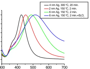
Table 1. Average diameters of silver nanoislands for different deposition conditions Mass thickness (nm) Deposition rate (Å/s) Annealing temperature (ºC) Annealing time (min) Average diameter (nm) 20 0.14 - - 80 20 0.14 300 10 120 6 0.06 150 1 30 2 0.03 150 2 40 Figure 2 compares the optical absorption spectra of silver island films prepared using different mass thicknesses, annealing temperatures, and durations, with one of the films further covered with a 10 nm thick silicon oxide layer. These results agree well with our finite-difference time-domain simulations and the SEM images displayed in Fig. 1. Larger mass thicknesses lead to red-shifted plasmon resonance because of the formation of larger nanoislands and sharper plasmon resonance is observed for the metal film annealed at a higher temperature and/or for a longer time. Also, the presence of silicon oxide layer red-shifts the resonance because of its refractive index (which is larger than that of air), as also shown in [18]. This comparison proves that the plasmon resonance wavelength of these silver nanoisland films can be conveniently tuned in a broad spectral range by changing the deposition parameters. Our experiments have also shown that this technique is reproducible and we have very good control over the resonance conditions of these silver nanoisland films through the aforementioned parameters.
300 400 500 600 700 0.0 0.2 0.4 0.6 0.8 1.0 A b so rbanc e (a.u .) wavelength (nm) 4 nm Ag, 300 0C, 20 min. 2 nm Ag, 150 0C, 2 min. 6 nm Ag, 150 0C, 2 min. 6 nm Ag, 150 0C, 2 min.+Si xOy
Fig. 2. Optical absorption spectra of silver with film thickness of 4 nm annealed at 300ºC for 20 min, silver (2 nm) annealed at 150 ºC for 2 min, silver (6 nm) annealed at 150ºC for 2 min, and silver (6 nm) annealed at 150 ºC for 2 min and subsequently also covered with a 10 nm thick SixOy layer.
3. Experimental characterization and theoretical analysis of localized plasmon-coupled nanocrystal emitters
Metal-enhanced luminescence is based on the interactions between the emission of the luminescent material and surface plasmons (or localized plasmons); in general, there are three basic mechanisms that influence the luminescence of materials close to metal films, metal structures, or metal particles [6-12, 17]: 1.) Highly localized electric field in the near-field of the metal particles, which causes luminescence enhancement if the excitation wavelength is close to the plasmon resonance wavelength, 2.) Increased radiative recombination rate of the luminescent material (as a result of the Förster-type energy transfer leading to radiative decay), which causes luminescence enhancement if the emission wavelength is close to the plasmon resonance wavelength, and 3.) Increased nonradiative recombination rate, which causes luminescence quenching.
The first two mechanisms (the field localization and the increase in radiative recombination rate) enhance the luminescence, while the last competing mechanism (the increase in nonradiative recombination rate) quenches it. Such luminescence quenching via increased nonradiative recombination rate is caused by resonant energy transfer leading to nonradiative decay (nonradiative energy transfer) [19]. The spacing between the plasmonic structure and the luminescent material and also the size of the metal nanoparticles affect the balance between the quenching and enhancement mechanisms. For smaller metal particles, absorption is more dominant in the total extinction, and the optical absorption by metal nanoparticles is responsible for quenching. Therefore, the size of metal nanoparticles should be large enough to suppress quenching (for example, >20 nm for silver). As a result, a careful design has to be made to minimize the influence of quenching and maximize effects of the enhancement interactions. To demonstrate the localized plasmon coupling of luminescent nanocrystals in the proximity of metallic nanostructures, we form closely-packed CdSe/ZnS nanocrystal films and Ag nanoisland films separated by very thin silicon oxide layers (thin dielectric spacers). To compare the effect of localized plasmons on the spontaneous emission characteristics of these nanocrystals, we also prepare two sets of control groups: one set with the same nanocrystals directly placed on the identical Ag nanoisland films (with no spacer), and the other set only with the same nanocrystals alone (with no metal film or no spacer). To obtain relatively uniform closely-packed CdSe/ZnS films, we drop-cast high-concentration nanocrystal solution (e.g., in chloroform) in multiple microdroplets of controlled volume covering the entire chip surface and evaporate the solvent of the nanocrystal solution on the chip in a chamber with controlled uniform vapor pressure. These nanocrystals were synthesized at Evident Technologies and they were also used and described in our previous work of fabricating white NC-LEDs [3, 20-22] and ultraviolet NC-scintillators [23]. Furthermore, using plasma-enhanced chemical vapor deposition (PECVD), we lay down silicon oxide layers at reduced deposition rates to control their film thickness well. In PECVD, we deposit SixOy spacer with an optimal thickness of 10 nm to provide the critical
spacing to safely avoid quenching. Placing such a spacer of right thickness between the nanocrystal emitters and the plasmonic nanoparticles is one of the critical factors, which spatially determines the level of plasmonic interaction.
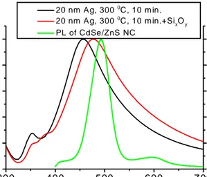
We further carefully tune the plasmonic resonance of the nanosilver film to match the emission spectrum of the nanocrystals. This is another critical factor that spectrally determines the level of plasmon coupling. For a proof-of-concept demonstration, we use CdSe/ZnS nanocrystal emitters of 1.9 nm in diameter with a size distribution of ± 5 % and a corresponding peak emission wavelength of 492 nm. For this luminescent material, we use Ag nanoislands that are optimized by depositing a mass thickness of 20 nm at a rate of 0.1 Å/sec and annealing at 300 ºC for 10 minutes under nitrogen purge. These deposition and annealing conditions lead to a silver island diameter of >20 nm (see Fig. 1 and Table 1), avoiding possible quenching that would otherwise arise from the formation of too small metal islands (with diameters <20 nm). Figure 3 displays the optical absorption spectra of the prepared silver island films with and without a 10 nm thick silicon oxide spacer on the top, with the
former exhibiting an excellent spectral overlap with the PL spectrum of CdSe/ZnS nanocrystals in film. Here compared to the peak emission wavelength of the nanocrystals, the plasmonic resonance of the metal island film coated with the silicon oxide film is intentionally obtained at a slightly shorter wavelength (with an empirically optimized blue shift of 17 nm) to compensate for the red shift of the plasmonic resonance and to spectrally match better when the nanocrystal film is actually in the proximity of the metal film (effectively increasing the dielectric constant of the medium).
300 400 500 600 700 0.0 0.2 0.4 0.6 0.8 1.0 0.0 0.2 0.4 0.6 0.8 1.0 N o rm al iz e d pho to lu m ine sce nc e No rm a liz ed ab so rba n c e wavelength (nm ) 20 nm Ag, 300 0C, 10 m in. 20 nm Ag, 300 0C, 10 m in.+Si xOy PL of CdSe/ZnS NC
Fig. 3. Optical absorption spectra of nano-silver film (with a mass thickness of 20 nm and annealed at 300 ºC for 10 min) and that also covered with a 10 nm thick SixOy layer, compared
with the photoluminescence spectrum of CdSe/ZnS nanocrystals (of 1.9 nm in diameter).
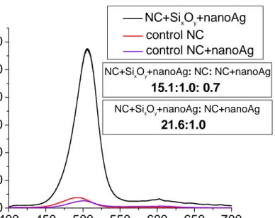
Figure 4 shows collective photoluminescence spectrum from the CdSe/ZnS nanocrystal emitters on the top that are closely packed in the proximity of nano-silver film on the bottom, separated by a SixOy spacer film between them, when excited at 325 nm with He-Cd laser of
our photoluminescence setup at room temperature, along with those of the control groups. In these PL spectra, despite the random distribution of the closely-packed nanocrystals and silver nanoislands, we observe significant enhancement (of 21.6 times) in the ensemble photoluminescence average of the CdSe/ZnS nanocrystals + SixOy + nanoAg sample with
respect to the control group of the same CdSe/ZnS nanocrystals with identical nanoAg but no SixOy spacer. In all of these characterizations, note again that the same nanocrystals of equal
amount are used and all PL measurements are taken under identical conditions.
This significant enhancement of photoluminescence is the first observation of localized plasmon coupling with CdSe/ZnS core-shell nanocrystal emitters using such randomly-distributed metallic nanoislands. In these PL experiments, optically exciting these nanocrystals at a wavelength far away from the plasmonic resonance, the effect of localized electric field observed in the vicinity of metallic nanoislands (only if excited around the plasmon resonance wavelength) makes no contribution to the PL enhancement of the nanocrystal emitters here. Therefore, this large contrast observed in the respective PL intensities stems from the interplay of only the remaining two affects: a) the radiative energy transfer making spontaneous emission from the nanocrystals stronger, which is dominant in the case of the strongly enhanced sample CdSe/ZnS nanocrystals + SixOy + nanoAg when
there is a SixOy spacer of right thickness (thick enough to prevent nonradiative decay and thin
enough to see the increased photon density of states in the proximity of the plasmonic structures, as also discussed in [24]), and b) the nonradiative energy transfer making the
spontaneous emission from the nanocrystals weaker, which is dominant in the case of the strongly quenched control group CdSe/ZnS nanocrystals + nanoAg when the nanocrystals are directly on top of the metal. We observe that quenching is dominant only for distances less than about 5 nm between the metallic structures and the nanocrystal emitters because resonant energy transfer decays very rapidly with the distance away from the surface of the metal nanoparticles. When compared to the other control group of the same nanocrystals without Ag nanoislands (when there is no plasmon coupling), the PL enhancement factor is found to be 15.1-fold, which implies that laying the nanocrystals directly on the Ag nanoislands without a spacer is quenching the luminescence by ~ 70% (15.1/21.6) compared to the luminescence of the nanocrystals on their own. On the other hand, the effect of increased recombination rate is found to decay away over distance slower, and thus it is influential in longer distances (up to about 25 nm from the surface of the metal nanoparticles [13]). As a result of this distance dependent behavior, such localized plasmon enhanced luminescence is possible only for spacing of about 5-25 nm (if only radiative energy transfer at the luminescence wavelength is to be utilized). To avoid quenching and make use of the enhancement mechanisms (before decaying away over the distance), a spacing of about 10 nm is experimentally found to be optimal.
400
450
500
550
600
650
700
0
5000
10000
15000
20000
25000
30000
NC+SixOy+nanoAg: NC+nanoAg
21.6:1.0
Pho
tolu
m
ine
s
c
enc
e (
c
ount
s
)
wavelength (nm)
NC+Si
xO
y+nanoAg
control NC
control NC+nanoAg
NC+SixOy+nanoAg: NC: NC+nanoAg
15.1:1.0: 0.7
Fig. 4. Photoluminescence peak intensity of CdSe/ZnS nanocrystals with nano-silver (20 nm) and a dielectric spacer (10 nm silicon oxide) between them is 21.6 times stronger than that of the same CdSe/ZnS nanocrystals with identical nano-silver (20 nm) but no dielectric spacer and is 15.1 times stronger than that of the same CdSe/ZnS nanocrystals alone.
For the comparison of (NC+SixOy+nanoAg) : NC : (NC+nanoAg), the photoluminescence enhancement ratio is measured to be 15.1 : 1.0 : 0.7. Integrating the area under the PL curves of the nanocrystal emitters with and without plasmonic resonance over the entire emission wavelength range, we also find that the total number of photons emitted from the nanocrystals in the case of localized plasmon coupling is 12 times larger than the case of no plasmon coupling. Here such a large PL enhancement is experimentally achieved because of careful spectral tuning of the plasmon resonance to overlap with the nanocrystal emission and careful spatial placement of plasmonic nanostructures with respective to the nanocrystal emitters (separated by a dielectric spacer). As a result, very high enhancement factors are possible with
such randomly-distributed silver nanoislands. Even larger enhancement factors may be obtained if the plasmonic resonance wavelength is also close to the excitation wavelength because this further localizes the incident field in the close vicinity of the metal nanostructures so that the nanocrystals are optically pumped effectively very strongly.
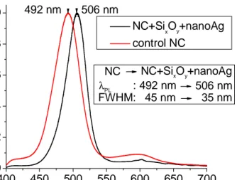
In addition to the luminescence enhancement, the resulting PL peak wavelength of the nanocrystal emitters is shifted from 492 nm to 506 nm (by 14 nm) when coupled with localized plasmons as shown in Fig. 5. We observe this emission shift not only in the enhanced nanocrystal emitters, but also in the quenched ones because both of them are influenced by localized plasmons, as also displayed in Fig. 4. Depending on the resonance frequency of the coupled plasmon, we observe that it is possible to red-shift the peak emission wavelength. Additionally, we report that the photoluminescence FWHM of these nanocrystal emitters is reduced from 45 nm to 35 nm (narrowed down by 10 nm corresponding to more than 22% reduction) as a result of the interaction with the nanometallic film. Figure 5 emphasizes these changes by comparing the normalized photoluminescence graphs of the sample CdSe/ZnS nanocrystals + SixOy + silver island film and the control group of the same
nanocrystals alone. This is the first report of modified spontaneous emission from plasmon-coupled nanocrystal emitters including the emission linewidth and peak modifications via localized plasmon coupling.
400 450 500 550 600 650 700 0.0 0.2 0.4 0.6 0.8 1.0 506 nm N o rm al iz ed phot ol um ines cen c e wavelength (nm) NC+SixOy+nanoAg control NC 492 nm 506 nm NC NC+SixOy+nanoAg λPL : 492 nm FWHM: 45 nm 35 nm
Fig. 5. Photoluminescence peak wavelength of CdSe/ZnS nanocrystals is shifted by 14 nm (from 492 nm to 506 nm) and its emission linewidth is reduced by 10 nm (from 45 nm to 35 nm) with localized plasmon coupling.
In Fig. 5, the red-shift of the nanocrystal emission is attributed to the interactions between the permanent dipole moment related to the asymmetry of the CdSe/ZnS nanocrystals and the dipole moment induced in the silver nanoislands. On the other hand, though experimentally verified, the theoretical understanding of the physical conditions and the associated processes for the linewidth reduction is not completely clear. The increased radiative recombination rate requires homogenous broadening of emission; this is also evidenced by the increased total number of emitted photons (i.e., the increased area under the PL spectrum) in the case of plasmon coupling. But for the closely-packed nanocrystals with high degree of disorder in film, there are also equally strong dipole-dipole interactions between the nanocrystals themselves and inhomogeneous broadening mechanisms in effect, which makes the interplay between such intra-particle distance-dependent interactions complicated. Due to the spectral optimization of plasmonic nanostructures to the peak wavelength of the collective emission
from the nanocrystals in our samples, one possible explanation is based on the better plasmon coupling of those nanocrystals in the ensemble only with the size close to the average diameter, which contribute to the collective emission only around the peak emission wavelength. Further theoretical and experimental study is currently in progress to understand the complex nature of these interactions.
4. Conclusion
As a proof-of-concept demonstration, we showed that the localized plasmons of metal nanoisland films provide the ability to significantly modify and control the collective spontaneous emission of nanocrystals in their proximity (including emission linewidth and peak emission wavelength in addition to emission intensity). Using randomly-distributed Ag nanoparticles, we demonstrated plasmonic resonance carefully tuned spectrally and carefully optimized spatially to couple well with the proximal CdSe/ZnS core-shell nanocrystal emitters. By doing so, for the first time to the best of our knowledge, we achieved to significantly reduce the emission linewidth (by 10 nm corresponding to 22% reduction of FWHM) and to significantly shift the photoluminescence peak wavelength (by 14 nm), while also significantly enhancing collective spontaneous emission intensity by 15.1 and 21.6 times compared to the control groups of the same nanocrystals alone (when there is no plasmon coupling) and those with identical nano-silver but no dielectric spacer (when the nanocrystal emission is quenched), respectively.
To obtain such localized plasmonic nanostructures, we used metal island film formation, which provides the advantages of easy implementation, reproducibility, and tunability. By changing the mass thickness, evaporation rate, annealing temperature, and annealing time in this method, we conveniently spectrally optimized the resonance wavelength of the silver island film to match the emission spectrum of the nanocrystals. We also investigated the distance dependence of the plasmonic interactions on the photoluminescence of semiconductor nanocrystals and observed strong quenching (70%) when the nanocrystal emitters were closely packed directly on top of the silver island film (with no spacer in between them). Therefore, in addition to spectral tuning of the plasmonic resonance to overlap with the nanocrystal emission, the spacing between the plasmonic structure and the nanocrystal emitters must be optimized considering the spatial behaviors of radiative vs. nonradiative energy transfer between the metal and the semiconductor nanocrystals.
In conclusion, we demonstrated the utilization of metallic nanoisland films (made of silver) to plasmon-engineer spontaneous emission from the core-shell nanocrystals (made of CdSe/Zn) including the important emission features such as emission linewidth and peak, in addition to emission intensity. Using such randomly-distributed metal nanoparticles, high enhancement factors of plasmon-coupled photoemission were achieved thanks to careful spectral and spatial tuning, when compared to the previous literature of metallic island formation and metallic colloidal approaches.
Acknowledgments
This work is supported by EU-PHOREMOST Network of Excellence 511616 and Marie Curie European Reintegration Grant MOON 021391 within the 6th European Community Framework Program and TUBITAK under the Project No. 107E088, 106E020, 104E114, 105E065, and 105E066. Also, HVD acknowledges additional support from the Turkish Academy of Sciences Distinguished Young Scientist Award (TUBA GEBIP) and European Science Foundation (ESF) and European Heads of Research Councils (EuroHORCS) European Young Investigator Award (EURYI) Programs. IMS and SN acknowledge TUBITAK Graduate Fellowship Program. The authors are also pleased to acknowledge using the facilities of Bilkent University Nanotechnology Research Center (Founder Prof. E. Ozbay) and Advanced Research Laboratories (Founder Prof. S. Ciraci). The authors would further like to thank TUBITAK MRC (Director O. Yetis and Prof. A. A. Kaya, Material Institute) for the use of high-resolution scanning electron microscope in this work.